


I. INTRODUCTION
The microstrip patch antennas are most popular in wireless and RF applications due to their vital advantages, such as low cost, lighter weight, and easy fabrication. Recently, the demand for the antenna has been increasing which can be used for more than one application that reduces the cost and number of antenna requirement of individual applications. The multiband antenna can fulfill the demand for various wireless applications, such as GSM (880 to 960 MHz), UMTS (1920 to 2170 MHz), Wi-MAX (2.5–2.69, 3.3–3.7, and 5.25–5.85 GHz), WLAN (2.4–2.484, 5.15–5.35, and 5.725–5.85 GHz), PCS (1850–1990 MHz), IMT-2000 (1920–2170 MHz), DCS (1710 1880 MHz), GPS, and CDMA [Reference Yoon, Chul Rhee and Kil Jang1, Reference Jang and Choi2]. Several multi-frequency microstrip antenna designs have been proposed by the researchers in the literature. These are employing stacked structure with shorting pin [Reference Anguera, Font, Puente, Borja and Soler3–Reference Elsadek6], using PIFA configurations [Reference Nashaat, Elsade and Ghali7–Reference Chiu and Chi9], offering a multi-frequency dielectric resonator [Reference Huitema, Koubeissi, Mouhamadou, Arnaud, Decroze and Monediere10], introducing a slot and notch of different shapes in a proper position on the radiating patch [Reference Tine, Kabalan, EI-Hajj and Rammal11–Reference Dasa, Sarkarb and Chowdhuryc15], applying slotted ground structures [Reference Elsheakh and Abdallah16, Reference Liu, Wu and Dai17] and using folded patch structures [Reference Chiu, Chang and Chi18, Reference Chi and Wong19]. On the other hand PIN diodes, switches, varactor diodes, and chip capacitors are used for multiband operations [Reference Kehn, Ng, Quevedo-Teruel and Rajo-Iglesias20].
In the above proposed structures, they have only described two or three resonating frequencies with having some limitations, such as cross-sectional area, complexities in designing, variable gain and efficiency, and creating impedance matching problem.
These limitations can be minimized by modifying the feed structure in the form of L–strip. This feeding has interesting features, such as simplicity in structure and ease in fabrication that reduce the impedance matching problem. This arises in probe feeding because L-strip feeding creates a capacitance which minimizes the inductance of the vertical portion responsible for good impedance matching characteristics. Due to these attractive features of the L-strip, the novel multiband S-shaped patch antennas with L-strip feeding are proposed. The objective of presentation of the paper is providing the multiband characteristics by loading a notch on both sides of the radiating patch, so that for exciting the patch is used the L-strip feeding. The antenna characteristics are also observed for the different substrate materials, so the simulated results are verified with the experimental results. Optimization of dimensions and detail description of the antennas are discussed in the following sections.
II. ANTENNAS LAYOUTS AND THEIR CONSTRUCTION PROCEDURES
In this paper the L-strip form feeding is used to design the structures. The proposed antenna structures with L-strip feeding have been described the several resonating frequencies with having some advantages of no cross-sectional area, simplicity in designing and construction, stable gains and efficiencies, and creating the impedance matching. Due to these attractive features of the L-strip, the interesting multiband S-shaped patch antennas with L-strip feeding are proposed.
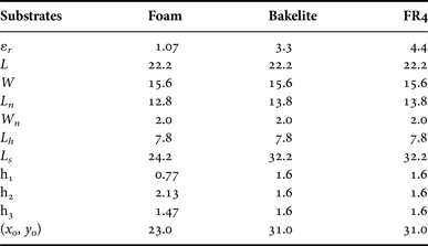
The proposed antennas are constructed on the different substrate materials, such as Foam, Bakelite and FR4 with relative permittivity of ε r = 1.07, 3.3, and 4.4, respectively, which are shown in Fig. 1. All three antenna structures are similar in shape but have different characteristics. The constructed antennas on FR4 and Bakelite substrates are not able to produce the frequency above 20 GHz but the similar radiating structure, which is fabricated on foam substrate, has produced the multiband performances from 6 to 45 GHz. The proposed antenna structures are simulated, tooled, fabricated, and measured in order to obtain the multiband characteristics.

Fig. 1. Photographs of the simulated and fabricated antennas.
The suitable optimization of the design parameters, such as length and width of the patch, allocation of the notch on the patch, dimensions of the L-strip, position of the feed point and the horizontal part of the L-strip inside the patch have influenced the multiband characteristics. The parametric studies of the loaded slot in patch (W and L) and feed position (x 0, y 0) accompanying other structural parameters of the antennas are given in Table 1.
Table 1. Parametric studies of the S-shaped antennas with L-strip feeding, which are constructed on three different substrates (all dimensions are in mm).

Figure 2 shows the current distribution of the proposed Ant.1 at different resonating frequencies. From the figure, it is observed that when two notches incorporate on the patch, it alters the resonance behavior of the initial patch and by the proper selection of dimensions and positions of the L-strips the current directions and its strengths on the patch are changed. Hence, the proper positions of the notch and L-strips strongly affect the antenna to achieve the multiband characteristics.

Fig. 2. Simulated current distributions of the proposed Ant.1 at different resonating frequencies.
III. CIRCUIT MODAL AND ANALYSIS OF THE PROPOSED ANTENNAS
A) Analysis of the notch loaded on the rectangular patch
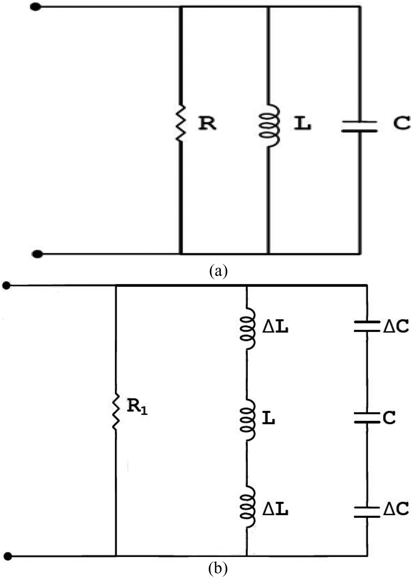
The simple rectangular patch antenna is modeled as a parallel RLC circuit, as shown in Fig. 3(a). The circuit parameters RLC are calculated using cavity model.

Fig. 3. (a) Equivalent circuit of the rectangular patch. (b) Equivalent circuit of the notch-loaded patch.
The notch loaded on the patch leads to the additional series notch inductance ΔL and gap capacitance ΔC in series with L and C as shown in Fig. 3(b). That modifies the equivalent circuit of the rectangular patch antenna. The series inductance (ΔL) and gap capacitance (ΔC) can be calculated as
 $$\Delta L=\displaystyle{{h\mu _0 \pi } \over 8}\left({\displaystyle{{L_n } \over L}} \right)\comma \;$$
 $$\Delta C=\left({\displaystyle{{L_n } \over L}} \right)C_g\comma \;$$
where, μ 0 = 4π × 10−7 H/m, and L n , C g , and R 1 are the depth of the notch, the gap capacitance, and the resistance after cutting the notches, respectively. The total inductance L 1 and capacitance C 1 are defined as
 $$L_ 1=L+ 2\Delta L\comma \;$$
 $$C_1=\displaystyle{{C\Delta C} \over {2C+\Delta C}}.$$
Two resonant circuits coupled through coupling capacitance (C c ) are shown in Fig. 4, so that one is the initial RLC of the rectangular patch and another is after cutting the notches.

Fig. 4. Equivalent circuit of the notch-loaded rectangular patch antenna.
B) Analysis of the L-strip feeding
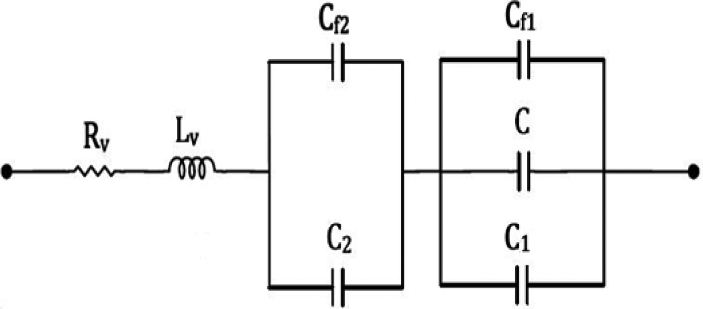
Figure 5 shows the equivalent circuit of the L-strip feed. The vertical part of L-strip is equivalent to a series of combination of resistance (R V ) and inductance (L V ), which can be calculated as,

Fig. 5. Equivalent circuit of the L-strip feeding.
 $$L_v=0.2h_2 \lsqb {\rm ln}\lcub 2h/\lpar w_s+t_s \rpar \rcub +0.2235\lcub \lpar w_s+t_s \rpar /h_2 \rcub +0.5\rsqb \comma \;$$
and
 $$R_v=4.13 \times 10^{ - 3} h_2 \sqrt {f\rho /\rho _{cu} } /\lpar w_s+t_s \rpar \comma \;$$
where, w s and t s are the width and thickness of the L-strip, h 2 is the height of the vertical portion of the L-strip, ρ and ρ CU are the specific resistance of the strip and specific resistance of copper, i.e. 1.72 × 10⁻⁶ cm.
The total height of the substrate is divided into three parts h 1, h 2, and h 3, which introduces the capacitances C 1 and C 2. C 1 is the capacitance between patch and horizontal part of the L-strip whereas C 2 is the capacitance between horizontal part and ground.
 $$C_1=\displaystyle{{\varepsilon _r \varepsilon _0\, L_h w_s } \over {h_3 }}\comma \;$$
 $$C_2=\displaystyle{{\varepsilon _r \varepsilon _0 w_s L_h } \over {h_1+h_2 }}\comma \;$$
where, L h is the horizontal length of the L-strip, h 1 is the height between ground plane and microstrip line, h 2 is the height of the vertical portion of the L-strip, h 3 is the height between horizontal part of L-strip and radiating patch, ε r is the relative permittivity of the material, and ε 0 is the permittivity of the free space.
The open end of the L-strip will generate the fringing fields, which increase the length of the L-strip slightly. This corresponds to extra capacitance (C f ) given as,
 $$c_f=l_e \lpar \varepsilon _e \rpar ^{ - 1/2} /cZ_0\comma \;$$
in which, l e and Z 0 are the effective length and characteristic impedance of the L-strip, respectively, where,
 $$l_e=\displaystyle{{0.412\lpar \varepsilon _e+0.3\rpar \lpar w_s /h+0.264\rpar } \over {\lpar \varepsilon _e - 0.258\rpar \lpar w_s /h+0.8\rpar }}.$$
Equation (9) can be used to calculate the fringing capacitance (C f1) and (C f2).
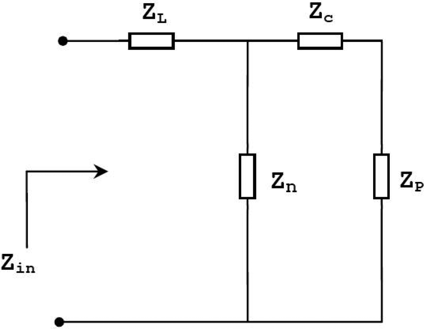
Using the equivalent circuit model, the input impedance of the proposed antennas with L-strip feeding is easily analyzed with the circuit as shown in Fig. 6.

Fig. 6. Equivalent circuit of the proposed antennas with L-strip feeding.
The resultant input impedance (Z in ) of the antenna seen from the terminals is given by
 $$Z_{in}=Z_L+\displaystyle{{Z_n \lpar Z_C+Z_P \rpar } \over {Z_n+Z_P+Z_P }}.$$
Now using equation (11), different parameters of the antennas such as reflection coefficient, VSWR, and Return loss are calculated.
IV. DETAILED INFORMATION AND DISCUSSIONS
The frequency versus the return loss curves for the optimum designs are shown in Figs. 7, 8, and 9. The performances of these three antenna structures are investigated and their characteristics are compared. From the figures, it is noted that the operating characteristics of the Ant.1 is better than Ant.2 and Ant.3 in respect of operating frequency bands. The detailed information about the designed antennas is discussed in this section. The simulation processes of the proposed antennas are performed by method of moment based on the simulator known as IE3D and their measurement procedures are accomplished by a spectrum analyzer.

Fig. 7. Plot of the return losses versus frequency for the Ant.1.

Fig. 8. Plot of the return losses versus frequency for the Ant.2.

Fig. 9. Plot of the return losses versus frequency for the Ant.3.
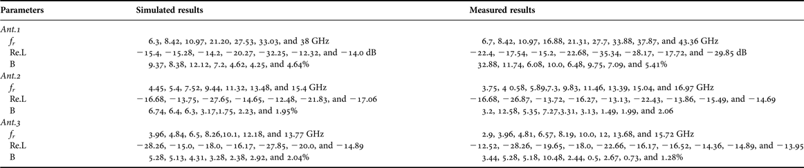
The return losses versus frequency of the Ant.1 constructed on the foam substrate are shown in Fig. 7. In this figure the simulated and measured results are plotted together stating that they are in good agreement. It is observed from the figure that Ant.1 is resonating at different operating frequencies in between 6 to 45 GHz. So that, the simulated resonating frequencies are noticed at 6.30, 8.42, 10.97, 21.20, 27.53, 33.03, and 38 GHz with corresponding bandwidth of 9.37% (6.1–6.7 GHz), 8.38% (8.0–8.7 GHz), 12.12% (10.39–11.73 GHz), 7.2% (20.44–21.97 GHz), 4.62% (26.88–28.15 GHz), 4.25% (32.66–33.26 GHz), and 4.64% (37.07–38.83 GHz) and the return losses obtained at these frequencies are −15.4, −15.28, −14.2, −20.27, −32.25, −12.32, and −14.0 dB, respectively. Also, the measured results demonstrate that the antenna resonates at 6.7, 8.42, 10.97, 16.88, 21.31, 27.7, 33.38, 37.87, and 43.36 GHz with corresponding bandwidth of 32.88% (6.1–8.5 GHz), 11.74% (10.42–11.72 GHz), 6.08% (16.1–17.11 GHz), 10.0% (20.72–22.9 GHz), 6.48% (26.88–28.68 GHz), 9.75% (32.48–35.81 GHz), 7.09% (36.35–39.02 GHz), and 5.41% (42.07–44.41 GHz) and return losses obtained at these frequencies are −22.4, −17.54, −15.2, −22.68, −35.34, −28.17, −17.72, and −29.85, respectively. The simulated results are in close agreement with the measured results.
Figure 8 shows the simulated and measured return losses versus frequency of the Ant.2. The Ant.2 is fabricated on the Bakelite substrate and provides the multiband characteristics from 3 to 20 GHz. The antenna is resonating at 4.45, 5.4, 7.52, 9.44, 11.32, 13.48, and 15.4 GHz with corresponding bandwidth of 6.74% (4.3–4.6 GHz), 6.4% (5.3–5.65 GHz), 6.3% (7.23–7.7 GHz), 3.17% (9.3–9.6 GHz), 1.75% (11.3–11.5 GHz), 2.23% (13.3–13.6 GHz), and 1.95% (15.2–15.5 GHz), respectively. The measured resonating frequencies are observed at 3.75, 4.58, 5.89, 7.3, 9.83, 11.46, 13.39, 15.04, and 16.97 GHz with corresponding bandwidth of 3.2% (3.69–3.81 GHz), 12.58% (4.2–4.76 GHz), 5.35% (5.64–5.95 GHz), 7.27% (7.03–7.56 GHz), 3.31% (9.5–9.82 GHz), 3.13% (11.29–11.65 GHz), 1.49% (13.3–13.5 GHz), 1.99% (14.9–15.2 GHz), and 2.06% (16.8–17.15 GHz).
The simulated and measured return losses of the Ant.3 versus frequency are demonstrated in Fig. 9. The Ant.3 is fabricated on FR4 substrate and is resonating at different frequencies from 2 to 16 GHz. The simulated results are verified with the measured results and it is found that practically slight variations are occurred between them. It is noticed from the figure that the simulated resonating frequencies are observed at 3.96, 4.84, 6.5, 8.26, 10.1, 12.18, and 13.77 GHz, whereas the measured resonating frequencies are occurred at 2.9, 3.96, 4.81, 6.57, 8.19, 10.0, 12.0, 13.68, and 15.72 GHz. Hence, the bandwidths associated with these frequencies are 5.28, 5.13, 4.31, 3.28, 2.38, 2.92, and 2.04% in simulation and 3.44, 5.28, 5.18, 10.48, 2.44, 0.5, 2.67, 0.73, and 1.28% in measurement, respectively.
The operating characteristics of the proposed antennas are summarized in Table 2.
Table 2. Operating characteristics of the proposed antenna structures. It should be noted that, f r , Re.L, and B are the abbreviations of the resonating frequencies, return losses, and bandwidths, respectively.

Figure 10 shows the measured gain versus frequency and the measured efficiency versus frequency of the proposed Ant.1. It is seen from the Fig. 10 that, the proposed design gives the negative gains in the frequency range of 0–6 GHz because at these frequencies, antenna does not resonate, while at the operating frequencies above 6 GHz, the antenna provides the positive gains of 8.55, 9.74, 10, 9.68, 10, 6.75, 7.2, 8.03, 6.6, 6.38, and 6.5 dBi. The variation of the efficiency with respect to frequency graph is also plotted in Fig. 10. The maximum and minimum values of the measured efficiencies of the antenna are 93 and 30%, respectively, with respect to corresponding resonating frequency bands.

Fig. 10. Curves of the measured gain with frequency and the measured efficiency with frequency for Ant.1.
The measured E and H-planes radiation patterns of the proposed Ant.1 at different resonating frequencies of 6.3, 8.42, 10.97, 16.0, 21.2, 27.53, 33.03, 38.0, and 45 GHz are plotted in Fig. 11(a)–(i). Here, the antenna radiates most of its energy in the direction of maximum radiation. The number of lobes in the pattern represents a division of the radiated energy and the nulls represent angles at which no energy is transmitted.

Fig. 11. Measured E- and H-plane radiation patterns at the different resonating frequencies of the Ant.1.
According to the obtained results, the proposed designs with multi-band frequency performances can be potentially helpful to use in the recent wireless telecommunication systems needful of multiple applications.
It is also noteworthy that, the picture of the laboratory at which the proposed microstrip notch-loaded rectangular S-shaped patch antennas using L-strip feeding were tooled, constructed, and tested is shown in Fig. 12.

Fig. 12. Photo of the antenna lab.
V. CONCLUSION
Three L-strip fed notch-loaded microstrip patch antennas, which were modeled, tooled, and constructed on the three substrates such as Foam, Bakelite and FR4, have been studied for multiband applications. The designed antennas have been simulated and the results are verified experimentally. Furthermore, they show the good radiation characteristics, high gains, and efficiencies at different resonating frequencies that can be used for different applications in the multi-band frequencies from 6 to 45 GHz, 3 to 20 GHz, and 2 to 16 GHz. As well as their characteristics, they can be pointed for low cost, lighter weight, and easy fabrication, so that they can be used for more than one application that reduces the cost and number of antenna requirement of individual applications.
 Mohammad Alibakhshi-kenari was born in 24 February 1988 in Iran, Mazandaran, Fereidounkenar. He received the B.S. and M.S. degrees in the Electrical Engineering, field of Telecommunication from the Islamic Azad University, Najafabad Branch of Esfahan, Iran on February 2010 and the Islamic Republic of Iran, Shahid Bahonar university of Kerman on February 2013, respectively. His main areas of interest in research are microwave and millimeter wave circuits, radars, antennas and waves propagation, composite right/left-handed transmission lines (CRLH-TLs), metamaterial (MTM) applications, integrated RF technologies, embedded systems, electromagnetic waves applications and wireless telecommunication systems.
He is now ”Editor-in-Chief” in Journal Club for Electronic and Communication Engineering (JCECE) and also works as a reviewer in the several ISI journals such as Elsevier, Taylor & Francis, Wiley, ACES and etc. M.A-kenari has served as a Member of the Technical Program Committee (M-TPC) of some of the international conferences such as APACE 2014, APPEIC 2014, MobiWIS 2014, ICEPIT 2014, CICN 2014, ADVCIT 2014, DPNoC 2015, MobiApps 2015 and etc. So far, he has been published several papers. Also, the Master Thesis of M.A-kenari entitled “Designing and Fabricating the Ultra Compact and UWB Antennas based on Metamaterial Transmission Lines with Application in Wireless Radio Transceivers” was approved and granted by Iran Telecommunication Research Center (ITRC) on December 2012 with grant number of 6987/500/T.


Target article
Retraction Notice
Related commentaries (6)
A new compact UWB traveling-wave antenna based on CRLH-TLs for embedded electronic systems
Designing an ultra-wideband electromagnetic waves receiver with new architecture for RF and wireless applications
Introducing the new wideband small plate antennas with engraved voids to form new geometries based on CRLH MTM-TLs for wireless applications
Miniaturized printed monopole antenna with applying the modified conductor-backed plane and three embedded strips based on CPW for multi-band telecommunication devices
Modeling and constructing the microstrip notch-loaded rectangular S-shaped patch antennas using L-strip feeding for multi-band frequency performances in the recent wireless telecommunication systems
Significant measureable development of inductance gain per unit of space in loop fractals