


I. INTRODUCTION
The aim of this paper is to investigate the fractal geometrical strategy in order to achieving an appreciable inductive increase given two important restrictions: that it occupies the same design space and, more significantly, that it requires only a single fabrication layer. The pursuit of miniaturization and simplification of monolithic circuitry, for integrated implementation in printed circuits, and radio frequency identification (RFID) for example, urges the need for renewed interest in single layer planar geometries for passive components. The body of article presented addresses this urge by introducing and examining single layer planar inductors and presents a thorough investigation on metrics that are relevant to printable electronics. In addition to obvious metrics such as the raw inductance and resistance values, we have characterized the inductors in terms of its sheet properties: its sheet resistance and, the inductance per sheet/square of the components, which is meant to measure how much inductance is available for each square of resistance.
While the spiral inductor is ubiquitously utilized for a multitude of applications, it nonetheless requires at least two layers or an air bridge if it is to be used in a network in a useful manner [Reference Burghartz, Edelstein, Jahnes and Uzoh1], limiting its use for low-cost, printable circuits. Previously examined alternative single layer planar geometries include the common “loop” and the “meander.” Past studies in the meander structure [Reference Kawabe, Koyama and Shirae2] has shown that the combination of adjacent electrodes and anti-parallel current pathway leads to an early resonance because of an overwhelming capacitive coupling. The loop inductor, on the other hand, does not exhibit this disadvantage as apparently [Reference Bahl3].
Nevertheless, as in most inductors, the major drawback is the surface area, arising mainly due to the planar structure's poor ability to couple magnetically for better inductive performance. For this reason, we have implemented a simple geometrical strategy through fractalization to increase this parameter. In [Reference Stojanović, Radovanović and Radonić4] is investigated numerous fractal inductors for transformer applications such as the Hilbert and Koch fractal which proved effective. Fractals also show promise for novel antennas layouts [Reference Werner and Ganguly5], and even used as a design technique for metamaterials (MTMs) [Reference Xu, Wang and Liang6].
In this paper, we have examined the fractal derivations of the original loop due to its space filling properties [Reference Best and Morrow7]; and, although the effective electrode length increases, overall, the arrangement still essentially occupies the same space.
All structures studied are compared against each other in an all-inclusive inductance versus resistance or “L and R” gain plot. The aim of this consolidation is to demonstrate which strategies are worth pursuing for further investigations. We have achieved this by introducing an “Inductance gain” figure of merit (IG-FOM). Because higher order fractals results in a lengthened conductive pathway, both self-inductance and mutual inductance are enhanced since the fringes of the interacting magnetic field are able to couple with neighboring electrodes [Reference Robin and Souillard8]. Consequently, it is crucial that the signal's magnetic component is able to interact with the idiosyncrasy of the geometry.
To extract the parameters of interest, a Keithley capacitance-voltage unit (CVU) was used to measure the real and reactive component of the structure. The technique adopts a four-point probe system, where the current and the voltage are measured separately, with a built-in phase locked loop that identifies the phase angle difference [Reference Stauffer9].
II. FABRICATION AND CONSTRUCTION
All structures were fabricated and tested on a borofloat glass substrate with dielectric constant loss tangent of 0.004. A chrome layer of 30 nm for adhesion, followed by a 180 nm gold layer were sputtered and then etched accordingly. Figures 1(a)–1(f) show the realized inductors. The 3O 1st order candidate was constructed from the basic loop structure by rescaling it to half its size, then placing the respective number of copies in a manner that resembles the original shape. Due to the curvature of the 0th order loop, some “overshooting” at the connection points result if left unaltered; these are subsequently removed to avoid any possible fringing capacitance. A similar procedure was used for the other candidates. To arrive at the 2nd order, the 3O structure was resized appropriately then the copies laid out in semblance to it. For the 3rd order, the increasing complexity saw more prominent overshoots at the adjoints, since they naturally linked at more acute angular points; the elimination thereof resulting in the finalized structure. The square contact pads (500 µm × 500 µm) were then added for measurements. The square pads with dimensions of 500 µm × 500 µm are selected for realizing of the minimization purpose.

Fig. 1. (a) The fabricated base inductor and dimensional definitions; the set of 1st order structures in “pseudo-series” consisting of (b) 3 bases, (c) 5 bases, (d) 7 bases, (e) the 2nd order fractal (f) the fabricated 3rd order fractal based on the 1st – 3O structure, and (g) an example of a control (ctrl) structure: shown is the 3rd order series equivalent consisting of 27 base copies placed in series.
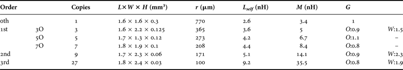
Naming conventions for fractal geometries are explicitly defined within the paper in accordance with mathematical definitions [Reference Falconer10]. A simple loop inductor was used as the base geometry from which all fractal configurations considered in this study are derived. The associated nomenclature of the fractal geometry is determined by the amount of recursion within the effective planar area of the original structure [Reference Mandelbrot, Gefen, Aharony and Peyriere11]. For instance, the “3O” fractal is equivalent to three base structures oriented in “pseudo-series” such that the overall outline resembles the base as in the previousure. These configurations are studied to determine the optimal geometry to be set as the “first-order” fractal; i.e. the first fractal derivative of the base structure. Furthermore, one of these structures is chosen for further recursion to create a 2nd order structure and once more to yield a 3rd order structure. The layouts are shown in Figs 1(a)–1(f); and, the inductance and the resistance are all compared to the base inductance L 0 and base resistance R 0. The equivalent series layouts for each fractal order were also evaluated; an example is given in Fig. 1(g) for the 3rd order.
III. EFFECT OF FRACTALIZATION
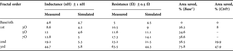
Raw inductance measurements (“Measured” column) are shown in Table 1, with a margin of error dependent on probe placement. With respect to the base or 0th order fractal, increasing both the amount of recursion (for the 1st order) and fractal order was met with a developed inductance but added resistance.
Table 1. Raw inductance, resistance, and relative conductor area-saving ratings.

Without any resistance reduction strategies, the resistance from the base to the highest order amplifies more so than the inductance: 12.6 times in resistance, and 9.9 times in inductance. These trends are revealed in Fig. 2 connected by a dashed line.

Fig. 2. Measured L and R gain plot of all structures studied comparing normalized inductance to normalized resistance. Here, the null gain line represents no tradeoffs between resistance and inductance; points that fall in the lower diagonal represents an inductance gain that is greater than resistance for a given structure. The dashed line emphasizes the L and R progression with respect to the original fractals. The inset magnifies and highlights the structures exhibiting an inductance gain; in particular, “wide” tag denotes that the electrode width was double (2H) that of the original fractal; the “paths” tag denotes the number of geometrically identical paths placed in parallel with each other.
When this trend is compared to other fractal geometries, for example the Hilbert fractal which has a meander configuration as its second-order structure, from “2nd order” to “5th order” both the inductance and effective area occupied increased five times [Reference Maric12, Reference Wang, Xu and Wang13], where for the loop base structure studied here to the 3rd order, the inductance developed 9.9 times while essentially maintaining the same occupied space.
To validate the measured results have compared the measurements to the simulated results of Agilent's ADS 2011 EM simulation tool in Table 1 under the “Simulated” column. Although the simulation does not accurately predict the inductance beyond the base structure, the measured versus simulated resistance are closely matched, with the differences being accounted by possible over etching during fabrication and under-developing during photolithography.
For example, the base inductance is measured at 4.6 nH with a resistance of 5 Ω (4.7 nH and 4.5 Ω in simulation); and we have observed a 3rd order inductance of 44.7 nH at 63.5 Ω (8.3 nH and 44.3 Ω in simulation). The appreciable accuracy of the simulated resistance values in predicting the actual values at least to the 2nd fractal order, especially in contrast to its poor predictive capabilities for the fractal structures' inductance, is further evidence that the inductive phenomenon is not simply due to the lengthening of effective conductive pathway. In particular, self-inductance does not sufficiently explain the increase. Thus we must attribute the increase to the mutual inductance that the fractal oriented loops fosters and which the simulation tool is unable to predict.
To further investigate the extent of the mutual magnetic coupling and explain the discrepancies have described the structure using known models for determining inductance contributions. If we consider just the contribution of the geometry's self-inductance to the overall inductance rating, with φ′ being the angular limits of the loop and C being the full circumference of a single loop given a radius of r, we can approximate it using the following model for circular loops [Reference Paul14]:
 $$\eqalign{L_{self} & = \displaystyle{{\mu _0 } \over {2\pi }}\vint_{\varphi ^{\prime} = 11\pi /18}^{2\pi } {\vint_{r = 0}^{r - \lpar H/2\rpar } {\displaystyle{1 \over r}} } \cr &\quad \times \left[{\vint_{\varphi = 0}^\pi {\displaystyle{{a^2 \cos \, \varphi \, \, \lpar a - {\rm rcos}\; \, \varphi \rpar } \over {\lpar a^2 + r^2 - 2\, \, {\rm arcos}\, \varphi \rpar ^{\displaystyle{3 \over 2}} }}d\varphi } } \right]rdrd\varphi {\rm ^{\prime}\comma \; }}$$
which for fractals with 1st, 2nd, and 3rd orders can be further approximated to:
 $$L_{self} = \displaystyle{{\mu _0 C} \over {2\pi }}\left\{{\ln \left({\displaystyle{{8\pi r} \over H}} \right)- \displaystyle{7 \over {18}}{\rm ln}\left({\displaystyle{{8\pi r} \over H}} \right)} \right\}.$$
For higher order fractals, since each recursion is simply scaled accordingly, we can arrive at a rough estimate by first evaluating the self-inductance of a single scaled-down loop using (2), then multiplying by the number of copies within the structure. The rough mutual inductance estimate is then [Reference Paul14]:
 $$M = L_{measure} - L_{self}.$$
As previously mentioned, the measurable increase suggests a mutual magnetic coupling which goes beyond simply the increase of the effective length as shown in Table 2. To elaborate further, a possible reason for the discrepancy between the simulated and measured inductance can be explained in terms of the mode of field that interacts with structure. Because the EM simulation tool excites the planar structure in the transverse electric mode, we can still accurately arrive at the resistance values which closely match measurements. However, to attain the true inductance of a planar inductor through interaction of fields, a transverse magnetic field is required and hence we observe the inconsistencies between simulation and measurement. Using a source meter that feeds current through the structure directly, we circumvent this problem altogether and see the true extent of mutual coupling of our fractal structures.
Table 2. Dimensional properties, self-inductance L self , mutual inductance M and IG-FOM G for the original O and doubled-width W structures.

IV. SHEET RESISTANCE AND AREA ANALYSIS
Because we have emphasized the planar aspect of the inductors examined here, especially in low cost applications which would restrict the fabrication process to a single layer, the sheet properties of the inductors are examined. For applications where conductor consumption is a concern, we also examine the conductor area taken up by each structure.
The conductor area saved was determined according to (4a) for the base (‘base’) and (4b) for the control (‘ctrl’) study. In this work, the control structure is taken as the scaled-down loop of each fractal and chaining each loop together in series (an example of a control structure for the 3rd order fractal, see Fig. 1(g)).
 $$\eqalign{&{\rm Area}\, {\rm saved}\, {\rm \lpar base\rpar =\left[{\displaystyle{{\lpar {\rm Area\; }\, {\rm of}\, {\rm base} - {\rm Area}\, {\rm of\; }\, {\rm fractal}\rpar } \over {{\rm Area}\, {\rm of}\, {\rm base}}}} \right]}\cr&\times 100 \percnt\comma}$$
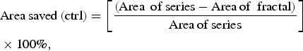 $$\eqalign{&{\rm Area}\, {\rm saved}\, {\rm \lpar ctrl\rpar =\left[{\displaystyle{{\lpar {\rm Area\; }\, {\rm of}\, {\rm series} - {\rm Area}\, {\rm of\; }\, {\rm fractal}\rpar } \over {{\rm Area}\, {\rm of}\, {\rm series}}}} \right]}\cr&\times 100 \percnt\comma}$$
We have founded that an almost 75.8% reduction was found for the highest order for the former comparison, and a 47.9% reduction for the latter. Table 1 provides the area saved for each fractal order with respect to the base (base) and equivalent series layout (ctrl). For the control layouts, however, the reduced conductor consumption for the fractal equivalent is due to the elimination of overshoots when placing the loops in a fractal layout. In general, although the inductance gain is better than the fractal equivalents, the associated resistance degradation puts this geometrical strategy at a disadvantage. These are investigated further and quantized in the sheet analysis.
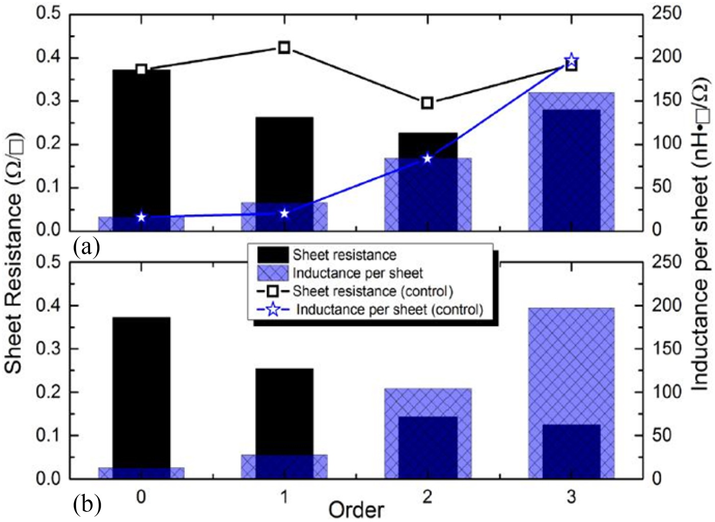
Sheet resistance analysis in Fig. 3(a) have revealed that for the first two orders, the resistance per square was lower than the basic loop inductor, up until 3rd order fractal which exhibited a slight degradation. However, when for each geometry comparing the sheet resistance to the measured inductance (inductance per square), a clear development is observed. In the same figure, the series configuration (control) was also contrasted with the equivalent series layout (Fig. 3(a)). The assessed sheet resistance was consistently higher with the series equivalents than its comparable fractal structure. In addition, the inductance per sheet resistance for the control also produced poorer ratings, with the exception of the 3rd order equivalent structure.

Fig. 3. Measured sheet resistance and inductance per square analysis for each fractal order extracted from (a) the original structures and its equivalent series layout (control); and, (b) with electrode width doubled from the original. Here, smaller black bars and larger checkered bars mean higher inductance per square area of resistance.
The effect of doubling the electrode width (from H to 2H) for all fractal orders higher than zero is also shown in Fig. 3(b). While for the 3rd order the inductance decreased by approximately half of the original amount, the resistance fell to under a quarter of the original electrode width. Furthermore, we found that doubling the electrode width had dramatically reduced the sheet resistance at higher orders.
An alternative solution considered was to provide multiple conductive paths for which current can flow. One structure, the 2nd order fractal, was chosen for the aforementioned augmentation. At five conduction paths the ratings of inductance and resistance approached that of the base structure (Fig. 2), proving this method to be ineffective, since a similar effect would be observed with the other geometries considered. In Fig. 2, these structures are tagged as “paths,” and it demonstrates the trend toward unity gain after the addition of just four parallel paths.
V. INDUCTANCE GAIN FIGURE OF MERIT
To determine which geometry provides a better relative inductance rating over its associated resistance, we have defined an IG-FOM. An inductance gain is achieved when the normalized inductance rating falls in the lower diagonal of the “Null gain” or G = 1 line, while resistance gain will fall on the upper diagonal. Null gain is defined as [Reference Falconer10]:
 $$G = \; \displaystyle{{G_L } \over {G_R }} = \displaystyle{L \over {L_0 }}\displaystyle{{R_0 } \over R} = 1\comma \;$$
where:
 $$G_L \colon G\gt 1\, \, {\rm Inductance}\, {\rm gain}\, \lpar {\rm lower}\, {\rm diagonal}\rpar \comma \;$$
 $$G_R \colon G\lt 1\, \, {\rm Resistance}\, {\rm gain}\, \lpar {\rm upper}\, {\rm diagonal}\rpar.$$
All geometries and configurations discussed in this study are compared with each other using this FOM in Fig. 2 and evaluated for the original and doubled width structures in Table 2. We have concluded that the 3rd wide inductor shows the most promise because it optimizes both the inductance and resistance metrics, with the 2nd coming second. We posit that the nature of the 3rd order fractal, and the fractal strategy in general, is able to maintain a high inductance per sheet rating because the geometry which includes recursive loops in close proximity to each other is conducive to mutual magnetic coupling; and, though placing the loops in series also demonstrated excellent coupling, because its effective length is longer than its fractal equivalent and its electrode width is a fraction of the original loop, these structures shown much higher sheet resistance. Therefore, it is clear that the main advantage for this geometrical approach is the inductive enhancement that outweighs the resistive degradation.
Also it is noticeable that, the facility and the workshop at which the inductors were fabricated and tested are indicated in Fig. 4.

Fig. 4. Photograph of the facility and the workshop at which the inductors were fabricated and tested.
VI. CONCLUSION
In terms of space, this geometrical approach has demonstrated the excellent conductor surface area reduction properties as we have approached higher orders, when comparing both to the basic loop and to its equivalent series layout.
Through fractalization of a basic loop structure, it was found that there is a measureable development of inductance per unit of space taken by the 0th order fractal or the original inductor, with the highest recorded fractal inductance value of 44.7 nH. The result suggests that the loop-based fractals have excellent magnetic coupling properties possibly explained by the proximity of each adjacent loop which encourages mutual coupling leading to an enhancement of inductance. Additionally, we have explained the discrepancies between measured and simulated inductance ratings in terms of the mode of the fields. More specifically, the simulation tool implements a transverse electric field, which means that the magnetic field does not interact with our planar geometries, thus giving rise to artificially low inductances while still accurately predicting the measured resistance.
Based on this study, we believe that the application in printed and planar circuits of the fractal strategy on a simple loop inductor is an effective method to harness the magnetic energy for developing inductance ratings while simultaneously maintaining the same effective area.
 Mohammad Alibakhshi-kenari was born in 24 February 1988 in Iran, Mazandaran State, Feredounkenar City. He received his B.S. and M.S. degrees in the Electrical Engineering, field of Telecommunication from the Islamic Azad University, Najafabad Branch of Esfahan, Iran on February 2010 and the Islamic Republic of Iran, Shahid Bahonar university of Kerman on February 2013, respectively. His main areas of interest in research are microwave and millimeter wave circuits, radars, antennas and waves propagation, composite right/left-handed transmission lines (CRLH-TLs), metamaterial (MTM) applications, fractals, integrated RF technologies, embedded systems, electromagnetic waves applications, and wireless telecommunication systems. He is now “Editor-in-Chief” in Journal Club for Electronic and Communication Engineering (JCECE) and also works as a reviewer in the several ISI journals such as Elsevier, Taylor & Francis, Wiley, ACES, etc. M.A-kenari has served as a Member of the Technical Program Committee (M-TPC) of some of the international conferences such as APACE 2014, APPEIC 2014, MobiWIS 2014, ICEPIT 2014, CICN 2014, ADVCIT 2014, DPNoC 2015, MobiApps 2015, etc. So far, he has been published several papers. Also, the Master Thesis of M.A-kenari entitled “Designing and Fabricating the Ultra Compact and UWB Antennas based on Metamaterial Transmission Lines with Application in Wireless Radio Transceivers” was approved and granted by Iran Telecommunication Research Center (ITRC) on December 2012 with grant number of 6987/500/T.


Target article
Retraction Notice
Related commentaries (6)
A new compact UWB traveling-wave antenna based on CRLH-TLs for embedded electronic systems
Designing an ultra-wideband electromagnetic waves receiver with new architecture for RF and wireless applications
Introducing the new wideband small plate antennas with engraved voids to form new geometries based on CRLH MTM-TLs for wireless applications
Miniaturized printed monopole antenna with applying the modified conductor-backed plane and three embedded strips based on CPW for multi-band telecommunication devices
Modeling and constructing the microstrip notch-loaded rectangular S-shaped patch antennas using L-strip feeding for multi-band frequency performances in the recent wireless telecommunication systems
Significant measureable development of inductance gain per unit of space in loop fractals