


I. INTRODUCTION
Ultra-wideband (UWB) technology is a promising technology from the view point of a low-power, low-complexity, and low-cost system. To design an UWB receiver, it is important to decrease interference with other narrowband (NB) systems. Using the pulse-shaping methods the interference with NB systems is decreased [Reference Foerster, Green, Somayazulu and Leeper1–Reference Saleh and Valenzuela7].
This paper demonstrates an electromagnetic waves receiver (EMWR) with conventional pulse position (pulse position modulation (PPM)) modulation, so that the spectrum of received signal has interference reduction on NB system at 7 GHz frequency. The proposed EMWR can derive the antenna with interference reduction on NB system at 7 GHz frequency. The combination of 8th–8th-order derivative of Gaussian pulse is applied as impulse received signal. The EMWR circuit has a symmetric prototype, consequently in an improved match of the receiver circuit and the antenna.
II. DESIGN STEPS
A) Proposed structure
The most popular waveform for communication systems is the Gaussian pulse. The 8th derivative of the Gaussian pulse has the most effective pulse shape [Reference Yassine, Charles and Sofiène8]. An all-digital 8th-order derivative of Gaussian pulse consists of triangular pulse generator and a pulse-shaping stage.
The Gaussian pulse can be written as:
 $$G(t) = \displaystyle{A \over {\sqrt {2\pi} \sigma}} {e^{( - {t^2}/2{\sigma ^2})}},$$
where A is for signal power adjustment, and σ is a shape factor, which sets the time duration and frequency bandwidth. The equation of the 8th-order derivative of Gaussian pulse for UWB EMWR can be written as:
 $${G^8}(t) = A\left( { - \displaystyle{{{t^8}} \over {\sqrt {2\pi} {\sigma ^{14}}}} + \displaystyle{{10{t^6}} \over {\sqrt {2\pi} {\sigma ^{12}}}} - \displaystyle{{15t} \over {\sqrt {2\pi} {\sigma ^{10}}}})\,{e^{({t^2}/{\sigma ^2})}}} \right).$$
The 8th-order derivative of Gaussian pulse generator is shown in Fig. 1. The input signal is a rectangular pulse train and then digital triangular pulse generator provides the input signal to the pulse-shaping circuit. The input rectangular wave and its inverted delayed pulse are fed to a NOR gate or a NAND gate. The output of NOR gate is high when both inputs are low. As a result, a Gaussian pulse with positive peak is generated at the output of NOR gate during the rising edge of the input rectangular wave. The output of NAND gate is low when both inputs are high. Consequently there will be a negative peak Gaussian pulse at the output of NAND gate. The output current magnitude is controlled by output transistor sizes, i.e. M1–M4.

Fig. 1. 8th-order derivative of the Gaussian pulse generator.
To decreasing the interference of received signal at 7 GHz frequency is used the subtraction of two 8th-order derivatives of Gaussian pulses. The subtraction of two Gaussian pulses with the amplitude of the Fourier transform is represented by:
 $$\eqalign{{G_1}(t) =\; & {G^{(8)}}(t),{\rm} {G_2}(t) = {G^{(8)}}(t - \Delta t), \cr {G_{received}}(t) =\; & {\rm} {G_1}(t){\rm} -{\rm} {G_2}(t), \cr \left \vert {G_{received}}(f) \right \vert =\; & \left \vert {G_1}(f) - {G_2}(f) \right \vert = \left \vert G(f) \right \vert \left \vert 1 + {e^{ - j2\pi f\Delta t}} \right \vert,}$$
so that Δt is time-delay interval. The results show that the composite waveform can decrease the interference reduction at Δt = 90–100 ps.
B) Circuit model of the suggested EMWR
The block diagram of the suggested EMWR is displayed in Fig. 2.

Fig. 2. Prototype of EMWR.
The EMWR consists of two Gaussian pulse generators, Fig. 1, four switches, a D-FF, and a delay circuit. The SW1 and SW3 switching is simultaneous; similarly for SW2 and SW4. If the input data are “0”, then SW1 & SW3 are off and SW2& SW4 are on. Thus, the output current flows to the 75 Ω antenna from node Y to node X. If the input data are “1”, then SW1 & SW3 are on and SW2 & SW4 are off; therefore the output current flows to the 75 Ω antenna from node X to node Y.
To discharge the capacitors of the pulse generator circuit, the clock must be arriving at the input of pulse generator with an appropriate delay. Figure 3 exhibits the delay circuit that consists of two inverter gates and a capacitor.

Fig. 3. Delay circuit.
The circuit of switches is displayed in Fig. 4. The switches consist of PMOS and NMOS transistors as receiving gate. The width ratio of the PMOS to NMOS is designed to be 3:1.

Fig. 4. Switches circuit.
The received of PPM-modulated signal is defined as:
 $${S_{{\rm PPM}}}(r) = \mathop \sum \limits_{j = - \infty} ^\infty b \times r(t - j{T_F}),$$
where S PPM (r) is the PPM received signal, r(t) is the received signal, T F is the frame duration and b is the mapping value of the information bit. The mapping value b, is of −1/+1.
C) Channel model
This part investigates an UWB EMWR system with four channel models. The conventional PPM and UWB EMWR use conventional g (8)(t) signal for receiving data.
Multipath channel is a major factor to decrease the system performances. In this communication, channel model proposed by the IEEE802.15.3a working group and based on a modification of [Reference Saleh and Valenzuela7] for an indoor multipath propagation is used. The channel impulse response can be written as:
 $$h(t) = \mathop \sum \limits_{l = 0}^L \mathop \sum \limits_{h = 0}^H {\alpha _{h,l}}\delta (t - {\tau _1} - {\tau _{h,l}}),$$
where α h, l is the multipath gain coefficient, τ represents the delay of the l th cluster, and τ h, l is the delay of the hth multipath component relative to the l th cluster arrival time. In [Reference Saleh and Valenzuela7] four different cases for the modified S–V model, namely CM1, CM2, CM3, and CM4, corresponding to different indoor channel conditions (line of sight (LOS) or non-line of sight (NLOS)), is presented as described in Table 1. This paper considers all four channel models.
Table 1. The modified IEEE 802.15.3a S–V channel model.

D) Architecture of the suggested EMWR
The proposed EMWR is based on the correlator structure. Moreover, ideal synchronization between transmitter and receiver is assumed. The received signal at the input of the correlator can be expressed as follows:
 $$r(t) = s(t) \otimes h(t) + n(t),$$
where S(t) corresponds to the received signal, h(t) is the channel impulse response, and n(t) is the additive noise at the receiver.
The suggested EMWR is shown in Fig. 5. The local signal called template (i.e., g(t)) must be generated in the receiver and correlated with the received signals. The correlator is formed by a mixer and an integrator; thus signals at the output of integrators are:
 $$y(t) = \int_{{\tau _s} + j{\tau _f}}^{{\tau _s} + \left( {j + 1} \right){T_f}} {r(t)\; g\; (t - {\tau _s} - j{T_f})\,dt},$$
The sampling of the signal is the last step of the receiver front-end. Then, the output of the sampler circuit is fed to a comparator with zero threshold level, which decides whether a one or zero was received.

Fig. 5. Architecture of the proposed EMWR.
III. RESULTS AND DISCUSSIONS
The proposed EMWR was modeled using a 90 nm CMOS technology with a supply voltage of 2.2 V.The receiver output waveform is shown in Fig. 6.

Fig. 6. Received signal waveform modulated by PPM.
The input data (i.e. “0” and “1”) is modulated in conventional pulse position (PPM) scheme. As seen, there is a perfect symmetry between the two modulated signals. The output signal amplitude is 200 mV peak-to-peak and the pulse width is about 1.5 ns. Figure 7 exhibits the spectrum of received signal. The center frequency is 7.6 GHz.

Fig. 7. Received signal spectrum.
Waveform of the total current consumption has illustrated in Fig. 8. The average of total current consumption is 1.05 mA.

Fig. 8. Total current consumption waveform.
The Monte-Carlo result is shown in Fig. 9. When the sizes of transistors are changed by 4%, the variation of output pulse is acceptable.

Fig. 9. Monte-Carlo results for four present variations in transistors sizes.
Prototype of the EMWR is shown in Fig. 10. Its configuration is established with a 90 nm CMOS technology using standard cells.

Fig. 10. Prototype of UWB EMWR constructed by a 90 nm CMOS technology using standard cells. The core chip dimension is 32 × 10−3 mm2.
The blocks of the EMWR are modeled. The perfect power control is assumed to the simulation model. In this work, a randomly channel type will be assigned at simulation. If the distance is <3.5 m, the CM1 or CM2 channel model will be used, otherwise CM3 or CM4 is applied. The results are compared with 7 GHz interference and without any interference.
The results for the single user system multipath channel model at Rb = 0.5 Gbps with 1.2 dBm power interference and without interference at 7 GHz are plotted in Figs 11 and 12, respectively. It can be noted from Fig. 11 that, BER of proposed EMWR is better than other conventional UWB system when we applied 1.2 dBm interference at 7 GHz. As shown in Fig. 12 when we have no interference the BERs of PPM UWB system tends to close to BER of the proposed EMWR system.
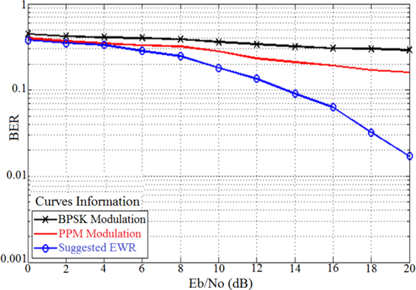
Fig. 11. BER versus Eb/No at 0.5 Gbps in multipath channel model with 1.2 dBm interference at 7 GHz frequency.

Fig. 12. BER versus Eb/No at 0.5 Gbps in multipath channel model without interference at 7 GHz frequency.
IV. CONCLUSIONS
An UWB EMWR with a new architecture has designed and demonstrated. In order to decreasing the interference on NB system at 7 GHz the combination of 8th–8th-order derivative of Gaussian pulse is applied as impulse received signal. This EMWR was designed and modeled in a 90 nm CMOS technology. The all-digital receiver utilizes the PPM-modulated pulses at 7.6 GHz center frequency. Pulse width of the received pulse is about 1.5 ns. The results show that the core chip size is only 0.032 mm2 and the output amplitude pulse is 200 mV peak-to-peak under a supply voltage of 2.2 V. The EMWR consumes 12 pJ/b for data rate of 0.5 Gb/s.
This proposed EMWR can be used in the UWB transceivers. The results showed that the proposed signal decreases the interference with NB system at 7 GHz frequency. The spectrum of the proposed system complies with the FCC's spectrum definition. Moreover, the proposed system obviously provides better performance than other conventional UWB systems in the presence of 7 GHz interference. Hence, the EMWR with obtained results can be used in RF and wireless receiver applications.
 Mohammad Alibakhshi-Kenari was born in 24 February 1988 at Iran. He received the B.S. and M.S. degrees both in the Electrical Engineering, field of Telecommunication from the Islamic Azad University, Najafabad Branch of Esfahan, Iran on February 2010 and the Islamic Republic of Iran, Shahid Bahonar University of Kerman on February 2013, respectively. His researches interests include microwave and millimeter wave circuits, transceivers, radars, antennas and wave propagation, composite right/left-handed transmission lines (CRLH-TLs), metamaterial (MTM) concepts, integrated RF technologies, embedded systems, electromagnetic waves applications, and wireless telecommunication systems. He is now “Editor-in-Chief” in Journal Club for Electronic and Communication Engineering (JCECE) and works as a reviewer in the several good journals such as IEEE Transactions on Industrial Electronics, Elsevier, Taylor & Francis, Wiley, ACES, etc. Mr. M.A-Kenari has too served as a Member of the Technical Program Committee (M-TPC) of some of the international conferences such as APACE 2014, APPEIC 2014, MobiWIS 2014, ICEPIT 2014, CICN 2014, ADVCIT 2014, DPNoC 2015, MobiApps 2015, AR4MET'2015, PIAMSE'2015, etc. So far, he has been published several papers. Also, his Master Thesis entitled “Designing and Fabricating the Ultra Compact and UWB Antennas based on CRLH Metamaterial Transmission Lines with Application in Wireless Radio Transceivers” was approved and granted by Iran Telecommunication Research Center (ITRC) on December 2012 with grant number of 6987/500/T.
 Mohammad Naser-Moghadasi was born in Saveh, Iran, in 1959. He received the B.Sc. degree in Communication Engineering in 1985 from the Leeds Metropolitan University (formerly Leeds polytechnic), UK. Between 1985 and 1987 he worked as an RF design engineer for the Gigatechcompany in Newcastle Upon Tyne, UK. From 1987 to 1989, he was awarded a full scholarship by the Leeds educational authority to pursue an M.Phil. studying in CAD of Microwave circuits. He received his Ph.D. degree in 1993, from the University of Bradford, UK. He was offered then a two years Post Doc. To pursue research on Microwave cooking of materials at the University of Nottingham, UK. From 1995, Dr. Naser-Moghadasi joined Islamic Azad University, Science and Research Branch, Iran-Tehran, where he currently is head of postgraduate studies. His main areas of interest in research are Microstrip antenna, Microwave passive and active circuits, RF MEMS.
Dr. Naser-Moghadasi is member of the Institution of Engineering and Technology, MIET and the Institute of Electronics, Information, and Communication Engineers (IEICE). He has so far published over 140 papers in different journals and conferences.
 Ramazan Ali Sadeghzadeh received his B.Sc. degree in 1984 in Telecommunication Engineering from the Khajeh Nassir Toosi, University of Technology, Tehran, Iran, and M.Sc. degree in Digital Communications Engineering from the University of Bradford and UMIST (University of Manchester, Institute of Science and Technology), UK, as a joint program in 1987. He received his Ph.D. degree in Electromagnetic and Antenna from the University of Bradford, UK, in 1990. He worked as a Post-Doctoral Research assistant in the field of propagation, electromagnetic, antenna, Bio-Medical, and Wireless Communications from 1990 till 1997. From 1984 to 1985 he was with Telecommunication Company of Iran (TCI) working on Networking. Since 1997 he has been with K.N. Toosi University of Technology working with Telecommunications Department at the Faculty of Electrical and Computer Engineering. He has published more than 75 referable papers in international journals and conferences. Dr. Sadeghzadeh's current interests are numerical techniques in electromagnetic, antenna, propagation, radio networks, wireless communications, nano-antennas, and radar systems.
 Aurora Andújar (M′15) was born in Barcelona, Spain, 1984. She received the Bachelor's degree in Telecommunication Engineering specializing in Telecommunication Systems in 2005, the Master degree in Telecommunications Engineering in 2007, the Master of Science in Telecommunication Engineering and Management in 2007, and the Ph.D. degree in 2013 from the Polytechnic University of Catalonia (UPC), Barcelona, Spain. In 2004–2005, she received a research fellowship in the field of Electromagnetic Compatibility from the Signal Theory and Communications Department of the UPC. In 2005, she worked as a Software Test Engineer for applications intended for handset wireless devices. In 2006, she worked as a Software Engineer for Digital Campus in academic environments. From 2007 she joined Fractus as R&D+ I Engineer where she was in charge of the development of technical projects focused on the design of miniature and multiband antennas for wireless devices. She was also involved in the maintenance and growth of the patent portfolio of the company, including the development, writing, and prosecution of new inventions and patents (2007–2013). Since 2009 she is leading research projects in the antenna field for handheld wireless devices in the collaborative university-industry framework. From 2013, she moves to the Products and Service Department and in 2015 she becomes Product Manager of the division where she is in charge of the development and release of new antenna products for wireless devices as well as of leading customer oriented projects. Dr. Andújar has participated in over five national projects and research grants valued over €2 million some of them as principal researcher. She is the author of more than 12 patents in the antenna field. She has published more than 50 papers in scientific journal, international, and national conferences. She has directed more than 15 bachelor and master thesis. She is editor of International Journal on Antennas and Propagation (IJAP).
 Jaume Anguera was born in Vinaròs, Spain, in 1972. He received the Technical Engineering degree in Electronic Systems and Engineering degree in Electronic Engineering, both from the Ramon Llull University (URL), Barcelona, Spain, in 1994 and 1998, respectively, and the Engineering and Ph.D. degrees in Telecommunication Engineering, both from the Polytechnic University of Catalonia (UPC), Barcelona, Spain, in 1998 and 2003, respectively. In 1997–1999 he joined the Electromagnetic and Photonic Engineering Group of the Signal Theory and Communications Department of the UPC as a researcher in microstrip fractal-shaped antennas. In 1999, he was a researcher at Sistemas Radiantes in, Madrid, Spain, where he was involved in the design of a dual-frequency dual-polarized fractal-inspired microstrip patch array for mobile communications. In the same year, he became an Assistant Professor at the Department of Electronics and Telecommunications, URL, where he is currently teaching antenna theory and electromagnetics. Since 1999, he is with Fractus, Barcelona, Spain, where he holds the position of R&D Manager. At Fractus he leaded projects on antennas for base station systems, antennas for automotive and currently managing handset and wireless antenna projects. His current research interests are multiband and small antennas, broadband matching networks, diversity and MIMO antenna systems, electromagnetic dosimetry, genetic optimized antennas, and antennas for wireless devices. From 2003 to 2004, he was with Fractus-Korea (Republic South of Korea) as the leading manager for developing projects in the area of miniature and multiband antennas for handset and wireless applications with Korean companies (Samsung and LG). Since 2001, he has been leading research projects in the antenna field for handset and wireless applications in a frame of Industry–University collaboration: Fractus and Department of Electronics and Telecommunications of Universitat Ramon Llull-Barcelona, Spain resulting in the direction of more than 70 bachelor and master theses, some of them awarded by Spanish institutions and companies. He holds more than 95 granted invention patents (most of them licensed) and 30 more pending patents in the antenna field. He is author of more than 170 journals, international and national and conference papers. He is a Senior Member IEEE. Dr. Anguera has participated in over 15 national projects and research grants valued over €4 million some of them as principal researcher.
Dr. Anguera was a member of the fractal team that in 1998 received the European Information Technology Grand Prize for the fractal-shaped antenna application to cellular telephony. 2003 Finalist to the Best Doctoral Thesis (Fractal and Broadband Techniques on Miniature, Multi frequency, and High-Directivity Microstrip Patch Antennas) on UMTS (prize awarded by Telefónica Móviles España). New faces of Engineering 2004 (awarded by IEEE and IEEE foundation). In the same year 2004, he received the Best Doctoral Thesis in “Network and Broad Band Services” (XXIV Prize Edition “Ingenieros de Telecomunicación”) awarded by Colegio Oficial de Ingenieros de Telecomunicación and the Company ONO. He is reviewer for IEEE Transaction and Antennas and Propagation, IEEE Antennas and Wireless Propagation Letters, IEEE Antennas and Propagation Magazine, Progress in Electromagnetic Research, IEE Electronics Letters, and ETRI journal (Electronics and Telecommunications Research Institute). He is the editor of International Journal on Antennas and Propagation (IJAP). His biography is listed in Who'sWho in the World, Who'sWho in Science and Engineering, Who'sWho in Emerging Leaders and in IBC (International Biographical Center, Cambridge, England).


Target article
Retraction Notice
Related commentaries (6)
A new compact UWB traveling-wave antenna based on CRLH-TLs for embedded electronic systems
Designing an ultra-wideband electromagnetic waves receiver with new architecture for RF and wireless applications
Introducing the new wideband small plate antennas with engraved voids to form new geometries based on CRLH MTM-TLs for wireless applications
Miniaturized printed monopole antenna with applying the modified conductor-backed plane and three embedded strips based on CPW for multi-band telecommunication devices
Modeling and constructing the microstrip notch-loaded rectangular S-shaped patch antennas using L-strip feeding for multi-band frequency performances in the recent wireless telecommunication systems
Significant measureable development of inductance gain per unit of space in loop fractals