I. INTRODUCTION
Multi-port passive networks are a fundamental part of most microwave monolithic integrated circuits (MMICs). They constitute, in fact, power combiners/splitters and impedance matching networks in multi-transistor amplifiers, artificial transmission lines in distributed amplifiers, directional couplers in mixers and balanced amplifiers, and so on.
Although, sometimes difficult and laborious, the characterization of these n-port structures is usually the only way to account for high-frequency effects (e.g. losses, coupling, asymmetries, etc.) that are difficult to simulate using electromagnetic (EM)- or circuit-based models.
Several methods devoted to the characterization of n-port passive structures can be found in the literature. Some of them [Reference Speciale1–Reference Ghiannouchi, Xu and Bosisio5] require special hardware not generally available in many laboratories. Other methods, although based on standard two-port vector network analyzer (VNA) measurements, require auxiliary terminations to be placed at the ports not connected to the VNA during each measurement. Nevertheless, these methods are not easily applicable to on-wafer characterization. In fact, Lu and Chu [Reference Lu and Chu6] require a high number of auxiliary terminations which can be difficult to integrate and, therefore, requires a probe-card which must be calibrated separately. Moreover, the need to perform measurements at each of the port combinations [Reference Lu and Chu6–Reference Reinmann, Kiewitt, Matteus-Kammerer and Pieting10] can be a problem as most structures of interest (e.g. power combiners) have parallel ports with 0° alignment and standard on-wafer probe stations can only measure ports that present a 180° alignment. Furthermore, especially at high frequencies, there is not always enough space to place a coplanar ground-signal-ground (GSG) RF test pad at each port of the network.
On the other hand, this paper presents a complete method for designing and characterizing the test structures, that is, the n-port network to be measured and the associated auxiliary terminations on the same chip that does not require a special calibration routine and, more importantly, does not require all the port combinations being measured. The latter overcomes the problem of non-measurable or difficult-to-measure port combinations. It will be shown that for a given number of ports n, the full scattering parameters matrix (S) of the network can be computed by performing the same number of measurements as other methods which require all the port combinations to be measured. The proposed method allows solving the n-port matrix either analytically in closed form or by numerical optimization. The latter can be straightforwardly implemented in commercial CAD software allowing for better accuracy and robustness of the solution.
The paper is organized as follows: Section II states the general problem of characterizing a linear n-port using a two-port VNA and presents the proposed method for n-port having non-measurable port combinations as well as for networks having some inaccessible ports whereas Section III presents extensive validation results obtained with a nine-port output power combiner and matching network of an X-band MMIC power amplifier. Conclusions are outlined at the end of the paper.
II. THE PROPOSED METHOD
A) Problem statement
In general, an n-port linear network is described by an n × n characteristic matrix, and if reciprocity or symmetry is not assumed, there will be n Footnote 2 elements of the matrix to be determined. In order to characterize the n-port using a standard two-port VNA, methods in the literature require performing two-port measurements for every possible combination of two ports of the n-port. The two-port measurements are performed while the n−2 ports not connected to the VNA are terminated with appropriate loads. For each two-port measurement a 2 × 2 sub-matrix of the characteristic matrix of the n-port is determined. The nature of the determined sub-matrix will depend on the type of auxiliary termination used (e.g. if 50 Ω is used a scattering (S2×2) sub-matrix will be determined, whereas an impedance (Z2×2) sub-matrix will be obtained if perfect open circuits are used). Once all the ![]() two-port combinations are measured the full n-port characteristic matrix is obtained by picking its elements from the measured 2 × 2 sub-matrices.
two-port combinations are measured the full n-port characteristic matrix is obtained by picking its elements from the measured 2 × 2 sub-matrices.
The main drawback of this procedure is that in practice it is not always possible to perform measurements between all the ports of a network, whether due to on-wafer probe-station limitations that preclude the simultaneous measurement of ports that do not have the right alignment, or due to geometric limitations that prevent the insertion of an RF GSG test pad at each port, thus preventing such ports to be contacted at all.
The proposed method aims to solve both problems. The first and the most common one regards n-port networks where all ports are measurable (i.e. all ports have their corresponding RF access pad so that the RF probe can be connected to it) but there are some two-port combinations which are not measurable (this is normally the case on power combiners where ports on the same side of the network cannot be measured together). The second problem regards the case in which the available area is not enough for an RF test pad to be placed in the test structure, thus making some ports not measurable at all. As will be shown in the next subsection the proposed method overcomes these problems without increasing the number of measurements with respect to other methods.
B) Non-measurable two-port combinations
Let us assume that we have an n-port for which ports i and port j cannot be measured with a two-port VNA because of the n-port pattern, and that there is also a third port k for which the two-port measurements i−k and j−k are realizable. As will be demonstrated, by performing the three two-port measurement shown in Fig. 1, it is possible to compute the non-directly measurable i − j transmission parameter.

Fig. 1. Measurement sequence for the identification of non-measurable port combinations.
In fact, the 2 × 2 matrix measured by the VNA (Sm) can be easily transformed to its equivalent representation in terms of the impedance matrix (Zm):
Thus, from measurements A and B in Fig. 1, the Zik and Zjk sub-matrices are, respectively, obtained. It should be noted that these are 2 × 2 sub-matrices of the Z matrix of the n-port and thus their elements are Z ii, Z ik, Z ki, Z kk, Z jj, Z jk, and Z kj, elements of the full characteristic matrix of the n-port (Z).
In the same way, measurement C in Fig. 1 transformed to Z representation will provide the following equations:
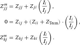
In (2) I i and I j are the currents at ports i and j, ![]() and
and ![]() are the parameters obtained by transforming to Z domain the VNA measurements corresponding to measurement C, and Z Term is the auxiliary impedance used to terminate port i.
are the parameters obtained by transforming to Z domain the VNA measurements corresponding to measurement C, and Z Term is the auxiliary impedance used to terminate port i.
Rearranging (2) and taking into account that Z ii, Z ik, Z ki, Z kk, Z jj, Z jk, and Z kj are known from the previous measurements a final expression for the unknown Z ij and Z ji can be found:

Thus, for any combination of ports i, j, k where ports i and j cannot be measured together, it is possible to obtain the non-directly measurable transmission parameters Z ij and Z ji by using (3). This means that for any pair of non-directly measurable parameters Z ij and Z ji in the network an additional measure is needed.
Moreover, it can be noticed that for reciprocal ports, Z Term need not be measured in order to determine Z ji in (3) (or Z ij = Z ji). In fact, Z Term can be determined from the second part of (3) after calculating Z ji.
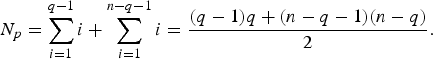
In order to calculate the number of measurements that are needed to determine the full Z matrix, let us consider an n-port network where there are two sets of ports composed respectively by q and n − q elements and that ports belonging to the first set cannot be measured simultaneously and the same is valid for the second set (e.g. there are q elements on the input side of the structure and n − q on the output). So, once all the ![]() practicable two-port measurements are performed (○), the non-directly measurable elements of the matrix (Δ and □) will be disposed as in Fig. 2.
practicable two-port measurements are performed (○), the non-directly measurable elements of the matrix (Δ and □) will be disposed as in Fig. 2.

Fig. 2. Matrix for the calculation of the number of required measurements.
As can be observed in Fig. 2 the number of pairs of non-directly measurable elements of the matrix (N p) will be given by
Then, the total number (M) of measurements required by the method will be given by
Thus, this method solves the problem of the non-directly measurable port combinations without increasing the number of measurements with respect to other methods [Reference Lu and Chu6, Reference Lu and Chu8–Reference Reinmann, Kiewitt, Matteus-Kammerer and Pieting10].
C) Non-measurable ports
In order to deal with ports that are not measurable at all, a third auxiliary termination is required.Footnote 1
Let us assume a reciprocal n-port (this is normally the case for most passive structures) having some non-measurable ports and select three ports of the network i, j, and k, where ports i and j are measurable and port k is not. By performing the measurements shown in Fig. 3 and transforming the results to Z domain the following equations are obtained:


Fig. 3. Measurements required for the identification of non-measurable ports.
In (6) the “x” superscript must be set to B or C Footnote 2 according to the measurements indicated in Fig. 3. Solving the system of equations in (6) and taking into account the network reciprocity results in the following expressions for the coefficients of the non-measurable port k Footnote 3:

This procedure can be applied to any other non-measurable port r Footnote 4 and (7) be used to obtain Z ir and Z jr. Then Z rk can be obtained by performing an additional measurement between ports i and j with ports r and k terminated on Z B and using the following equation:

In (8), Z m are the measured values with both ports r and k terminated on Z B. It can be noticed that the total number of measurements required is still the same as in Section II.B. However, when the network has more than two non-measurable ports, the number of necessary measurements becomes higher since also the cross terms between these non-measurable ports need to be determined.
D) Numerical solution using a CAD software
Although (3), (7), and (8) give closed-form solutions for the elements of the characteristic matrix Z, they are based on the assumption of ideal auxiliary terminations. In fact, since the method considers the Z matrix, ideal open-circuit terminations are assumed.Footnote 5 At high frequencies when the impedance of the unconnected test port is not high enough to be considered as an open circuit, the closed-form expressions cannot be evaluated directly and therefore a numerical procedure is required. In practice, the analytical solution can be used as a starting point to obtain a more accurate and robust solution using numerical optimization with the real (i.e. measured) auxiliary terminations (open and Z Term). This can be done straightforwardly in most high-frequency CAD tools by minimizing with a suitable algorithm (e.g. gradient) an error function defined as the least-square discrepancies between the measured and the simulated S parameters of the network for all the test configurations. The unknown elements of the S matrix are, in this case, the optimization variables.
Moreover, although the identification of a complex nine-port structure such as the one presented in the next section has been performed using the minimum number of measurements required by the method, a CAD-based optimization approach can be easily set up in order to take advantage of extra or redundant measurements, making the method more robust and reducing uncertainty.
III. EXPERIMENTAL RESULTS
The proposed method was applied to the characterization of a nine-port passive network. The structure, shown in Fig. 4, is the output power combiner and impedance matching network of a 10 W X-band MMIC high-power amplifier (HPA) built in GaInP/GaAs Power HBT Technology.

Fig. 4. Nine-port output power combiner and matching network of an X-band MMIC HPA used for the validation of the method.
Ports 1–8 at the bottom correspond to the inputs of the power combiner where the eight power cells of the HPA are connected, whereas port 9 is the output of the HPA where a 50 Ω load is normally connected. Since the RF pads of ports 1–8 have all the same orientation, it is not possible to contact them with a standard on-wafer probing system (i.e. a system having 180° between probes) without one of the probes being above the structure. In fact, at high frequencies spurious coupling between the probe and the underlying lines can affect the measurement. Therefore, the proposed method is specially suitable since it allows to fully characterize this kind of structure without having to measure the transmission S parameters for all the combinations of ports 1–8 on the bottom of the combiner: it is only required that transmission and reflection parameters be measured between each port at the bottom (1–8) and the port at the top (9). Moreover, being the network symmetrical along the central vertical axis, only ports 1, 3, 5, and 7 need to be measured since ports 8, 6, 4, and 2 show symmetrical behavior. Hence, in order to apply the method, a total of 20 S-parameter measurements in the range 1–25 GHz were performed using an Agilent E8364C 2-port VNA, a Cascade on-wafer probe station, and GSG RF probes with 150 µm of pitch, according to the matrix in Fig. 5.

Fig. 5. Measurement matrix (P1 and P2 (VNA ports), O open circuit, Z = Z Term).
The auxiliary terminations Z Term were 50 Ω resistors grounded through a via hole and connected to the ports with gold bond wires whereas the “Open” circuit standard was a coplanar-to-microstrip transition pad followed by 76 µm of a 50 Ω microstrip line. Both Z Term and the open standard were characterized separately with one-port S-parameter measurements. After the measurements were performed, the ![]() matrix of the nine-port network was determined at each frequency using (3).
matrix of the nine-port network was determined at each frequency using (3).
Figure 6 show which elements of the Z matrix were identified by each of the 20 measurements indicated in Fig. 5.

Fig. 6. Scheme of the independent elements of the reciprocal and symmetrical Z matrix identified by each measurement of Fig. 5.
However, since the open termination was not ideal as assumed in (3), an optimization routine was implemented in ADS CAD software to determine Z by minimizing the least-squares discrepancies between the measured and modeled S parameters in all the configurations of the matrix in Fig. 5, using ![]() as a starting point for Z, and the measured auxiliary terminations.
as a starting point for Z, and the measured auxiliary terminations.
Figure 7 shows the comparison between some of the reflection and transmission S parameters of the network determined with the method and the corresponding values obtained both with an S-parameter simulation of the structure using circuit-based models, as well as with a 2.5D EM simulation using the method of moments. As can be seen from Fig. 7, there is very good agreement between the parameters obtained with the proposed method and those obtained with EM simulation. It can also be noticed that circuit-based models give accurate results up to 5 GHz but fail to predict the high-frequency resonances of the structure at ~11 GHz.

Fig. 7. S11 and S12 of the network: method (symbols), EM simulation (thick line), circuit-based model (thin line).
In order to obtain good EM simulation results several time-consuming reverse-engineering operations were performed using separate ad hoc structures not shown here. In fact, it was necessary to adjust the values of the substrate properties for this particular foundry run, which slightly differed from the nominal values given by the foundry. Moreover, since a 2.5D EM simulator was employed (i.e. not a full 3D simulator), also the geometry and mesh settings of the simulator had to be carefully validated using the ad hoc structures.
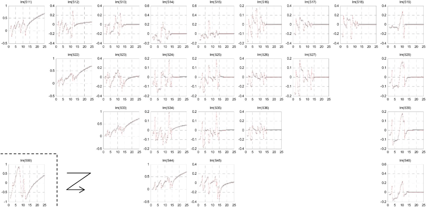
Figures 8 and 9 show the real and imaginary parts of all the independent parameters of the full 9 × 9 S matrix for the EM-simulated matrix and the matrix obtained with the proposed method. In fact, although the n-port characteristic matrix has 81 elements, network reciprocity and geometrical symmetry of ports 1–4 with respect to ports 5–8, results in the S matrix being fully characterized by only 25 independent elements. It can be observed that there is very good agreement also for the rest of the elements of the S matrix of the network.

Fig. 8. Real part of the independent S parameters of the network obtained with the proposed method (symbols) and EM simulation (thick line).

Fig. 9. Imaginary part of the independent S parameters of the network obtained with the proposed method (symbols) and EM simulation (thick line).
Figures 10 and 11 allow comparing two magnitudes of the n-port combiner that depend on the full S matrix of the n-port: the common-mode impedance seen when applying a common mode excitation to ports 1–8, and the associated attenuation from each of ports 1–8 to port 9. As can be seen from these figures, although the results seem to be a little noisier, the method gives very close results to the EM simulation.

Fig. 10. Common mode impedance of the combiner: method (symbols), EM simulation (thick line), circuit-based model (thin line).

Fig. 11. Combiner attenuation for common mode excitation at ports 1–8: method (symbols), EM simulation (thick line), circuit-based model (thin line).
In order to evaluate quantitatively the difference between the two S parameter matrices plotted in Figs 8 and 9, it is necessary to define an error matrix ΔS, and to calculate a suitable metric or norm on it. Accordingly, we define each element of ΔS:
as the distance between two corresponding complex-valued elements of the S matrices obtained with the proposed method (![]() ) and with the EM simulation (SEM). Since we are dealing with a reciprocal and symmetrical matrix, only the N independent elements of the matrix need to be considered, that is, the ones in Fig. 6. It is therefore convenient to group them into an error vector
) and with the EM simulation (SEM). Since we are dealing with a reciprocal and symmetrical matrix, only the N independent elements of the matrix need to be considered, that is, the ones in Fig. 6. It is therefore convenient to group them into an error vector ![]() containing the independent elements of
containing the independent elements of ![]() . Since S parameters are already normalized magnitudes with respect to the reference impedance and have magnitudes that for passive networks can vary from 0 to 1, an absolute error definition is considered and therefore the average distance or error between the two matrices can be simply evaluated by calculating the root mean square value of the error vector, namely:
. Since S parameters are already normalized magnitudes with respect to the reference impedance and have magnitudes that for passive networks can vary from 0 to 1, an absolute error definition is considered and therefore the average distance or error between the two matrices can be simply evaluated by calculating the root mean square value of the error vector, namely:

where N is the number of independent elements of the S matrix (Fig. 6). The scattering matrix being frequency dependent, also the error matrix and its norm needs to be evaluated at each frequency. Figure 12 shows the plot of the error metric ![]() and, for the sake of comparison, also the discrepancy measured by the same metric between the circuit-based model of the network and the EM simulation (
and, for the sake of comparison, also the discrepancy measured by the same metric between the circuit-based model of the network and the EM simulation (![]() ).
).

Fig. 12. Error metric between the S matrix obtained with EM simulation and the one obtained with the method (![]() ), and between the EM matrix and the circuit simulation (
), and between the EM matrix and the circuit simulation (![]() ).
).
As can be seen from Fig. 12, the average error distance between the S matrix obtained with the method and the EM-simulation is much smaller than the one between a circuital model and the EM simulation.
It is also interesting to calculate the error between some sub-matrices of the S matrix that were measured directly (i.e. terminating the remaining seven ports not connected to the VNA with 50 Ω loads) and the corresponding values obtained with the EM simulation. Accordingly, Fig. 13 displays the metric for the 2 × 2 sub-matrices obtained with port 2 of the VNA connected to port 9 of the n-port, and port 1 of the VNA connected to ports 1, 3, 5, and 7 of the network.

Fig. 13. Error between some 2 × 2 sub-matrices of the S matrix of the network measured directly and the corresponding matrices obtained with EM simulations.
It can be observed that the error metrics for these measurements, which were not used for the identification of the n-port, are comparable and in some cases somewhat higher than the errors obtained with the proposed method. The latter may be due to the fact that imperfect 50 Ω loads were employed for the direct measurement of the S sub-matrices but also to the fact that each element of the ![]() matrix obtained with the method is based on several two-port measurements and thus the method has some averaging properties that reduce random measurement errors.
matrix obtained with the method is based on several two-port measurements and thus the method has some averaging properties that reduce random measurement errors.
IV. CONCLUSIONS
The paper presented a simple method for the characterization of n-port linear networks using a standard two-port VNA. The method is completely general and in principle can be applied to any passive multi-port network. The main advantages of the method are that it does not require all the two-port combinations to be measured and that it can also deal with non-measurable port combinations. In fact, it is not unusual for circuit ports to have orientations different from the standard 180° or to have ports that due to geometrical constrains cannot be contacted at all. Still, this method can solve for this non-measurable combinations by repeating measurements at the allowed port combinations. The method was applied to the full linear characterization of a nine-port microstrip power combiner and matching network and extensively validated against circuit-based as well as EM simulations with very good results. Although the proposed method and EM simulations give similar results, accurate and reliable EM simulations require significant expertise and are normally more time consuming than the proposed method, considering that some sort of trial and error experimental validation will also be required for the EM simulation tool.
ACKNOWLEDGEMENTS
The authors are grateful to the anonymous reviewers for their useful comments and suggestions.
 Julio A. Lonac was born in La Plata, Argentina in 1976. He received the M.S. degree in electronics from the UNLP (University of La Plata, Argentina) in 2001, and the Ph.D. degree in electronics, informatics and telecommunications from UNIBO (University of Bologna, Italy) in 2005. His major field of study regards the modeling and design of MMIC for telecommunication and radar applications. He worked as a research fellow at the University of Ferrara from 2006 to 2007, and for CoRiTel (Research Consortium composed of Ericsson Lab Italy, ITS and four universities – Rome, Bologna, Salerno, and Milano.) from 2007 to 2008. He collaborated as an MMIC designer in the ASI (Italian Space Agency) and CONAE (Argentinean Space Agency) SAOCOM project. He worked as an MMIC designer with MEC srl from 2008 to 2011. He is currently an MMIC designer with Huawei.
 Ilan Melczarsky received the M.Sc. degree (cum laude) in electronics engineering from the University of Mar del Plata, Buenos Aires, Argentina, in 2000, and the Ph.D. degree in electronics and computer science from the University of Bologna, Bologna, Italy in 2005. From 2000 to 2001, he has been a senior product engineer with Ericsson Argentina. Since 2005, he has been with the Dipartimento di Ingegneria Elettronica (DEIS), University of Bologna, as a post-doctoral researcher and teaching assistant. His research interests include non-linear characterization and modeling of high-frequency electron devices and circuits, and high-frequency circuit design. Dr. Melczarsky was a fellow of the Italian Research Council (CNR) from 2002 to 2005.
 Rudi Paolo Paganelli received the Dr. Eng. degree in electrical engineering in 1998 and the Ph.D. degree in electrical engineering, computer science and telecommunications in 2002 from the University of Bologna (Italy). In 2002, he joined the CNR-IEIIT in Bologna as a research fellow and from 2003 he has been as assistant professor for the power electronics course at the University of Bologna (Italy). His research interests include electronic device modeling, microwave circuit design, non-linear circuits, and power electronics.