I. INTRODUCTION
With the rapid advancement in wireless technology printed monopole antennas have generated keen interest among the researchers worldwide as they have high-gain, high-efficiency, omnidirectional radiation pattern, and robustness. U, E, Elliptical, and Rectangular slots have been introduced for bandwidth enhancement of the microstrip patch antenna [Reference Wong1–Reference Telsang and Kakade5]. A wide slot antenna fed by microstrip line with fork-like tuning stub is presented [Reference Sze and Wong6]. Bandwidth enhancement is achieved by properly adjusting the parameters of the fork-like tuning stub. T, E, U, and ring shaped slots has been introduced in patch to obtain band notch characteristics [Reference Rezaeieh and Abbak7–Reference Ojaroudi and Ojaroudi10]. Bandwidth enhancement of a printed slot antenna is reported by rotating the slot to an appropriate angle [Reference Jan and Su11]. A pair of parasitic strip lines is used in slot antenna [Reference Jan and Wang12] to achieve 80% fractional bandwidth and miniaturization of about 70%. Bandwidth enhancement has been proposed by introducing a parasitic patch in slot antenna [Reference Sung13]. Higher-order modes are excited due to introduction of the parasitic patch. A pair of parasitic patches, curved slots, and EBG structure has been introduced in a slot antenna for bandwidth enhancement [Reference Fan, Yen, Lee, Hu and Yang14, Reference Guo, Tian, Wang, Luo and Ji15]. Radial slots have been proposed for the dual-frequency operation [Reference Chen and Hsu16], where the operating frequency can be controlled by varying the angle between the slots.
This paper presents a simple broadband planar monopole microstrip patch antenna with curved slot and partial ground plane. Initially by adding a rectangular slot the bandwidth of the monopole antenna is enhanced due to excitation of higher-order modes and on blending the corners of the slot, the impedance bandwidth is further enhanced due to impedance matching. Partial ground plane plays a crucial role in the impedance matching, as the size of the ground plane is increased capacitive effect has been observed. The proposed antenna shows 109% fractional bandwidth. Stable radiation pattern throughout the operating band has been observed.
II. ANTENNA DESIGN
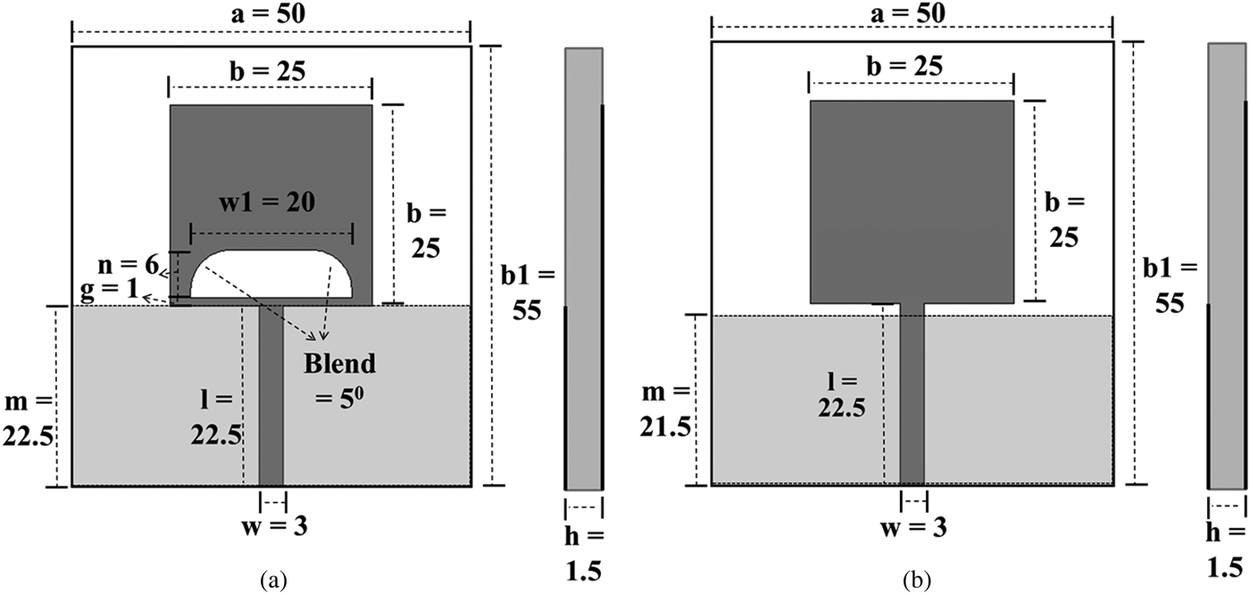
The configuration of the proposed planar monopole microstrip patch antenna and simple monopole antenna is shown in Fig. 1. Both antennas have overall dimensions of 50 × 55 mm2 and are printed on the FR4 dielectric substrate having relative permittivity ε r = 4.3 and loss tangent of 0.025. The thickness of the dielectric substrate is 1.5 mm and 50 Ω microstrip lines with 3 mm width are used to feed both antennas. The patch and microstrip line are printed on one side of the substrate and the partial ground plane is printed on the other side. The length of the microstrip line is denoted by l. The distance between the curved slot and the edge of the patch is denoted by g. This gap is optimized for better impedance matching. A curved slot has been introduced in the patch to achieve bandwidth enhancement.

Fig. 1. Geometrical configurations of (a) the proposed antenna and (b) simple monopole antenna. (all dimensions are in mm)
The length of the microstrip line and the length of the partial ground plane are kept same for obtaining the best possible impedance matching. Exact values of the different parts of the proposed antenna are mentioned in Fig. 1. Simulation is carried out using CST simulation software, a finite integration technique (FIT)-based commercial electromagnetic simulator. In this design, to enhance the bandwidth a curved slot has been introduced in the patch of the simple monopole antenna. Initially a rectangular slot with dimension n × w1 has been introduced to enhance bandwidth. Two corners of the rectangular slots are blended to 5° for further bandwidth enhancement. Signals are radiated from the patch as well as from the ground plane. From the simulated results, it is found that the proposed antenna has achieved bandwidth enhancement of about 2.2 GHz as compared with the simple monopole antenna.
III. PARAMETER STUDY
In this section, the study of various parameters of the proposed antenna is carried out to understand their effect and to find out the best possible design parameters. Figure 2 shows the simulated return loss of the simple monopole antenna without curved slot and the proposed antenna. It is observed that the impedance bandwidth of the simple monopole antenna and the proposed antenna is 83% (1.9–4.6 GHz) and 109% (2–6.8 GHz), respectively. All other parameters are same for both the cases except the introduction of curved slot in the proposed design and the gap between the edge of the patch and the ground plane as shown in Fig. 1.
Fig. 2. Simulated return loss of simple monopole antenna and the proposed antenna.
Simulated return loss of the proposed antenna with various values of the ground plane (value = m) is shown in Fig. 3. Size of the ground plane actually shows the gap between the edge of the patch and the ground plane. It has been observed that as this gap is increased the bandwidth of the proposed antenna is degraded due to impedance mismatch. Return loss graph clearly shows that on increasing this gap either in upward direction or downward directions drastically affects the return loss. So the optimized value of the ground plane is kept as 22.5 mm, which shows that there is no gap between the edge of the patch and the ground plane as shown in Fig. 1.
Fig. 3. Simulated return loss of proposed antenna with various values of m. (other parameters are same as in Fig. 1)
Effects of various values of w1 and n are shown in Figs 4 and 5, respectively. It is obvious from the results that as the values of w1 and n are increased the bandwidth of the proposed antenna increases. The lower resonant frequency f 1 (2 GHz) is nearly constant and is same as that of simple monopole antenna but on increasing the values of w1 and n, the upper resonant frequency f 2 is increased, due to excitation of higher-order resonating modes. On increasing the respective sizes the upper resonant frequency f 2 increases till n reaches to 6 mm and w1 reaches to 20 mm, after that upper resonant frequency f 2 starts degrading due to impedance mismatch. So the optimized values of w1 and n are set to 20 and 6 mm, respectively.
Fig. 4. Simulated return loss of proposed antenna with various values of w1. (other parameters are same as in Fig. 1)
Fig. 5. Simulated return loss of the proposed antenna with various values of n. (other parameters are same as in Fig. 1)
After introduction of the rectangular slot two edges are blended. Figure 6 shows simulated return loss with various values of blending (value = deg). As the value of deg is increased the lower resonant frequency f 1 remains constant but the upper resonant frequency f 2 is increased due to better impedance matching. It is observed that the upper resonant frequency f 2 has enhanced from 6.5 to 6.8 GHz, showing bandwidth enhancement of 0.3 GHz. The optimized value of deg is set to 5°. In the next section, various results obtained after simulation and measurement are described and elaborated.
Fig. 6. Simulated return loss of the proposed antenna with various values of deg (other parameters are same as in Fig. 1.)
IV. RESULTS
The prototype of the proposed antenna is fabricated using LPKF PCB prototyping machine as shown in Fig. 7 and the return loss has been measured using Agilent Vector Network Analyzer. Figure 8 shows measured and simulated return loss of the proposed antenna. The measured and simulated results are in good agreement which validates the simulation process. Measured impedance bandwidth of the proposed antenna is 109% (2–6.8 GHz). Simulated gain comparison of simple monopole antenna and proposed antenna is shown in Fig. 9. The peak gain of the proposed antenna is 4.8 dB. Gain enhancement of about 0.6 dB can be observed in 5.2–6.2 GHz range, whereas there is slight deviation of about 0.3 dB at other operating frequencies.
Fig. 7. Photograph of the fabricated antenna. (a) Top view. (b) Bottom view.
Fig. 8. Simulated and measured return losses of the proposed antenna.
Fig. 9. Simulated gain of simple monopole antenna and proposed antenna.
Simulated surface current distribution of the proposed antenna is demonstrated in Fig. 10. From the current distribution it is imminent that due to introduction of the curved slot the current path is diverted. As a result higher-order modes are excited and signals starts radiating from the edges of the slot. It is clear that at higher frequencies the current distribution is changed and the peak values are higher as compared with lower frequencies. Peak values of the surface current and the current distribution for various frequencies at constant phase (226°) is shown in Fig. 10. Stable radiation pattern has been observed across the operating bandwidth. Figure 11 shows simulated and measured E- and H-plane radiation patterns of the proposed antenna at various frequencies. Simulated and measured results are in good agreement, validating the simulation process. Omnidirectional H-plane and bidirectional E-plane radiation pattern has been observed which are generally required for monopole antenna.
Fig. 10. Simulated surface current distribution of the proposed antenna at (a) 2.4 GHz, (b) 3.5 GHz, (c) 5.2 GHz, and (d) 5.5 GHz.
Fig. 11. Simulated and measured radiation pattern of the proposed antenna at (a) 2.4 GHz, (b) 3.5 GHz, (c) 5.2 GHz, and (d) 5.5 GHz.
V. CONCLUSION
A simple broadband planar monopole microstrip patch antenna with curved slot and partial ground plane is proposed. Bandwidth enhancement has been achieved by cutting a curved slot in the patch of the antenna due to excitation of higher-order modes and better impedance matching. From the results obtained in this study, the impedance bandwidth of the proposed antenna determined by 10 dB return loss is 109%, which shows broadband nature and bandwidth enhancement of 26% in comparison with the simple monopole antenna. The gain of the proposed structure is maintained as compared with the simple monopole antenna with slight deviation of about 0.3 dB in the operating band. The proposed antenna exhibits stable radiation pattern over the entire operation frequency range. This suggests that the proposed antenna is useful for 2.4/5.2/5.8-GHz WLAN bands, 2.5/3.5/5.5-GHz WiMAX bands, and other wireless communication services.
Sudeep Baudha received his B.E. degree in Electronics and Communication Engineering from Rajiv Gandhi Proudyogiki Vishwavidyalaya, Bhopal (India) in 2007 and received his M.Tech. degree in Radio Frequency and Microwave Engineering from Indian Institute of Technology, Kharagpur (India) in 2009. He has been pursuing his Ph.D. degree from Indian Institute of Information Technology Design and Manufacturing (IIITDM), Jabalpur (India) since 2012. His fields of interest are microstrip antenna, planar antenna, microwave communication, etc.
Dr. Dinesh Kumar Vishwakarma is an Associate Professor of Electronics and Communication Engineering at Indian Institute of Information Technology Design and Manufacturing (IIITDM), Jabalpur, India. He received his Ph.D. degree in Electrical Communication Engineering from Indian Institute of Science, Bangalore in 2005. He was a visiting foreign researcher in Japan from 2006 to 2009. Prior to this, he was employed in Ministry of Communication & IT through Indian Engineering Services. His research interests include computational electromagnetics, microwave circuits, antenna and wave propagation, photonics, and optical communication.