


I. INTRODUCTION
With the recent advances in wireless communication industry, there is an increasing demand for smaller antennas that can be easily integrated in monolithic microwave integrated circuits [Reference Sumantyo, Ito and Takahashi1]. Among various types of planar antennas, the microstrip antenna provides all of the advantages of printed circuit technology. This antenna consists of a radiating patch on one side of a dielectric substrate; the patch is generally made of conducting material such as copper or gold and can take any possible shape. They have some drawbacks such as low radiation efficiency [Reference Helszajn and James2]. High T c superconducting materials (HTS's) provide flexibility and accuracy in integrated circuit design, and can be used to overcome radiation efficiency of antennas [Reference Hansen3–Reference Cai and Bornemann6]. The triangular microstrip antenna (TMA) is one of the most preferable for small equipment; it has the advantage of occupying less metalized area on the substrate than other existing configurations [Reference Dahele and Lee7–Reference Guha and Siddiqui15]. However, this will produce even lower gain and smaller bandwidth. An equilateral triangular microstrip antenna (ETMA) has a larger bandwidth compared to other triangular antenna.
Many techniques of bandwidth enhancement have been suggested and designed. Bandwidth of antenna can be increased by using the thick substrate of low dielectric constant or by designing the antenna in a multilayered media [Reference Biswas and Guha9–Reference Staraj, Cambiaggio and Papiernik11]. By introducing the air gap, we can obtain the tunable resonant frequency characteristics; it is possible to increase the bandwidth. The air gap idea, that an air gap between the substrate and the ground plane has been proposed by Lee and Dahele [Reference Dahele and Lee7]. Recently, there have been a number of investigations of resonant frequencies of tunable equilateral triangular microstrip patch antennas. These investigations are based on the transmission-line model and the cavity model in simple computer aided design formulas for determining the tunable frequencies [Reference Biswas and Guha9, Reference Guha and Siddiqui15]. However, the accuracy of these approximate models is limited and only suitable for analyzing simple, regularly shaped antenna or thin substrates. The full-wave spectral domain technique is extensively used in microstrip analysis and design [Reference Nachit and Foshi12, Reference Dreher16, Reference Das and Pozar17]. This method gives better results than approximate techniques. In the current paper, we have developed an analytical model for analysis of high T c superconducting triangular microstrip antenna (HTSTMA) with two lower substrates of which little has been published. Our theoretical study is carried out by using a full-wave spectral domain technique in conjunction with the complex resistive boundary condition.
II. THEORETICAL MODEL
A) Geometrical structure
The air gap tuned HTSTMAs considered in this work are shown in Fig. 1. It was obtained by depositing a high T c superconducting patch on a dielectric layer, which is mounted on air layer. This last layer is printed on the grounded plane. The upper layer being the dielectric substrate material is taken to be isotropic, has a uniform thickness of d 2. The lower layer being the air gap of thickness d 1 has relative permittivity equal to 1. The high T c superconducting triangular patch has thickness t, and side length W.

Fig. 1. Geometry of air gap tuned HTSTMA.
B) Theory
In this subsection, the full-wave spectral domain approach is used for analysis and design of an air gap tuned HTSTMAs. In this approach, starting from Maxwell's equations in the spectral domain, the general equations of the electric and magnetic transverse fields inside the j layer can be written as [Reference Bouttout, Benabdelaziz, Fortaki and Khedrouche18]
 $$\eqalign{&\bar E\lpar r_s\comma \; z\rpar =\left[\matrix{ {E_x \lpar r_s\comma \; z\rpar } \cr {E_y \lpar r_s\comma \; z\rpar } \cr } \right]\cr &={1 \over {4\pi ^2 }}\vint_{ - \infty }^{+\infty } \vint_{ - \infty }^{+\infty } \bar F\lpar k_s\comma \; r_s \rpar \, \tilde{\bar{e}}\lpar k_s\comma \; z\rpar dk_x \, dk_y \comma \;}$$
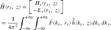 $$\eqalign{&\bar H\lpar r_s\comma \; z\rpar =\left[\matrix{ {H_y \lpar r_s\comma \; z\rpar } \cr { - E_x \lpar r_s\comma \; z\rpar } } \right]\cr &={1 \over {4\pi ^2 }}\vint_{ - \infty }^{+\infty } \vint_{ - \infty }^{+\infty } \bar F\lpar k_s\comma \; r_s \rpar \, \tilde {\bar {h}}\lpar k_s\comma \; z\rpar dk_x \, dk_y \comma \;}$$
Where
 $$\bar F\lpar k_s\comma \; r_s \rpar ={1 \over {k_s }}\left[{\matrix{ {k_x } & {k_y } \cr {k_y } & { - k_x } \cr } } \right]e^{ik_s \cdot r_s }\comma \;$$
With
 $$k_s=k_x \, \hat x+k_y \, \hat y\comma \; \quad r_s=x\, \hat x+y\, \hat y\comma \;$$
The superscripts of e and h in (1) and (2) denote the TM and TE waves, which are defined as
 $$\tilde {\bar {e}}\left({k_s\comma \; z} \right)=\bar{\bi A}_j e^{ - i\, k_{zj} z}+\bar{\bi B}_j e^{i\, k_{zj} z}\comma \;$$
 $$\tilde {\bar {h}}\left({k_s\comma \; z} \right)=\lpar \bar{\bi A}_j e^{ - i\, k_{zj} z} - \bar{\bi B}_j e^{i\, k_{zj} z} \rpar \cdot \bar g_j \lpar k_s \rpar \comma \;$$
with
 $$\bar g_j=\left\vert {\matrix{ {\displaystyle{{\omega \varepsilon _0 \varepsilon _j } \over {k_{zj} }}} & 0 \cr 0 & {\displaystyle{{k_{zj} } \over {\omega \mu _0 }}} \cr } } \right\vert \comma \;$$
where A j and B j are unknown vectors.
Writing (4) and (5) at the interfaces of the layer (Fig. 2), and by eliminating the unknowns A j and B j, we obtain the matrix form

Fig. 2. Geometry of layers.
 $$\left[{\matrix{ {{\bi \tilde {\bar {e}}}\left({k_s\comma \; z_j^ - } \right)} \cr {{\bi \tilde {\bar {h}}}\left({k_s\comma \; z_j^ - } \right)} \cr } } \right]=\bar{\bi T}_j \, \left[{\matrix{ {{\bi \tilde {\bar {e}}}\left({k_s\comma \; z_{j - 1}^+} \right)} \cr {{\bi \tilde {\bar {h}}}\left({k_s\comma \; z_{j - 1}^+} \right)} \cr } } \right]\comma \;$$
With
 $$\bar T_j=\left[{\matrix{ {\bar I\cos \lpar \bar k_{zj} d_j \rpar } & { - i\bar g_j^{ - 1} \left({k_s } \right)\sin \lpar \bar k_{zj} d_j \rpar } \cr { - i\bar g_j \left({k_s } \right)\sin \lpar \bar k_{zj} d_j \rpar } & {\bar I\cos \lpar \bar k_{zj} d_j \rpar } \cr } } \right]\comma \;$$
Where  $\bar I$ being the (2 × 2) unit matrix and
  $\bar k_{zj} $ is given by
 $$\bar k_{zj}=\left\vert {\matrix{ {k_{zj} } & 0 \cr 0 & {k_{zj} } \cr } } \right\vert .$$
The relation between the tangential electric and magnetic field components in dielectric layers below the patch interface is given by
 $$\left[{\matrix{ {{\bi \tilde {\bar {e}}}\left({k_s\comma \; z_M^ - } \right)} \cr {{\bi \tilde {\bar {h}}}\left({k_s\comma \; z_M^ - } \right)} \cr } } \right]=\bar{\bi T}_1 \; \bar{\bi T}_2 \; \bar{\bi T}_3 \ldots \bar{\bi T}_M \; \left[{\matrix{ {{\bi \tilde {\bar {e}}}\left({k_s\comma \; 0} \right)} \cr {{\bi \tilde {\bar {h}}}\left({k_s\comma \; 0} \right)} \cr } } \right].$$
Above the patch interface, the relation between the tangential electric and magnetic field components in dielectric layers is given by
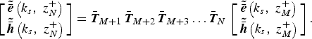 $$\left[{\matrix{ {{\bi \tilde {\bar {e}}}\left({k_s\comma \; z_N^+} \right)} \cr {{\bi \tilde {\bar {h}}}\left({k_s\comma \; z_N^+} \right)} \cr } } \right]=\bar{\bi T}_{M+1} \, \bar{\bi T}_{M+2} \, \bar{\bi T}_{M+3} \ldots \bar{\bi T}_N \, \left[{\matrix{ {{\bi \tilde {\bar {e}}}\left({k_s\comma \; z_M^+} \right)} \cr {{\bi \tilde {\bar {h}}}\left({k_s\comma \; z_M^+} \right)} \cr } } \right].$$
We can put the product matrix as
 $$\bar{\bi \Gamma}_ \lt=\mathop {\bf \Pi} \limits_{j=M}^1 \bar{\bi T}_j=\left[{\matrix{ {{\bf \Gamma} _ \prec ^{11} } & {{\bf \Gamma} _ \prec ^{12} } \cr {{\bf \Gamma} _ \prec ^{21} } & {{\bf \Gamma} _ \prec ^{22} } \cr } } \right]$$
and
 $$\bar{\bi \Gamma}_ \succ=\mathop {\bf \Pi} \limits_{j=N}^{M+1} \bar{\bi T}_j=\left[{\matrix{ {{\bf \Gamma} _ \succ ^{11} } & {{\bf \Gamma} _ \succ ^{12} } \cr {{\bf \Gamma} _ \succ ^{21} } & {{\bf \Gamma} _ \succ ^{22} } \cr } } \right]\comma \; $$
where  $\prod {_{j=M}^1 }$ and
  $\prod {_{j=N}^{M+1} }$ means the product of matrices above and below the patch.
By using the continuity equations for the tangential field components, we have
 $${\bi \tilde {\bar {e}}}\left({k_s\comma \; z_j^+} \right)={\bi \tilde {\bar {e}}}\left({k_s\comma \; z_j^ - } \right)\comma \; $$
 $${\bi \tilde {\bar {h}}}\left({k_s\comma \; z_P^+} \right)={\bi \tilde {\bar {h}}}\left({k_s\comma \; z_M^ - } \right)+\tilde {\bar {J}}\left({k_s } \right)\comma \; j=1\comma \; N.$$
The electric field boundary condition at z = 0 will lead to
 $${\bi \tilde {\bar {e}}}\left({k_s\comma \; 0} \right)={\bf \bar 0}.$$
Finally, the radiation condition in the air region above the top layer of the structure yields, is given by
 $${\bf \tilde {\bar {e}}}\left({k_s\comma \; z_N^+} \right)=\bar{\bf g}_0 \, {\bi \tilde {\bar {h}}}\left({k_s\comma \; z_N^+} \right)\comma \; $$
where  $\bar g_0 $ can be obtained from the expression of
  $\bar g_j $ given in (6) by allowing ɛj = 1
Combining (10)–(17), we find that the relationship between the patch current and the electric field on the patch is given by
 $$\tilde {\bar {E}}\left({{\bi k}_s } \right)=\bar{\bi G}\left({{\bi k}_s } \right)\, \tilde {\bar {J}}\left({{\bi k}_s } \right)\comma \; $$
where  ${\tilde{\bi J}}\left({{\bi k}_s } \right)$ is the current on the patch, and
  $\bar{\bi G}$ is the spectral dyadic Green's function, its expression is shown to be given by [Reference Chew and Liu19]
 $$\bar G\left({k_s } \right)=\left[{\matrix{ {G_{xx} } & {G_{xy} } \cr {G_{yx} } & {G_{yy} } \cr } } \right]={1 \over {k_s^2 }}\; \left[{\matrix{ {k_x } & {k_y } \cr {k_y } & { - k_x } \cr } } \right]\; \bar Q\; \left[{\matrix{ {k_x } & {k_y } \cr {k_y } & { - k_x } \cr } } \right]\comma \;$$
where Q is given by
 $$\bar Q\left({k_s } \right)=- \left({\bar{\bi \Gamma}_\lt } \right)_{ 12} \; \left[{\bar{\bi g}_0 \; \left({\bar{\bi \Gamma}_\gt } \right)_{ 12} - \left({\bar{\bi \Gamma}_\gt } \right)_{ 22} } \right]\; \left[{\bar{\bi g}_0 \; \left({\bar{\bi \Gamma}} \right)_{ 12} - \left({\bar{\bi \Gamma}} \right)_{ 22} } \right]^{ - 1} .$$
After some algebraic operations, Q is given by
 $$\bar Q\left({{\bi k}_s } \right)=\left\vert {\matrix{ {\displaystyle{{D_e } \over {T_e }}} & 0 \cr 0 & {\displaystyle{{D_h } \over {T_h }}} \cr } } \right\vert \comma \; $$
in which
 $$D_e=- i{\rm k}_ 0^ 2 \lsqb \sin \left({k_{z1} d_1 } \right)\cos \left({k_{z2} d_2 } \right)+{{k_{z1} } \over {k_{z2} }}\cos \left({k_{z1} d_1 } \right)\sin \left({k_{z2} d_2 } \right)\rsqb \comma \;$$
 $$\eqalign{T_e& =\omega \varepsilon _0 \left[\vphantom{+ i\sin \left({k_{z2} d_2 } \right)\left[{{k_{z0} k_{z1} } \over {k_{z2} }}\cos \left({k_{z1} d_1 } \right)+ik_{z2} \sin \left({k_{z1} d_1 } \right) \rsqb\right]} \cos \left({k_{z2} d_2 } \right)\, \left[{k_{z1} \cos \left({k_{z1} d_1 } \right)+ik_{z0} \sin \left({k_{z1} d_1 } \right)} \right]\right.\cr & \quad \left. + i\sin \left({k_{z2} d_2 } \right)\left[{{k_{z0} k_{z1} } \over {k_{z2} }}\cos \left({k_{z1} d_1 } \right)+ik_{z2} \sin \left({k_{z1} d_1 } \right) \right]\right] \comma \; }$$
 $$D_h=- i\lsqb k_{z0} k_{z1} \sin \left({k_{z1} d_1 } \right)\cos \left({k_{z2} d_2 } \right)+{{\varepsilon _{r1} } \over {\varepsilon _{r2} }}k_{z0} k_{z2} \cos \left({k_{z1} d_1 } \right)\sin \left({k_{z2} d_2 } \right)\rsqb \comma \;$$
 $$\eqalign {T_h & =\omega \varepsilon _0 \left[ \cos \left(k_{z2} d_2 \right)\, \left[\varepsilon _{r1} k_{z0} \cos \left(k_{z1} d_1 \right) +ik_{z1} \sin \left(k_{z1} d_1 \right) \right]\right.\cr &\left. \quad\;+\;\sin \left(k_{z2} d_2 \right) \left[ {\varepsilon _{r1} \over \varepsilon _{r2} }k_{z2} \cos \left(k_{z1} d_1 \right)+i\varepsilon _{r2} {k_{z0} k_{z1} \over k_{z2} }\sin \left(k_{z1} d_1 \right)\right] \right]\comma \; }$$
where
 $$k_s=\left({k_x^2+k_y^2 } \right)^{1/2}\comma \; \quad k_{z0}=\left({k_0^2 - k_s^2 } \right)^{1/2}\comma \; \quad k_0=\left({\omega ^2 \varepsilon _0 \mu _0 } \right)^{1/2}\comma \;$$
 $$k_{z1}=\left({k_1^2 - k_s^2 } \right)^{1/2}\comma \; \quad k_1=\left({\omega ^2 \varepsilon _0 \varepsilon _{r1} \mu _0 } \right)^{1/2}\comma \;$$
 $$k_{z2}=\left({k_2^2 - k_s^2 } \right)^{1/2}\comma \; \quad k_2=\left({\omega ^2 \varepsilon _0 \varepsilon _{r2} \mu _0 } \right)^{1/2} .$$
Integral equation method in conjunction with the Galerkin method has been a very popular choice for electromagnetic modeling. It gives the fundamental quantity of interest, namely electric current distribution on the patch surface from, which all the other required antenna parameters can be obtained. From this analysis, the surface current on the patch can be expanded into a series of known basis functions J xn and J ym
 $$\bar{\bi J}\left({{\bi r}_s } \right)=\sum\limits_{n=1}^N {a_n \left[{\matrix{ {J_{xn} \left({{\bi r}_s } \right)} \cr 0 \cr } } \right]}+\sum\limits_{m=1}^M {b_m \left[{\matrix{ 0 \cr {J_{ym} \left({{\bi r}_s } \right)} \cr } } \right]}\comma \;$$
where a n and b m are the coefficients of the basis functions.
Unlike the rectangular, circular, and annular patches, the triangular patch does not have a simple current distribution. The choice of basis function (J x, J y) is very important for rapid convergence to true values. The following expressions give the current basis J x and J y when the x component is an even function of y, for the dominant mode TM10 [Reference Staraj, Cambiaggio and Papiernik11]
 $$J_x \lpar x\comma \; y \rpar =\cos \left({{{2\pi y} \over {3W}}} \right)\cos \left({{{2\pi x} \over {W\sqrt 3 }}} \right)\comma \;$$
 $$J_y \lpar x\comma \; y \rpar =\sin \left({{{4\pi y} \over {3W}}} \right)- \sin \left({{{2\pi y} \over {3W}}} \right)\sin \left({{{2\pi x} \over {W\sqrt 3 }}} \right).$$
The Fourier transform of the basis function is obtained by using
 $$\tilde {\bar {J}}\lpar k_x\comma \; k_Y \rpar ={1 \over {\lambda _0^2 }}\vint_0^W {\vint_{ - x.tg\lpar \pi /6\rpar }^{x.tg\lpar \pi /6\rpar } {\bar J\lpar x\comma \; y\rpar } } e^{i\lpar k_x x+k_Y y\rpar } dy dx.$$
To include the effect of the superconductivity of microstrip antenna in full-wave analysis, the impedance is determined by using London's equation and the model of Gorter and Gasimir, it is given by [Reference Gorter and Casimir20]
 $$Z_S=R_S+iX_S\comma \;$$
where R s and X s are the surface resistance and surface reactance.
When the thickness t of the superconducting patch is less than three times the penetration depth λ0 at zero temperature, the surface impedance can be approximated as follows:
 $$Z_S={1 \over {t\sigma }}.$$
The conductivity σ components are given by [Reference Porch, Lancaster and Humphreys21, Reference Cho22].
 $$\sigma=\lpar \sigma _n \lpar T/T_c \rpar ^4 \rpar - i\left({\displaystyle{{1 - \left({T/T_c } \right)^4 } \over {\omega \, \mu _0 \, \lambda _0^2 }}} \right)\comma \;$$
where σn is often associated with normal state conductivity at transition temperature of superconductor T c and ω is the angular frequency.
The electric field integral equation which enforces the boundary condition must vanish on the patch surface,which is given by
 $$\bar{\bi E}\left({{\bi r}_s } \right)=\displaystyle{1 \over {\left({2\pi } \right)^2 }}\vint {d{\bi k}} _s \; {\bi F}\left({{\bi k}_s\comma \; {\bi r}_s } \right)\; \lpar \bar{\bi G}\left({{\bi k}_s } \right)- \overline Z _S \rpar \; \tilde{\bi J}\left({{\bi k}_s } \right)=0\comma \;$$
where
 $$\bar Z_S=\left\vert {\matrix{ {Z_s } & 0 \cr 0 & {Z_s } \cr } } \right\vert .$$
Substituting (20) into (29) and using the selected basis functions as testing functions, we obtain the following homogeneous matrix equation:
 $$\left[{\matrix{ {\lsqb \bar B_{kn}^{} \rsqb _{NxN} } & {\lsqb \bar B_{km}^{} \rsqb _{NxM} } \cr {\lsqb \bar B_{\ln }^{} \rsqb _{MxN} } & {\lsqb \bar B_{lm}^{} \rsqb _{MxM} } \cr } } \right] \; \left[{\matrix{ {\lsqb a_n \rsqb _{NX1} } \cr {\lsqb b_m \rsqb _{MX1} } \cr } } \right]=\left\vert {\matrix{ {\lsqb 0\rsqb _{NX1} } \cr {\lsqb 0\rsqb _{MX1} } \cr } } \right\vert \comma \;$$
where
 $$\bar B_{kn}=\vint_{ - \infty }^{+\infty } {\vint_{ - \infty }^{+\infty } {dk_s } } \displaystyle{1 \over {k_s^2 }}\lpar G_{xx} - Z_S \rpar \tilde J_{xk} \lpar - k_s \rpar \tilde J_{xn} \lpar k_s \rpar \comma \; $$
 $$\bar B_{km}=\vint_{ - \infty }^{+\infty } {\vint_{ - \infty }^{+\infty } {dk_s } } \displaystyle{{k_x k_y } \over {k_s^2 }}G_{xy} \tilde J_{xk} \lpar - k_s \rpar \tilde J_{ym} \lpar k_s \rpar \comma \;$$
 $$\bar B_{\ln }=\vint_{ - \infty }^{+\infty } {\vint_{ - \infty }^{+\infty } {dk_s } } \displaystyle{{k_x k_y } \over {k_s^2 }}G_{yx} \tilde J_{yl} \lpar - k_s \rpar \tilde J_{xn} \lpar k_s \rpar \comma \; $$
 $$\bar B_{lm}=\vint_{ - \infty }^{+\infty } {\vint_{ - \infty }^{+\infty } {dk_s } } \displaystyle{1 \over {k_s^2 }}\lpar G_{yy} - Z_S \rpar \tilde J_{yl} \lpar - k_s \rpar \tilde J_{ym} \lpar k_s \rpar .$$
Therefore, for existence of nontrivial solutions, the determinant of (30) must be zero.
 $$\det \lpar \bar B\lpar f\rpar \rpar =0.$$
In general, the root of equation (35) is the complex resonant frequency ( f = f r + if i), f r is the resonant frequency, and 2f i /f r is the bandwidth of the antenna.
Once the complex resonant frequency is determined, the eigenvector corresponding to the minimal eigenvalue of the impedance matrix  $\bar B$ gives the coefficients of the current on the triangular patch. Current density is thus obtained in the numerical form. This current density can be used for computing the radiation electric field from the vector Fourier transforms in the region z ≥ d 1 + d 2 of Fig. 1.
 $$\eqalign{\bar{E}\lpar x\comma \; y\comma \; z\rpar &=\displaystyle{1 \over 4.\pi^2} \vint_{-\infty}^{+\infty} \vint_{ - \infty}^{+\infty} \tilde{\bar{E}} \lpar k_x\comma \; k_x\comma \; d_1 + d_2\rpar \cr & \quad \times e^{ - jk_0 \lpar z - d_1 - d_2 \rpar .\cos \lpar \theta \rpar } e^{j\lpar k_x .x\,+\, k_y .y\rpar } dk_x dk_y.}$$
Using the stationary phase method, we can obtain the far-zone field radiations.
 $$\eqalign{E_\varphi&=jk_0 \displaystyle{{e^{ - jk_0 r} } \over {2\pi r}}e^{jk_0 \cos \lpar \theta \rpar \, \lpar d_1+d_2 \rpar } \lpar - \tilde E_x \lpar k_x\comma \; k_y\comma \; d_1+d_2 \rpar \cr & \quad \times \cos \varphi+\tilde E_y \lpar k_x\comma \; k_y\comma \; d_1+d_2 \rpar \cos \varphi \rpar \comma \;}$$
 $$\eqalign{E_\theta & =jk_0 \displaystyle{{e^{ - jk_0 r} } \over {2\pi r}}e^{jk_0 \cos \lpar \theta \rpar \, \lpar d_1+d_2 \rpar } \lpar \tilde E_x \lpar k_x\comma \; k_y\comma \; d_1+d_2 \rpar \cr & \quad \cos \varphi+\tilde E_y \lpar k_x\comma \; k_y\comma \; d_1+d_2 \rpar \cos \varphi \rpar \comma \;}$$
In equations (37) and (38), k x and k y are evaluated at the stationary phase point as
 $$k_x=- k_0 \sin \theta \; \cos \varphi\comma \;$$
 $$k_y=- k_0 \sin \theta \; \sin \varphi .$$
The benefits of using high temperature superconductors in microstrip antennas can be quite substantial owing to reduced losses, which translates to an increase in the efficiency of the antenna. The efficiency of the antenna can be defined as
 $${\rm efficiency}=P_r /\lpar P_r+P_c+P_d \rpar \comma \;$$
where P r is the power radiated by the antenna, P c is the power dissipated by Ohmic losses in the patch element, and P d is the dielectric loss in the supporting substrate, given by
 $$P_r=\lpar 1/4\eta \rpar \vint \!\!\vint {\left\vert {E_\theta E_\theta ^ {\ast} +E_\varphi E_\varphi ^ {\ast} } \right\vert \, } r^2 \, \sin \theta \, d\theta \, d\varphi\comma \; $$
 $$\hskip -8.3pc P_c=Z_s \vint\!\! \vint {\left\vert {H_\varphi ^2+H_\rho ^2 } \right\vert } dS\comma \; $$
 $$\hskip -7.2pc P_d=\lpar \omega \, \varepsilon tg\delta /2\rpar \vint \!\!\vint {\left\vert {E_z } \right\vert } ^2 \, \, dV.$$
III. NUMERICAL RESULTS AND DISCUSSION
A) Validation of results of perfect ETMA
Computer programs have been written to evaluate elements of the impedance and resistance matrices, and then solve matrix equation (30). To enhance the accuracy of the numerical calculation, the integrals of the matrix elements (31–34) are evaluated numerically along an integration path deformed above the real axis (in the complex k s plane) to avoid the singularities. Also, Muller's method that involves three initial guesses is used for root seeking of (35). The resonant frequencies are complex and have a small positive imaginary part. The curves of Figs 3 and 4 show variation of the basis function (J x and J y). The number of basis functions needed to reach 3-digit accuracy in the surface-current computations was 10 functions of J x, and 10 functions of J y.

Fig. 3. Variation of the basis function J x.

Fig. 4. Variation of the basis function J y.
In order to validate our results, we have proceeded to a comparison with the case presented in the literature. In Fig. 5, we have calculated the resonant frequencies of TMA structure with a single layer for the mode TM10, for different values of side length W and relative permittivity ɛr2. The considered structure was carried out by using the Galerkin method in the spectral domain. The comparison of resonant frequency was conducted for two different values of relative permittivity, which have been suggested in [Reference Nachit and Foshi12], note that the agreement is very good.

Fig. 5. Resonant frequency of a TMA against the side length W(d 2 = 0.159 cm, d 1 = 0 cm).
The resonant frequency of the structure presented in Fig. 1, is calculated and compared with the results presented in [Reference Chen, Lee and Dahele13]. These results represent the effect of substrate thickness on resonant frequency, are shown in Fig. 6(a). When the substrate thickness is increased, resonant frequency increased, it is also to be noted that increasing substrate permittivity reduces resonant frequency. Very good agreement between the computation data and results of [Reference Chen, Lee and Dahele13] is seen. The effect of substrate thickness d 2 and relative permittivity on bandwidth is shown in Fig. 6(b). It is seen that the bandwidth increases monotonically by increasing d 2 and decreases by increasing relative permittivity.

Fig. 6. (a) Resonant frequency. (b) Bandwidth versus d 2 of perfect TMA (W = 10 cm, d 1 = 0 cm).
B) Resonant frequency and bandwidth of HTS equilateral triangular microstrip single layer antenna
A small microstrip antenna in high frequencies is sensitive to conductor resistance of patch because of its low radiation resistance, and decrease of radiation efficiency. In order to overcome them, the use of HTS's for the triangular patch have been proposed in this work. The influence of temperature (T) of superconducting film t of the antenna without air gap, is considered in Fig. 7. The superconducting triangular patch was assumed to be made of YBCO thin films thickness 350 nm. The superconducting material characteristics are: σ n = 106 s/m, λ0 = 100 nm, and T c = 89 K. It is observed that the effect of varying the temperature on resonant frequency and bandwidth is significant only for temperatures near the critical temperature T c.

Fig. 7. (a) Resonant frequency. (b) Bandwidth versus the temperature of HTSTMA structure; σ n = 106 S/m, λ 0 = 100 nm and T c = 89 K, d 2 = 254 µm, d 1 = 0 mm, t = 350 nm, and W = 1.4 mm.
The dependence of resonant frequency on thickness t of superconducting patch of the antennas is shown in Fig. 8(a). It is observed that, when the film thickness t increases, the resonant frequency increases quickly until the thickness t reaches the value penetration depth λ0. After this value, increase in the frequency of resonance becomes less significant. When t exceeds λ0, increasing the superconducting film thickness will decrease the bandwidth slowly, as shown in Fig. 8(b).

Fig. 8. (a) Resonant frequency. (b) Bandwidth versus the thickness of patch of HTSTMA structure; (σ n = 106 S/m, λ0 = 100 nm and T c = 89 K, T = 50 K, d 2 = 254 µm, d 1 = 0 mm, and W = 1.4 mm).
C) Air gap tuning effect on HTS equilateral triangular microstrip
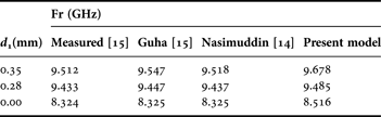
Change in the resonance frequency of a TMA with perfect conductor patch, caused by variation in air gap thickness was theoretically studied in [Reference Esselle and Verma14, Reference Guha and Siddiqui15]. The results of these studies are compared with our theory in Table 1. The comparison among the theories and measurements shows good agreement.
Table 1. Comparison of calculated resonant frequencies of equilateral triangular microstrip patch (W = 15.5 mm, d 2 = 0.508 mm, ɛ r2 = 2.2, ɛ r1 = 1).
The tunability has been theoretically studied in Fig. 9. The design data are presented for three different substrates having widely varying dielectric constant. The superconducting patch is fabricated with a YBCO thin film. The resonant frequency normalized with respect to that with d 1 = 0 is plotted against (d 1/d 2) with d 2 = 0.508 mm. In Fig. 9(a), the resonant frequency versus air separation (d 1/d 2) for various substrate materials is shown. It is observed that when the air separation grows, the resonant frequency increases rapidly until achieving a maximum operating frequency at a definite air separation d max. Note that the effect of the air gap is more pronounced for small values of d 1. This air gap tuning effect increases when the substrate relative permittivity value is increased. Graphical representation of the bandwidth is shown in Fig. 9(a). Note that it increases monotonically with increasing air separation.

Fig. 9. (a) Resonant frequency normalized. (b) Bandwidth normalized versus d1/d2 of HTSTMA structure (σ n = 106 S/m, λ0 = 140 nm and T c = 89 K, T = 50 K, d 2 = 0.508 mm, t = 350 nm, and W = 1.0 cm). (ɛ r2 = 13, FR0 = 5.097 GHz); (ɛr2= 9.6, FR0 = 5.82 GHz); (ɛ r2 = 6.6, FR0 = 6.87 GHz).
D) Radiations patterns of HTS equilateral triangular microstrip single layer antenna
Figure 10 shows the calculated radiation patterns (electric field components, E θ, E φ), of the HTS equilateral triangular patch printed on substrate thickness (d 2 = 254 µm). The mode excited is TM10. It is seen that the strongest radiation occurs in the broadside direction (θ = 0).

Fig. 10. Normalized radiation pattern (dB) of HTSTMA structure (σ n = 106 S/m, λ 0 = 140 nm and T/T c = 0.5, d 2 = 254 µm, t = 350 nm, ɛ r2 = 23.81, and W = 1.4 mm). (––––)E θ (ϕ = 0°); (– – –) E ϕ (ϕ = 90°).
E) Efficiency of HTSTMA structure
The efficiencies of the YBCO and copper triangular microstrip patch antennas are shown in Fig. 11. It is observed that there is a maximum improvement of 7.35% at 4.5 GHz in the efficiency of the HTSTMA structure when compared to the copper antenna at the same temperature. The benefits of using high temperature superconductors in microstrip antennas can be quite substantial owing to the reduced losses, which translates to an increase in the efficiency of the antenna [Reference Silva and D'assuncao23–Reference EL-Ghazaly, Hammond and Itoh25].

Fig. 11. HTSTMA structure efficiency (σ n = 106 S/m, λ 0 = 140 nm, T/T c = 0.5, ɛ r2 = 23.81, t gδ = 7.6 10−6, d 2 = 254 µm, t = 350 nm, W = 1.4 mm d 1= 0 mm, and σ C = 40 S/m).
IV. CONCLUSION
Theoretical results for resonant frequency and bandwidth have been presented for various ETMAs configurations. A spectral domain approach has been used for the numerical calculation. To include the effect of the superconductivity of the microstrip patch in spectral domain analysis, surface complex impedance has been considered. Numerical results for the effect of temperature and thickness of HTS thin film on resonant frequency and bandwidth have been presented. The properties of the HTSTMA structure were stable at temperatures slightly lower than the critical temperature. Also, computations show that the air separation can be adjusted to have the maximum operating frequency of the superconducting microstrip antenna. On the other hand, the bandwidth increases monotonically with increasing air gap width. The calculated results have been compared with the measured one available in the literature and good agreement has been found.
 O. Barkat was born in Constantine, Algeria in 1974. She received her Engineering Diploma in electronic engineering in 1999, as a Master in microwaves in 2002 and Ph.D. degrees in microwaves in 2009 from the Electronic Institute, University of Constantine. Currently, she is working as a Professor in the Department of Electronics Engineering. Her main field of interest is millimeter-wave antennas, active and passive circuits, antenna arrays, EBG structures, and their applications for microwave devices.


