


I. INTRODUCTION
Impact avalanche transit time (IMPATT) devices have already emerged as high power, high efficiency solid-state sources for both microwave (3–30 GHz) and millimeter-wave (mm-wave) (30–300 GHz) frequency bands [Reference Midford and Bernick1–Reference Gray, Kikushima, Morentc and Wagner3]. Several small-signal (S-S) analysis and simulation methodologies of IMPATT devices have already provided a considerable insight into the IMPATT operation [Reference Miswa4–Reference Gummel and Scharfetter6]. Several authors [Reference Roy, Sridharan, Ghosh, Pal and Miller7–Reference Acharyya and Banerjee12] investigated the mm-wave performance of double-drift region (DDR) Si IMPATT devices operating at different mm-wave atmospheric window frequencies following an S-S simulation technique based on Gummel–Blue approach [Reference Gummel and Blue13]. However, several important properties of IMPATT oscillators such as dependence of RF power output, DC to RF conversion efficiency, and frequency tuning of the oscillators on diode parameters, bias current, and RF circuitry cannot be precisely obtained from S-S analysis. Thus, large-signal (L-S) analysis of IMPATT devices is necessary to acquire the above-mentioned properties. Evans and Haddad [Reference Evans and Haddad14] presented an L-S model of IMPATT oscillator and RF power output, efficiency of the oscillator was obtained from a closed-form solution of nonlinear equations describing a Read-type (p–n–υ–n) IMPATT device in 1968. They assumed much shorter transit time of the charge carriers through the drift region as compared to the period of RF oscillation to obtain the closed-form solution. Pioneering work on L-S analysis of Read-type silicon IMPATT oscillator is carried out by Scharfetter and Gummel [Reference Scharfetter and Gummel15]. They obtained a self-consistent numerical solution for equations describing carrier transport, carrier generation, and space-charge balance and presented the theoretical calculations of L-S admittance and efficiency achievable in a silicon Read-type IMPATT diode. Gupta and Lomax [Reference Gupta and Lomax16] followed a current-excited L-S analysis along with circuit implementation in 1973. They assumed a sinusoidal current flowing through the device and obtained corresponding voltage response to calculate device impedance.
In the present paper, the authors have made an attempt to obtain the upper cut-off frequency limit of DDR Si IMPATTs through an avalanche response time based simulation approach [Reference Acharyya and Banerjee17–Reference Acharyya and Banerjee20]. An L-S simulation technique based on non-sinusoidal voltage excitation (NSVE) model [Reference Acharyya, Banerjee and Banerjee21–Reference Acharyya, Banerjee and Banerjee23] is developed and simulation is carried out to study L-S characteristics of DDR IMPATTs based on Si designed to operate at different mm-wave and terahertz (THz) frequencies up to the limiting frequency of IMPATT operation for DDR Si IMPATTs obtained from avalanche response time based simulation, i.e. up to 0.5 THz. The effect of parasitic series resistance on L-S properties of DDR Si IMPATTs is also investigated, which shows that the decrease in RF power output and conversion efficiency of the device due to series resistance is more prominent at higher frequencies. The NSVE L-S simulation results are compared with well-established double-iterative field maximum (DEFM) S-S simulation results and finally both are compared with the experimental results to cross check the validity of the proposed method.
II. L-S SIMULATION TECHNIQUE
One-dimensional model of a reverse biased n +–n–p–p + structure shown in Fig. 1 is used for the L-S simulation of DDR IMPATT device because of the physical phenomena taking place in the semiconductor bulk along the symmetry axis of the mesa structure of IMPATT devices. The fundamental time- and space-dependent device equations, such as Poisson's equation (equation (1)), continuity equations (equations (2) and (3)) and current density equations (equations (4) and (5)) involving mobile space charge in depletion layer are simultaneously solved under L-S conditions with appropriate boundary conditions by using a DEFM simulation method [Reference Acharyya, Banerjee and Banerjee21–Reference Acharyya, Banerjee and Banerjee23]. The fundamental device equations are given by
 $$\displaystyle{{d\xi \lpar x\comma t\rpar } \over {dx}}=\displaystyle{q \over {\varepsilon _s }}\lpar N_D - N_A+p\lpar x\comma t\rpar - n\lpar x\comma t\rpar \rpar \comma \; $$
 $$q\displaystyle{{\partial p\lpar x\comma t\rpar } \over {\partial t}}=- \displaystyle{{\partial J_p \lpar x\comma t\rpar } \over {\partial x}}+\lpar \alpha _n \lpar x\comma t\rpar J_n \lpar x\comma t\rpar +\alpha _p \lpar x\comma t\rpar J_p \lpar x\comma t\rpar \rpar \comma \; $$
 $$q\displaystyle{{\partial n\lpar x\comma t\rpar } \over {\partial t}}=\displaystyle{{\partial J_n \lpar x\comma t\rpar } \over {\partial x}}+\lpar \alpha _n \lpar x\comma t\rpar J_n \lpar x\comma t\rpar +\alpha _p \lpar x\comma t\rpar J_p \lpar x\comma t\rpar \rpar \comma \; $$
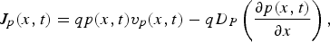 $$J_p \lpar x\comma t\rpar =qp\lpar x\comma t\rpar v_p \lpar x\comma t\rpar - qD_P \left({\displaystyle{{\partial p\lpar x\comma t\rpar } \over {\partial x}}} \right)\comma \; $$
 $$J_n \lpar x\comma t\rpar =qn\lpar x\comma t\rpar v_n \lpar x\comma t\rpar +qD_n \left({\displaystyle{{\partial n\lpar x\comma t\rpar } \over {\partial x}}} \right)\comma \; $$
Fig. 1. One-dimensional model of DDR IMPATT device.
where N D and N A are the donor and acceptor concentrations, αn(x,t) and αp(x,t) are the electron and hole ionization rates at the space point x at the instant t, v n(x,t) and v p(x,t) are the electron and hole drift velocities at x at the instant t, D n and D p are the electron and hole diffusion coefficients, p(x,t) and n(x,t) are respectively the electron and hole concentrations at x at the instant t, ξ(x,t) is the electric field at x at the instant t, J n(x,t) and J p(x,t) are respectively the electron and hole components of bias current density (J 0(t) = J n(x,t) + J p(x,t)) at x at the instant t, q is the electric charge of an electron (q = 1.6 × 10⁻¹⁹ C), and ɛ s is the permittivity of the semiconductor material. Boundary conditions are imposed at the contacts (i.e. n +–n and p +–p interfaces) by setting up appropriate restrictions in equations (1)–(5). The boundary conditions for the time varying electric field at depletion layer edges are given by [Reference Acharyya, Banerjee and Banerjee21–Reference Acharyya, Banerjee and Banerjee23]
 $$\xi \lpar {-} x_1\comma t\rpar =0\quad \; {\rm and}\quad \xi \lpar {+}x_2\comma t\rpar = 0.$$
Similarly, the boundary conditions for time varying normalized current density P(x,t) = (J p(x,t) − J n(x,t))/J 0(t) at depletion layer edges, i.e. at x = −x 1 and x = x 2 are given by [Reference Acharyya, Banerjee and Banerjee21–Reference Acharyya, Banerjee and Banerjee23]
 $$\eqalign{&P\left({ - x_1\comma t} \right)=\left({\displaystyle{2 \over {M_p \lpar {-} x_1\comma t\rpar }} - 1} \right)\; \quad {\rm and}\cr& P\left({+x_2\comma t} \right)=\left({1 - \displaystyle{2 \over {M_n \lpar {+}x_2\comma t\rpar }}} \right)\comma \; }$$
where M n(x 2,t) and M p(−x 1,t) are the electron and hole multiplication factors at depletion layer edges at instant t are given by
 $$\eqalign{&M_p \left({ - x_1\comma t} \right)=\displaystyle{{J_0 \lpar t\rpar } \over {J_p \lpar - x_1\comma t\rpar }}\quad \; {\rm and }\cr& M_n \left({+x_2\comma t} \right)=\displaystyle{{J_0 \lpar t\rpar } \over {J_n \lpar +x_2\comma t\rpar }}.}$$
The total diode voltage (V B(t)) and avalanche zone voltage drop (V A(t)) at a particular instant of time t are obtained from numerical integration of the field profile over the depletion layer and avalanche layer widths respectively as follows:
 $$V_B \left(t \right)=\vint_{ - x_1 }^{x_2 } {\xi \left({x\comma t} \right)dx} \; \quad {\rm and}\quad V_A \left(t \right)=\vint_{ - x_{A1} }^{x_{A2} } {\xi \left({x\comma t} \right)dx} .$$
DC values of peak electric field (ξp), breakdown voltage (V B), and avalanche zone voltage (V A) drop can be evaluated by taking the time averages of time varying peak electric field (ξp(t)), total diode voltage (V B(t)), and avalanche zone voltage drop (V A(t)) over a complete time period of steady-state oscillation (T = 1/f; where f is the fundamental frequency of steady-state oscillation). Thus, the DC values of the peak electric field (ξp), breakdown voltage (V B), and avalanche zone voltage (V A) are given by
 $$\eqalign{&\xi _p=\displaystyle{1 \over T}\vint_0^T {\xi _p \left(t \right)dt}\comma \; \quad V_B=\displaystyle{1 \over T}\vint_0^T {V_B \left(t \right)dt} \quad {\rm and}\cr& V_A=\displaystyle{1 \over T}\vint_0^T {V_A \left(t \right)dt} .}$$
The L-S simulation is carried out by considering the IMPATT device as a non-sinusoidal voltage driven source, shown in Fig. 2. The input AC voltage is given as
 $$V_{RF} \left(t \right)=V_B \sum\limits_{p=1}^n {m_x ^p } \sin \left({p\omega t} \right).$$
Fig. 2. Voltage driven IMPATT diode oscillator and associated circuit.
The bias voltage is applied across the device through a coupling capacitor (C) to study the performance of the device at a given fundamental frequency (f = ω/2π) with its n harmonics. The snapshots of electric field and current density profiles in the depletion layer of the IMPATT device are obtained from simultaneous numerical solutions of the basic device equations (equations (1)–(5)) subject to appropriate boundary conditions (equations (6) and (7)). The L-S simulation is carried out by taking 500 space steps and 100–150 time steps with sufficient accuracy.
The L-S program is run until the limit of one complete cycle (i.e. 0 ≤ ωt ≤ 2π) is reached. A current source provides the necessary bias current density. The RF voltage amplitude is V RF and operating frequency is f. The waveforms associated with terminal current and voltage during a complete cycle of oscillation are Fourier analyzed to study the high-frequency characteristics of the device at various instants of time (ωt = 0, π/2, π, 3π/2, and 2π). The simulation is repeated at consecutive cycles to confirm the stability of oscillation. The simulated values of L-S negative conductance (G(ω)), susceptance (B(ω)), negative resistance (Z R(ω)), reactance (Z X(ω)), and Q-factor (Q p = −B p/G p), where G p and B p are L-S peak negative conductance and susceptance at optimum frequency (f p)) respectively are obtained from this study. The L-S values of negative conductance (G(ω)) and susceptance (B(ω)) (both are normalized by device junction area A 0: considering circular cross-sectional area of the device, A 0 = π(D 0/2)2; where D 0 is the device effective junction diameter) are their effective values at the fundamental frequency of the voltage source, obtained by detailed Fourier analysis of the terminal current and voltage waveforms. The L-S device admittance is Y D(ω) = [G(ω) + jB(ω)]A 0. The L-S device impedance is given by
 $$Z_D \left(\omega \right)=\displaystyle{1 \over {Y_D \lpar \omega \rpar }}=\displaystyle{1 \over {\lsqb G\lpar \omega \rpar +jB\lpar \omega \rpar \rsqb A_0 }}=Z_R \left(\omega \right)+jZ_X \left(\omega \right).$$
The L-S negative resistance (Z R(ω)) and reactance (Z X(ω)) of the device are given by
 $$\eqalign{&Z_R \left(\omega \right)=\displaystyle{{G\lpar \omega \rpar } \over {\lsqb G\lpar \omega \rpar ^2+B\lpar \omega \rpar ^2 \rsqb A_0 }}\; \quad {\rm and}\cr& Z_X \left(\omega \right)=\displaystyle{{ - B\lpar \omega \rpar } \over {\lsqb G\lpar \omega \rpar ^2+B\lpar \omega \rpar ^2 \rsqb A_0 }}.}$$
If R S is the series resistance associated with the device then the effective device impedance is modified to
 $$Z_{D_{eff} } \left(\omega \right)=\left({Z_R \left(\omega \right)+R_S } \right)+jZ_X \left(\omega \right).$$
The effective admittance of the device is now modified to
 $$Y_{D_{eff} } \left(\omega \right)=\displaystyle{1 \over {Z_{D_{eff} } \left(\omega \right)}}=\left[{G_{eff} \left(\omega \right)+jB_{eff} \left(\omega \right)} \right]A_0 .$$
Now, the effective L-S RF power output (P RF) may be calculated as
 $$P_{RF}=\displaystyle{1 \over 2}V_{RF} ^2 \left\vert {\left({G_{eff} } \right)_p } \right\vert A_0\comma \; $$
where V RF is the RF voltage, |(G eff)p| is the magnitude of L-S peak effective negative conductance normalized with respect to effective junction area (A 0). The effective L-S DC to RF conversion efficiency (ηL) of the device is obtained from the equation
 $$\eta _L=\displaystyle{{P_{RF} } \over {P_{DC} }}\comma \; $$
where P DC = J 0V BA 0 is the input DC power and J 0 is the bias current density.
III. CALCULATION OF AVALANCHE RESPONSE TIME
The avalanche response time of DDR IMPATTs can be calculated from the knowledge of static spatial distribution of electron and hole ionization rates (α n(x) versus x and α p(x) versus x) obtained from DC simulation, saturated drift velocities of charge carriers (v sn and v sp). If τ An and τ Ap are avalanche response times initiated by electrons and holes, respectively, then these are expressed as [Reference Acharyya and Banerjee17–Reference Acharyya and Banerjee20]
 $$\tau _{An}=\displaystyle{1 \over {\lpar v_{sn}+v_{sp} \rpar }}\vint_{ - x_{A1} }^{x_{A2} } {\exp \left[{ - \vint_{ - x_{A1} }^x {\left({\alpha _n \left(x \right)- \alpha _p \left(x \right)} \right)dx^{\prime}} } \right]} dx\comma \; $$
 $$\tau _{Ap}=\tau _{An} \exp \left[{\vint_{ - x_{A1} }^{x_{A2} } {\left({\alpha _n \left(x \right)- \alpha _p \left(x \right)} \right)dx} } \right].$$
When avalanche process is initiated by a mixture of electrons and holes then the corresponding response time τ A is given by [Reference Acharyya and Banerjee17–Reference Acharyya and Banerjee20]
 $$\tau _A=\tau _{An} \left\{{\left({1 - k} \right)+k \cdot \exp \left[{ - \vint_{ - x_{A1} }^{x_{A2} } {\left({\alpha _n \left(x \right)- \alpha _p \left(x \right)} \right)dx} } \right]} \right\}^{ - 1}\comma \; $$
where the parameter k = J ps /J s and (1 − k) = J ns /J s; J s = J ps + J ns is the total reverse saturation current of the device under dark condition. The expressions for thermally generated electron and hole reverse saturation currents (J ns, J ps) are given by
 $$J_{ns}=\left({\displaystyle{{qD_n n_i ^2 } \over {L_n N_A }}} \right)\quad \; {\rm and}\quad J_{ps}=\left({\displaystyle{{qD_p n_i ^2 } \over {L_p N_D }}} \right)\comma \; $$
where D n and D p are the diffusion coefficients of electrons and holes, respectively, L n and L p are the diffusion lengths of electrons and holes, respectively, n i is the intrinsic carrier concentration, N D and N A are the donor and acceptor concentrations, respectively. Static spatial distribution of electron and hole ionization rates (α n(x) and α p(x)) are obtained from the static or DC simulation of DDR IMPATTs. DC simulation is conducted by solving the basic device equations (equations (1)–(5)) simultaneously subject to proper boundary conditions (equations (6) and (7)) in static mode (time independent), i.e. by keeping the voltage modulation factor, m x = 0.
IV. RESULTS AND DISCUSSION
A) Design of structural, doping, and other parameters
The active layer widths (W n, W p) and background doping concentrations (N D, N A) of DDR IMPATTs based on Si are initially chosen by using the transit time formula of Sze and Ryder [Reference Sze and Ryder24]. The structural and doping parameters of the devices are designed for optimum performance at different mm-wave and THz frequencies (i.e. at design frequency, f d) by using the method described in earlier papers [Reference Acharyya, Banerjee and Banerjee21–Reference Acharyya, Banerjee and Banerjee23]. The doping concentrations of n +- and p +-layers (N n+ and N p+) are taken much higher, in the order of ~1025/m3 in the simulation. Structural and doping parameters of the designed Si-based DDR IMPATT devices are given in Table 1. The realistic field dependence of ionization rates (α n, α p) and drift velocities (v n, v p) of charge carriers and other material parameters such as bandgap (E g), intrinsic carrier concentration (n i), effective density of states of conduction and valance bands (N c, N v), diffusion coefficients (D n, D p), mobilities (μ n, μ p), and diffusion lengths (L n, L p) of Si (at realistic junction temperature of 500 K) are taken from the recently published experimental reports [Reference Grant25–28].
Table 1. Structural and doping parameters.

B) Static characteristics
Important static or DC parameters such as peak electric field (ξp), breakdown voltage (V B), avalanche zone voltage (V A), ratio of drift zone voltage drop to breakdown voltage (V D/V B), avalanche layer width (x A), and ratio of avalanche zone width to total depletion layer width (x A/W) of the designed DDR Si IMPATTs are obtained from the static simulation as mentioned earlier and are given in Table 2. Variations of ξp, V B, and V A with operating frequency of Si-based DDR IMPATTs are shown in Fig. 3. Table 2 shows that peak electric field (ξp) increases, while the breakdown voltage (V B), avalanche zone voltage (V A), and avalanche layer width (x A) decrease in DDR IMPATTs based as the operating frequency increases. Peak electric field (ξp) increases from 6.03700 × 10⁷–12.3120 × 10⁷ V/m in Si IMPATTs as the operating frequency increases from 94 GHz to 0.5 THz. From the knowledge of avalanche zone voltage (V A) and breakdown voltage (V B), the drift zone voltage (V D = V B − V A) of the device can be calculated. The ratio of drift zone voltage to breakdown voltage (V D/V B) decreases in the devices under consideration as the operating frequency increases. At higher frequencies the ratio V D/V B decreases sharply in Si DDRs (V D/V B = 0.3346 at 94 GHz; whereas V D/V B = 0.1615 at 0.5 THz). According to the semi-quantitative formula of DC to RF conversion efficiency (ηL = (1/π) × (V D/V B)) [Reference Scharfetter and Gummel15] the DC to RF conversion efficiency (ηL) of IMPATT devices is directly proportional to the ratio V D/V B. Thus, the DC to RF conversion efficiency of Si IMPATTs is expected to decrease sharply with the increase of operating frequency.

Fig. 3. Variations of breakdown voltage, avalanche voltage, and peak electric field with optimum frequency of DDR Si IMPATTs.
Table 2. Static parameters.

The ratio of avalanche zone width to total drift layer width (x A/W) in Si IMPATTs increases sharply at higher operating frequencies. Higher x A/W indicates wider avalanche zone, which leads to higher avalanche voltage (V A) and lower drift zone voltage (V D). Lower V D/V B, lower is the conversion efficiency. Thus, the rapid widening of the avalanche region at higher operating frequencies is the primary cause of sharp decrease of conversion efficiency at higher operating frequencies in Si IMPATTs. In the case of Si DDRs, x A/W is 44.62% at 94 GHz but it rises to 63.03% at 0.5 THz which causes sharp decrease of conversion efficiency at 0.5 THz frequency.
C) Thermal design
It is well known that the RF power output of IMPATT devices increases with the increase of junction temperature [Reference Midford and Bernick1, Reference Acharyya, Banerjee and Banerjee21]. Thus, the junction temperature of the device must be kept fixed well above the room temperature (T j > T 0 = 300 K) but below the burnout temperature (T B) of the base material (here, T B of the base material silicon is 575 K) by proper thermal design and appropriate heat sinking arrangement to avoid the thermal runway phenomenon and consequent device burnout. Generally, the junction temperatures of IMPATTs based on silicon are kept near 500 K for steady-state CW operation by using suitable heat sinks made of either metal (copper or silver) or type-IIA diamond [Reference Midford and Bernick1, Reference Acharyya, Mukherjee, Mukherjee and Banerjee29, Reference Acharyya, Pal and Banerjee30]. However, a significant thermal advantage can be obtained by using a type-IIA diamond as heat sink material [Reference Midford and Bernick1] due to its high thermal conductivity (k dm = 1200 W/m/K [28] at 500 K). A simple method of designing heat sink has been proposed by Acharyya et al. [Reference Acharyya, Mukherjee, Mukherjee and Banerjee29] in 2011, where they have modeled the heat transfer in ordinary mesa structured DDR IMPATT diode on semi-infinite heat sink by using a lumped analytical representation of heat flow in both upper and bottom sides of the p–n junction. They showed that heat transfer mainly occurred from the p–n junction through the bottom side of the n +–n–p–p + mesa structure (i.e. p-layer → p +-layer → metal contacts (Ti, Au) → heat sink) during CW steady-state operation due to much smaller thermal resistance of the bottom side as compared to that of the upper side. Thus, the total effective thermal resistance of the device on the semi-infinite heat sink (θ T) can be written as
 $$\theta _T=\left({\theta _p+\theta _{p^+}+\theta _{Ti}+\theta _{Au} } \right)+\theta _{HS}\comma \; $$
where θ p, θ p+, θ Ti, θ Au are the thermal resistances of p-, p +-layers of the device, Ti, Au contact layers respectively, and θ HS is the thermal resistance of the semi-infinite heal sink. The thermal resistance of p-epitaxial layer and Ti, Au contact layers can be written as
 $$\eqalign{&\theta _p=\left({\displaystyle{{4W_p } \over {\pi D_0 \,^2 k_{Si} }}} \right)\comma \; \quad \theta _{Ti}=\left({\displaystyle{{4W_{Ti} } \over {\pi D_{S - 1} \, ^2 k_{Ti} }}} \right)\quad \; {\rm and}\cr& \theta _{Au}=\left({\displaystyle{{4W_{Au} } \over {\pi D_{S - 1} \,^2 k_{Au} }}} \right)\comma \; }$$
respectively, where W p, W Ti, and W Au are the thicknesses of p-epitaxial layer and Ti, Au contact layers respectively, D 0 is the junction diameter, D S−1 is the diameter of the device–heat sink interface (diameters of Ti, Au contact layers) and k Si, k Ti, and k Au are the thermal conductivities of Si, Ti, and Au respectively (k Si = 150.00 W/m/K, k Ti = 21.90 W/m/K, k Au = 320.00 W/m/K [31]). The mesa etched p +-layer is considered to consist of a number of concentric cylindrical layers one below the other each having the same thickness (W p+/S; where S is the number of cylinders) with increasing diameter from D 0 to D S−1 as shown in Fig. 4. The expression of thermal resistance due to p +-layer can be written as
 $$\theta _{p+}=\left({\displaystyle{4 \over {\pi k_{Si} }}} \right)\sum\limits_{m=0}^{S - 1} {\left({\displaystyle{{W_{p+} } \over {SD_m ^2 }}} \right)} .$$
Fig. 4. Mesa structure of DDR IMPATT device on semi-infinite heat sink; the mesa etched p +-layer is considered to consist of a number of concentric cylindrical layers one below the other each having the same thickness (W p+/S; where S is the number of cylinders) with increasing diameter from D 0 to D S−1.
In the present calculation, the number of concentric cylindrical layers S is taken as 100 to achieve approximate tapered conical-shaped structure of p +-layer with sufficient accuracy which is near approximation of mesa etched p +-layer. Thickness of different layers (p-, p +-layers of the device, Ti, and Au contact layers) and device–heat sink interface diameters (D S−1) of DDR Si IMPATT operating at different mm-wave and THz frequencies are given in Table 3.
Table 3. Thickness of different layers and device–heat sink interface diameters.

The thermal resistance of the heat sink having thickness L H and diameter D H can be written as
 $$\theta _{HS}=\left({\displaystyle{{4L_H } \over {\pi D_{\!H}^{2}\, k_{dm} }}} \right)\comma \; $$
where k dm is the thermal conductivity of heat sink material (type-IIA diamond). The junction temperature of the device in CW steady-state operation can be obtained from the following relation:
 $$T_j=T_0+\left({\displaystyle{\pi \over 4}} \right)\left({1 - \eta _L } \right)J_0 V_B D_0 \,^2 \theta _T $$
where T 0 is the ambient temperature (T 0 = 300 K). The values of V B and J 0 are obtained from the DC simulation of DDR Si IMPATT device designed to operate at a particular frequency. The DC to RF conversion efficiency (η L) of the device at that frequency is initially estimated from the NSVE L-S simulation presented in this paper (later in this paper). Now, if θ T is known, then the junction temperature can be calculated from equation (26). However, in the present problem, T j has to be kept near 500 K to get maximum RF power from the device avoiding the device burnout. Thus, the device junction diameter (D 0) and heat sink dimensions (L H and D H) have to be chosen appropriately keeping all other dimensions of the device fixed such that T j remains nearly 500 K.
The flowchart of the method of obtaining D 0, L H, and D H is shown in Fig. 5. At first, the junction temperature (T j) of the device design to operate at a particular frequency (f d) is calculated from equation (26) by using the corresponding bias current density (J 0), breakdown voltage (V B) obtained from DC simulation, initially estimated DC to RF conversion efficiency (η L) from the NSVE L-S simulation, initially chosen junction diameter (D 0), and heat sink dimensions (L H and D H; where D H ≫ D 0, otherwise device-heat sink bonding is difficult to achieve). If the calculated T j remains within the range of 480–520 K, then the D 0, L H, and D H values are accepted provided that D H ≫ D 0, otherwise D 0, L H, and D H values are modified accordingly (keeping D H ≫ D 0) and again T j is calculated from equation (26). The process is repeated until appropriated D 0, L H, and D H values are obtained for which 480 ≤ T j ≤520. The finally estimated D 0, L H, and D H values, corresponding thermal resistance of the device (θ D = θ p + θ p+ + θ Ti + θ Au), and total effective thermal resistance of the device on semi-infinite heat sinks (θ T = θ D + θ HS) designed to operate at different mm-wave and THz frequencies and corresponding junction temperatures (T j) are given in Table 4.

Fig. 5. Flowchart showing the method of obtaining D 0, L H, and D H.
Table 4. Junction diameters, heat sink dimensions, thermal resistances, and junction temperatures of DDR Si IMPATTs designed to operate at different mm-wave and THz frequencies.

D) Avalanche response times
Avalanche response times (τ A) of DDR IMPATTs based on Si are calculated by equation (20). Spatial variations of ionization rates of electrons (α n) and holes (α p) for each device are obtained from the output of the static program and used to solve equations (18) and (20). Transit times (τ T) associated with the DDR IMPATT devices based on Si operating at different mm-wave and THz frequencies are obtained from transit time formula of Sze and Ryder [Reference Sze and Ryder24]. Figure 6 shows the variations of τ A and τ T with operating frequency in Si-based DDRs. DDR IMPATTs based on a particular semiconductor can be operated at higher frequencies provided the avalanche response time (τ A) is much lower than the transit time (τ T) of carriers at the higher frequencies [Reference Acharyya and Banerjee17–Reference Acharyya and Banerjee20]. Avalanche response time (τ A) of the device depends on saturated drift velocities and ionization rates of electron and holes (v sn, v sp and α n, α p, respectively) of the base semiconductor. Thus, the type of the base material determines the value of τ A at a particular frequency. Figure 6 shows that the avalanche response time (τ A) of Si DDRs becomes almost comparable to transit time (τ T) as the operating frequency increases to 0.5 THz, which implies that above 0.5 THz, it is difficult to achieve IMPATT action in Si-based DDR IMPATTs. Thus, the highest operating frequency of Si DDRs is limited to 0.5 THz.

Fig. 6. Variations of avalanche response time and transit time with optimum frequency of DDR Si IMPATTs.
E) L-S characteristics
The important L-S parameters of Si-based DDR IMPATTs designed to operate at different mm-wave and THz frequencies such as peak optimum frequency (f p), avalanche resonance frequency (f a), peak negative conductance (G p), corresponding susceptance (B p), quality factor or Q-factor (Q p = −B p/G p), negative resistance (Z R), RF power output (P RF), and L-S DC to RF conversion efficiency (η L) for 50% voltage modulation are obtained from the L-S simulation assuming series resistance, R S = 0 and those are listed in Table 5. The voltage modulation factor is taken as 50%, since it was earlier studied that the 94 GHz DDR Si IMPATT delivers maximum RF power when the voltage modulation factor is kept in the range of 50–60% [Reference Acharyya, Banerjee and Banerjee21–Reference Acharyya, Banerjee and Banerjee23]; which is also verified and confirmed for DDR Si IMPATTs operating at higher frequencies in the present study. Admittance characteristics or conductance–susceptance plots for 94, 140, 220, and 300 GHz Si DDR IMPATTs for 50% voltage modulation are shown in Fig. 7 while the same plots for 0.5 THz Si IMPATT are shown in Fig. 8. It is observed from Table 5, Figs 7, and 8 that the magnitudes of G p and B p increase with the increase of operating frequency in those devices. Avalanche resonance frequency (f a) of the IMPATT device is the frequency at which the conductance of the device changes its sign from positive to negative. It can be observed from Table 5 that f a increases sharply from 52.0 GHz to 196.7 GHz as the operating frequency increases from 94 GHz to 0.5 THz. Q-factor (Q p = −B p/G p) of the device determines the growth rate of IMPATT oscillation. Lower Q-factor closer to one (i.e. Q p ≈ 1) suggests a higher oscillation growth rate. It is observed from Table 5 that the Q-factor of Si-based DDR IMPATTs increases from 4.17 to 11.62 as the operating frequency increases from 94 GHz to 0.5 THz. Thus, the oscillation growth rate degrades as the frequency of operation increases. It is also worth noting from Table 5 that the magnitude of negative resistance (Z R) of Si IMPATTs decreases sharply with the operating frequency, which is the primary cause of sharp decrement of RF power output at higher operating frequencies.

Fig. 7. Admittance characteristics of 94, 140, 220, and 300 GHz DDR Si IMPATTs.

Fig. 8. Admittance characteristics of 0.5 THz DDR Si IMPATT.
Table 5. L-S parameters (R S = 0).

F) Effect of parasitic series resistance
In an IMPATT oscillator the RF power should be efficiently transferred from the active region of the device to the external load. This can be ensured by matching the real part of device impedance to the real part of load impedance by using a matching network with low loss at the resonant frequency at which total reactance of the device–circuit combination is zero [Reference Kurokawa32]. However, the power loss taking place in the inactive region of the device cannot be compensated for by the external circuitry. This loss should be minimized; otherwise it can severely degrade overall performance of the oscillator. The undepleted portion of the device contributes to positive series resistance and RF power is dissipated there as heat. The parasitic series resistance originates from the un-swept epitaxial layer, substrate layer, and contact layers of the device. Since the negative resistance of mm-wave IMPATTs is in the range of a few ohms, positive series resistance is to be kept to a minimum possible value by appropriate design of the structural, doping, and bias current parameters of the device to obtain maximum RF power output from the device.
The RF power out, DC to RF conversion efficiency, and junction temperature of DDR Si IMPATTs designed to operate at 94, 140, 220, 300, and 500 GHz are calculated for different values of series resistance (R S) and given in Table 6. It is interesting to observe from Table 6 that both the RF power output and conversion efficiency of the device operating at a particular frequency decreases with the increase of the value of series resistance. The effective magnitude of the device negative resistance (i.e. |Z R + R S|; where the sign of Z R is negative) decreases as R S increases; consequently, the RF power output and hence the conversion efficiency decreases. Owing to reduction in DC to RF conversion efficiency (η L) as a consequence of increase in R S, more power is dissipated as heat (P DISP = (1 − η L) × P DC) within the device, which leads to increase in junction temperature of the device. The percentages of decrease in RF power output due to parasitic series resistance (i.e. |ΔP RF|/P RF0 (%); where ΔP RF = |(P RF − P RF0)|, P RF is the RF power output of the device for R S > 0 and P RF0 is the RF power output of the device when R S = 0) of DDR Si IMPATTs at different operating frequencies are shown as bar graphs in Fig. 9. It is worth noting from Table 6 and Fig. 9 that, the effect of series resistance is more prominent in devices operating at higher frequencies, especially in the device operating at the THz regime (i.e. 0.3 and 0.5 THz). This is mainly due to the magnitude of negative resistance (Z R) of the device which is very small at higher frequency (THz) devices as shown in Table 5. Thus, at higher frequencies, the value of series resistance must be kept very small to get RF power output from those devices, otherwise real part of equation (14) may no longer remain negative, causing no RF power output from the device.

Fig. 9. Bar graphs representing the percentages of decrease in RF power output of DDR Si IMPATTs due to parasitic series resistance.
Table 6. RF power outputs, DC to RF conversion efficiencies, and junction temperatures for different values of R S.

G) Validation of the simulation results
Figure 10 shows the variations of RF power output of DDR Si IMPATTs obtained from NSVE L-S simulation presented in this paper for different R S values, well-established DEFM S-S simulation for R S = 0 [Reference Acharyya and Banerjee17] and experimental measurements [Reference Midford and Bernick1, Reference Luy, Casel, Behr and Kasper33, Reference Wollitzer, Buchler, Schafflr and Luy34] with optimum frequency. Luy et al. [Reference Luy, Casel, Behr and Kasper33], fabricated DDR IMPATTs based on Si designed to operate at 94 GHz. They obtained peak RF power of 600 mW at 94 GHz with 6.7% DC to RF conversion efficiency from their molecular beam epitaxy (MBE) grown p +–p–n–n + structured IMPATT diode. The NSVE L-S simulation of DDR Si IMPATT device at 94 GHz shows the device is capable of delivering 657.54 mW peak RF power output with 8.25% conversion efficiency for a hypothetically assumed 0.0 Ω series resistance at a voltage modulation of 50%. The RF power and efficiency reduced to 640.15 mW and 8.03%, respectively, for the same voltage modulation if the series resistance of the device is 0.2 Ω, which is the experimentally obtained series resistance of 94 GHz DDR Si IMPATT under practical operating conditions [Reference Luy, Casel, Behr and Kasper33]. However, DEFM S-S simulation predicts that the same device can deliver 708.43 mW of peak RF power with 10.58% conversion efficiency at 94 GHz for 30% voltage modulation [Reference Acharyya and Banerjee17]. The deviation of NSVE L-S and DEFM S-S simulation results with respect to experimental results are 6.7–9.6% and 18.1%, respectively, in terms of RF power output and 19.9–23.1% and 57.9% in terms of DC to RF conversion efficiency. Wollitzer et al. [Reference Wollitzer, Buchler, Schafflr and Luy34], obtained 225 mW peak RF power output from a 140 GHz DDR Si IMPATT oscillator, while the RF power outputs of DDR Si IMPATTs obtained from NSVE L-S and DEFM S-S simulations at 140 GHz are 334.49 and 446 mW, respectively. Thus, it is clear from the above comparison that the NSVE L-S simulation results are in closer agreement with the experimental results as compared to those of DEFM S-S simulation results. This fact can be explained a follows. Practically, IMPATT diodes operate in L-S mode, where voltage modulation remains within 50–60%. DEFM S-S simulation which is valid for up to 30% voltage modulation due to the S-S approach is not sufficient to predict RF power output and efficiency of the device accurately and the practical situation demands L-S simulation. Midford and Bernick [Reference Midford and Bernick1], obtained 50 mW RF power output from 220 GHz, DDR Si IMPATT diode. However, NSVE L-S and DEFM S-S simulation predicts that the device can deliver 297.20 and 334.23 mW of peak RF power, respectively, at 220 mW. This discrepancy between the simulated and experimental results at 220 GHz may be due to the un-optimized device structure, different biasing conditions, inappropriate experimental arrangements, etc. adopted by the experimentalists in [Reference Midford and Bernick1]. However, NSVE L-S simulation is expected to predict more accurate RF power output as compared to DEFM S-S simulation. As far as authors knowledge is concerned, no experimental report is available in the published literature till date on DDR Si IMPATTs operating at THz frequencies (0.3 and 0.5 THz). Thus, the simulation results of 0.3 and 0.5 THz DDR Si IMPATTs could not be compared with the experimental results. However, better prediction of RF power output from DDR Si IMPATTs at 94, 140, and 220 GHz by NSVE L-S simulation which is closer to the experimental results as compared to conventional DEFM S-S simulation, provides much greater assurance in the proposed approach even at the THz regime.
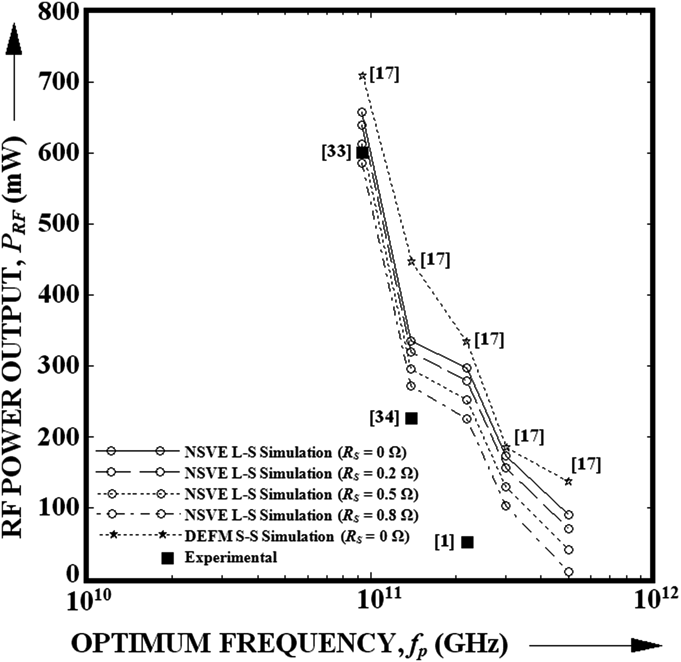
Fig. 10. Variations of RF power output with optimum frequency of DDR Si IMPATTs.
V. CONCLUSION
The L-S characterization of DDR IMPATT devices based on Si designed to operate at different mm-wave and THz frequencies up to 0.5 THz is carried out in this paper. The upper cut-off frequency limit of DDR Si IMPATTs is obtained as 0.5 THz from the avalanche response time based study. The effect of parasitic series resistance on the L-S properties of DDR Si IMPATTs is also investigated, which shows that the decrease in RF power output and conversion efficiency of the device due to series resistance is more pronounced at higher frequencies especially at the THz regime. The NSVE L-S simulation results are compared with well established DEFM S-S simulation results and finally both are compared with the experimental results. The comparative study shows that the proposed NSVE L-S simulation results are in closer agreement with experimental results as compared to those of DEFM S-S simulation. The present study strongly validates the NSVE L-S simulation scheme developed by the authors and simulation study explores the potentiality of DDR Si IMPATTs as powerful terahertz solid-state sources. The design considerations and L-S results presented in this paper will be worthwhile for future experimentalists and encourage them to fabricate DDR Si IMPATTs operating at the THz regime for several possible THz applications such as THz imaging, spectroscopy, bio-sensing, quality inspection in various industrial branches, medical and pharmaceutical applications, THz astronomy, etc.
 Aritra Acharyya received his M.Tech. degree in Radio Physics and Electronics from Institute of Radio Physics and Electronics, University of Calcutta, Kolkata, W.B., India. Earlier he had obtained his B.E. degree in Electronics and Telecommunication Engineering from Bengal Engineering and Science University, Shibpur, Howrah, W.B., India. Presently, he is pursuing his Ph.D. from University of Calcutta under Professor (Dr.) J.P. Banerjee, Radio Physics and Electronics Department, University of Calcutta, Kolkata, India. He joined the Department of Electronics and Communication Engineering, Supreme Knowledge Foundation Group of Institutions, Sir J.C. Bose School of Engineering, Mankundu, Hooghly, W. B., India in 2010 as a lecturer. He has been working as an Assistant Professor in the same institution since 2011. He is also working as a guest faculty for Biomedical Instrumentation Department of University of Calcutta, India. He is the recipient of Pareshlal Dhar Bhowmik book award for the year 2010 for securing highest marks in M.Tech. (Radio Physics and Electronics) Examination 2010 of the University of Calcutta. His research interest is millimeter-wave and terahertz semiconductor devices and their optical control. He is the principle co-author of more than 50 research papers in different national and international journals and conference proceedings.
 Jit Chakraborty was born in 1991. He is pursuing B.Tech. Course in Electronics and Communication Engineering from Supreme Knowledge Foundation Group of Institutions, Sir J.C. Bose School of Engineering, Mankundu, Hooghly, W.B., India. His area of interest is millimeter-wave and terahertz sources.
 Kausik Das was born in 1989. He is pursuing B.Tech. Course in Electronics and Communication Engineering from Supreme Knowledge Foundation Group of Institutions, Sir J.C. Bose School of Engineering, Mankundu, Hooghly, W.B., India. His area of interest is millimeter-wave and terahertz sources.
 Subir Datta was born in 1991. He is pursuing B.Tech. Course in Electronics and Communication Engineering from Supreme Knowledge Foundation Group of Institutions, Sir J.C. Bose School of Engineering, Mankundu, Hooghly, W.B., India. His area of interest is millimeter-wave and terahertz sources.
 Pritam De was born in 1990. He is pursuing B.Tech. Course in Electronics and Communication Engineering from Supreme Knowledge Foundation Group of Institutions, Sir J.C. Bose School of Engineering, Mankundu, Hooghly, W.B., India. His area of interest is wide-bandgap semiconductor based millimeter-wave and terahertz sources.
 Suranjana Banerjee received her B.Tech and M.Tech. degrees from the Institute of Radio Physics and Electronics, University of Calcutta, Kolkata, W.B., India. She topped the list of Electronics Honours graduates of Calcutta University in 2002. Presently, she is working as an Assistant Professor for Electronics and Communication Engineering Department in Academy of Technology, West Bengal University of Technology, Adisaptagram, Hooghly 712121, West Bengal, India. She has been carrying out research for Ph.D. degree in the area of millimeter wave hetero-junction ATT devices. She is the co-author of several research papers published in the proceedings of international conferences and refereed journals.
 Professor (Dr.) Jyotiprasad Banerjee received graduation and masters degree in Physics and Ph.D. degree in Radio Physics and Electronics from the University of Calcutta. After the Ph.D. degree, he worked as a Senior Scientist for Department of Electronics (Govt. of India) R&D Project in the area of fabrication of X-band Silicon IMPATT diode at the Institute of Radio Physics and Electronics, C.U. from 1986 to 1989. He joined the University Department of Electronic Science, C.U. in 1989 as a reader. He worked as a Professor in the Institute of Radio Physics and Electronics, C.U. from 1998 to 2012. He is the recipient of Indian National Science Academy Award and Griffith Memorial Prize for the best thesis in Science of Calcutta University in 1996. He is the principal co-author of more than 160 research papers in international journals in the fields of semiconductor science and technology, microwave and millimeter wave avalanche transit time devices and avalanche photo detectors. He carried out successfully a number of research projects of Government of India on IMPATT diodes. A collaborative research work was successfully carried out in 1991 for the first time with Dr. J.F. Luy, the eminent German Scientist of Daimler Benz Research Centre in the field of design, fabrication and characterization of V-Band silicon double low high low IMPATTs. He is a Fellow of the Institute of Electronics and Communication Engineers (IETE), a life member of Society of EMI and EMC and Semiconductor Society, India. He is an expert committee member of All India Council of Technical Education and served as a referee for various technical journals.


