


I. INTRODUCTION
Since last decade significant advances in millimeter-wave (mmW) technologies have been made to cope with the increasing interest. The mmW technology has gained a lot of attention in recent years. The W-band (75–110 GHz) window centered at 94 GHz is in focus due to its unique property of high transmission through atmospheric barriers such as smoke, thin dielectrics and clouds [Reference Roseblum1] as well as for the development of high-resolution imaging applications, and ultra-broadband wireless communications [Reference Wu, Cheng, Djerafi and Hong2]. Furthermore, the shorter wavelength at mmW permits the production of compact systems for various advance communication systems, such as remote sensing, radio astronomy, cloud radar, automotive collision warning, and multi GBPS point to point communications.
The general requirements for mmW antennas concerns wide/ultra-wide impedance bandwidth, high-radiation efficiency, high-antenna gains, and compatibility with other communications modules. One of the suitable technologies for mmW antennas is substrate integrated circuits (SICs) [Reference Hirokawa and Ando3–Reference Deslandes and Wu5]. In principle the SICs are used to synthesize and convert nonplanar structures and three-dimensional (3D) geometries into planar form which makes SICs very attractive for mmW applications [Reference Wu, Deslandes and Cassivi6]. Any nonplanar structure can be converted to its equivalent planar structure utilizing SICs technologies such as [Reference Wu, Cheng, Djerafi and Hong2]
• Substrate integrated waveguide (SIW)
• Substrate integrated slab waveguide (SISW)
• Substrate integrated non-radiating dielectric guide (SINRD)
• Substrate integrated image dielectric guide (SIIDG)
• Substrate integrated inset dielectric guide (SIINDG)
• Substrate integrated insular guide (SIIG)
The SIW [Reference Hirokawa and Ando3–Reference Deslandes and Wu5] is the most matured and popular structure in family of SICs. Several advantages of a rectangular waveguide such as high power handling, high Q-factor, and electrical shielding are attained in SIW technology. Furthermore, the radiation leakage can be ignored in the SIW structures having metallic vias placed in close proximity, resulting in propagation characteristics similar to metallic rectangular waveguides [Reference Bozzi, Georgiadis and Wu7]. The SIW-based structures can be implemented by various manufacturing processes such as conventional printed circuit board process (PCB) [Reference Yan, Hong, Hua, Chen, Wu and Cui8, Reference Hong9], multilayer PCB process [Reference Nakano, Suga, Hirachi, Hirokawa and Ando10], photoimageable thick film technology [Reference Stephens, Young and Robertson11], and low-temperature cofired ceramic (LTCC) technique.
In this paper, we present the design and the results of a single multilayer membrane antenna and a 1 × 4 array based on SIW technology operating at 94 GHz. The available low cost, low loss DuPont™ Pyralux TK185018R, and FR4 substrates are utilized in the proposed antenna structure. The Ansys high frequency structure simulator (HFSS) is utilized for modeling and the optimization of proposed antenna, whereas CST Microwave studio is used for validation of the results.
II. SINGLE ELEMENT SIW-fed MEMBRANE ANTENNA
A) Design and configuration
The single element SIW-based structure of the proposed membrane antenna with six layers is shown in Fig. 1. The two substrates are utilized in design, i.e. pyralux substrate with ε r = 2.4 and loss tangent (tanδ) = 0.002 and FR4 substrates with ε r = 4.4 and loss tangent (tanδ) = 0.02. The losses are incorporated in simulation. As shown in Fig. 1(a) the top layer consists of a microstrip patch antenna (MPA) etched below the pyralux substrate. The second layer consists of the FR-4 substrate with an air cavity to support the top substrate layer. An air gap is drilled on the second layer to enhance the bandwidth of the antenna. We used the FR4 substrate because it is very cheap, low loss, and compatible with mass production PCB technology electronics. The bottom three layers makes up a SIW slot antenna, where rectangular slot [Reference Abdel-Wahab and Safavi-Naeini12] in the top metallic layer of SIW is utilized to excite the MPA through the air gap made within the FR4 layer. The metallic via holes are made with in the bottom layer of pyralux substrate to form the SIW structure. The proposed membrane antenna structure in XZ plane is shown in Fig. 1(b) for a better understanding of various layers. All copper layers used in proposed antenna structure have thickness of 18 μm, while the thickness of pyralux and FR-4 are taken to be 50 and 100 µm, respectively.

Fig. 1. Proposed membrane antenna geometry. (a) 3D layered model. (b) 2D side view.
The distance between two rows of metallic via holes along with the dielectric between them determines the cut off frequency. The SIW design generally works in TEn0 mode and does not support propagation of TM modes. For the dielectric filled waveguide (DFW) with same cut off frequency, the broad side dimension of waveguide, i.e. a d is found by [Reference Sourav, Asish and Anup13],
 $${a_d} = \displaystyle{a \over {\sqrt {{\varepsilon _r}}}},$$
Where, ε r is the dielectric constant of substrate and dimensions of “a” are taken from the standard WR-10 waveguide (i.e. 2.54 mm). Once the dimension a d for DFW is known, we can use the following equation is find the separation distance, i.e. a s between the via rows of SIW [Reference Cassivi, Perregrini, Arcioni, Bressan, Wu and Conciauro14],
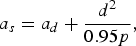 $${a_s} = {a_d} + \displaystyle{{{d^2}} \over {0.95p}},$$
Where, d is the diameter of metallic via holes connecting the upper and lower metallic layers of the bottom pyralux substrate. The via diameter (d) is taken by d = λ g/5 and pitch, i.e. center to center distance between the via holes is taken by p < 2d [Reference Wu, Deslandes and Cassivi15].
In Fig. 2 the top view of proposed membrane antenna along with longitudinal slot placed on the top ground plane of SIW structure is shown. Usually the distance from the short circuited end of SIW to the center of slot, i.e. d off2 is a quarter or multiple of quarter of the guided wavelength. Initially, this distance is chosen to be three quarter of the guided. Furthermore, the slot offset i.e. d off1 is optimized for proper excitation of longitudinal slot as well as the metallic patch antenna on the top layer. The initial dimension for longitudinal slot length is taken by [Reference Sourav, Asish and Anup13],
 $${L_s} = \displaystyle{{{\lambda _o}} \over {\sqrt {2\left( {{\varepsilon _r} + 1} \right)}}},$$
Fig. 2. Top view of SIW antenna along with rectangular slot.
The pyralux substrate with patch on top layer is supported by a layer of FR4 substrate having an optimized air gap of 1.8 × 1.8 mm under the MPA. The optimized dimensions for MPA are found to be 1.12 × 0.99 mm. The total size of antenna is found to be 10 × 10 mm. A conventional 50 Ω microstrip line is utilized as a feed element in the proposed antenna. The microstrip to SIW transition consisting of a tapered microstrip is also optimized for proper impedance matching. The detailed view of proposed single membrane antenna along with various important design parameters for MPA and air gap in FR-4 substrate are well explained in [Reference Vettikalladi, Saleem and Alkanhal16] and in Fig. 3.
Fig. 3. Top view of proposed membrane antenna geometry.
The optimum dimension for the proposed membrane antenna structure are W o = 0.145 mm, W t = 1.34 mm, L o = 1 mm, L t = 0.9 mm, d = 0.5 mm, p = 0.7 mm, a s = 1.5 mm, W s = 0.2 mm, L s = 1.225 mm, L = 3.5 mm, d off1 = 0.55 mm, d off2 = 1.4125 mm, L a = 1.85 mm, W a = 1.85 mm, L p = 1.15 mm, W p = 1.05 mm, L = 10 mm, and W = 10 mm.
III. RESULTS AND DISCUSSION
The proposed antenna structure is simulated and optimized using Ansys HFSS©. The results are further verified by simulating the proposed antenna structure in CST Microwave Studio.
A comparison between the simulation results of S 11 and gain obtained from HFSS and CST are given in Fig. 4. The two resonances at 92.4 and 95.5 GHz are due to presence of slot and patch in antenna geometry respectively, which are kept in close proximity to achieve wide impedance bandwidth. The FR-4 support with air gap plays an important role in merging the two resonances to achieve a wide impedance bandwidth. The antenna impedance bandwidth is found to be 5.4 GHz (91.5–96.9 GHz) from HFSS while from CST the impedance bandwidth is found to be approximately 4.9 GHz (91.5–96.4 GHz). The gain is found to be 7 dBi at the center frequency of 94 GHz. The peak gain of 7.5 dB is found at 95.5 GHz. Furthermore, the antenna gain remains above 6.7 dB in whole frequency band of operation.
Fig. 4. Simulated return loss S 11 and realized gain.
The antenna radiation pattern in both E-plane (horizontal plane) and H-plane (vertical plane) remains similar throughout the whole frequency band of operation. The comparison of two-dimensional (2D) radiation patterns obtained from HFSS and CST at 92, 94, and 96 GHz in both vertical plane (ϕ = 90°) and horizontal plane (ϕ = 0°) plane are shown in Figs 5 and 6 respectively. By increasing the ground plane size the small ripples in E-plane radiation pattern can be reduced, which are mainly due to diffraction of the limited ground plane. The cross-polarization ratio of less than −20 dB is achieved in E- and H-plane radiation patterns, respectively. The antenna 3 dB beam width is found to be 50° and 45° in E-and H-planes, respectively. For a better understanding the 3D radiation pattern for single element membrane antenna is shown in Fig. 7, whereas the wave propagating inside the SIW structure is illustrated by the electric field distribution plot as shown in Fig. 8.
Fig. 5. 2D radiation pattern in H-plane with co- and cross-polarization. (a) 92 GHz. (b) 94 GHz. (c) 96 GHz.
Fig. 6. 2D radiation pattern in E-plane with co- and cross-polarization. (a) 92 GHz. (b) 94 GHz. (c) 96 GHz.
Fig. 7. 3D radiation pattern of the proposed single antenna.
Fig. 8. Electric field distribution of the proposed single antenna.
IV. 1×4 ANTENNA ARRAY DESIGN
Figure 9 shows the top view of the proposed SIW-fed slot coupled 1 × 4 membrane antenna array. The four antennas are placed in horizontal plane (E-plane) improve the gain. The distance between the longitudinal slot is kept at d ar = 2.03 mm, i.e. 0.64λ0 where λ0 is the free space wavelength at 94 GHz. The array parameters such as slot length, slot width, patch length, patch width etc. are same as given in single element design in the previous section. The array is uniformly excited by a feed network to achieve maximum gain. The feed network consists of three identical 3 dB power splitters, each having a 50 Ω microstrip line connecting to two identical 70.7 Ω line for equal power transmission. The dimensions of microstrip lines for feed network are L 1 = L 3 = 2 mm, L 2 = 1.345 mm, L 4 = L1/2. The total array size is 16 × 11 mm. The top view of array along with some important parameter values is shown in Fig. 9.
Fig. 9. Top view of proposed 1 × 4 element array with, d ar = 2.03 mm, L a = 1.85 mm, W a = 8.14 mm, L 1 = 2 mm, L 2 = 1.345 mm, L 3 = 2 mm, and L 4 = 1 mm.
The return loss obtained from both HFSS and CST along with the gain is shown in Fig. 10. The array impedance bandwidth is found to be 5.2 GHz (91.3–96.5 GHz) from HFSS while from CST the impedance bandwidth is found to be approximately 4.2 GHz (92.5–96.7 GHz). The maximum gain is found to be 12.7 dB at 95.5 GHz whereas the overall gain of array is above 10.5 dB for the whole frequency band of operation. The estimated efficiency of the array is 76%.
Fig. 10. Simulated return loss S 11 and realized gain for 1 × 4 array.
The simulated E-plane radiation patterns from HFSS and CST at 92, 94 and 96 GHz are compared in Fig. 11. The array beam width in E-plane is found to be 20°. The cross-polar level is lower than −16 dB. The radiation pattern in H–Plane remains similar to as shown for the single element case. The 3D polar radiation pattern is shown in Fig. 12 for a better visualization of antenna array radiation pattern. Finally, the electric field distribution in antenna array is shown in Fig. 13.
Fig. 11. 2D radiation pattern in E-plane with co- and cross-polarization. (a) 92 GHz. (b) 94 GHz. (c) 96 GHz.
Fig. 12. 3D radiation pattern of proposed 1 × 4 array.
Fig. 13. The electric field distribution of the proposed 1 × 4 array.
V. CONCLUSION
The design and the results of a six layer membrane antenna/array based on SIW technology are presented. A MPA/array along with a longitudinal slot is utilized to achieve a wide impedance bandwidth of 5 GHz at center frequency of 94 GHz. The gain of the antenna for the single element is found to be above 6.5 dB in whole frequency band of operation and for the 1 × 4 array, it is found to be above 10.5 dB for whole frequency band of operation. Furthermore, similar antenna radiation patterns are achieved in whole frequency band of operation for single element, whereas for the 1 × 4 array the antenna beam width is reduced to 20° in E-plane while H-plane radiation patterns remains similar to that of a single element case. The proposed antenna finds applications in 94 GHz communication systems.
ACKNOWLEDGEMENT
The authors would like to thank King Abdulaziz City for Science and Technology (KACST) for providing fund through the Project no. ARP 34–137.
Hamsakutty Vettikalladi is an Assistant Professor in the Department of Electrical Engineering, King Saud University Since November 2012. He started his carrier as a Postdoctoral researcher at the Bell Engineering Department, University of Arkansas, USA in January 2008, just after finishing his Ph.D. from Cochin University of Science and Technology. Later, he moved to Institute of Electronics and Telecommunication of Rennes, University of Rennes1, France. His main research focus includes microwave and millimeter wave antenna design for various applications including high-speed WIFI, automotive radar, imaging, point to point communication for 4G/5G. He worked with many projects from various companies such as CANON-France, Bouygues Telecom-France, VALEO Germany, and Thales aerospace in France. He has served as visiting faculty, editor, and referee in several institutes and scientific journals and conferences. He is the author of more than 58 research publications in well-reputed international journals and conferences and one book chapter.
Muhammad Kamran Saleem received his B.Sc. degree in Electrical Engineering from the Mirpur University of Science and Technology (MUST), Pakistan in 2005 and M.Sc. degree in Telecommunications Engineering from Blekinge Institute of Technology (BTH), Sweden, in 2007. Currently, he is working toward the Ph.D. degree in King Saud University (KSU), Saudi Arabia. From 2007 to 2011 he worked in Pakistan space agency, where focus of his research was on microwave waveguide components for satellite payloads, during his stay there he was awarded the annual research excellence award twice in 2009 and 2010, respectively. In 2014, he was awarded the best Ph.D. student award. His research interests include waveguide filters, microwave and millimeter wave antennas, reconfigurable antennas, and dielectric resonator antennas.
Majeed A. S. Alkanhal is a full professor in The Department of Electrical Engineering at King Saud University, Riyadh, Saudi Arabia. He received his Ph.D. in Electrical Engineering from Syracuse University, Syracuse, New York in 1994. His research interests include wireless communications, radar systems, electromagnetic propagation and scattering in complex materials, microwave/millimeter-wave antenna design and optimization, modern optimization techniques, and computational electromagnetics. Professor Alkanhal has served as consultant, visiting scholar, editor, and referee in several institutes and scientific journals. He has published books, book chapters, research papers, technical reports, and patents in his fields of research interests.

