Introduction
The Vivaldi antenna, introduced by Gibson [Reference Pozar1, Reference Gibson2], is an aperiodic continuously scaled traveling wave antenna. It is a planar antenna which can be designed for high directivity, narrow beam-width and high-power density radiation in the X-band frequency range. Due to its planar profile, it is very useful in a complex integrated microwave circuit, which is used in satellite communications, earth-detection radar, EM measuring instruments, and biomedical equipment. It can be designed for three different tapered profiles, linearly tapered slot antenna (LTSA), constant width slot antenna (CWSA), and exponentially tapered slot antenna (ETSA), where each profile has a different radiation characteristic. The beam-width of these three profiles (ETSA, LTSA, and CWSA) is decreasing whereas the side lobe level is found increasing in order from left to right [Reference Lewis, Fassett and Hunt3, Reference Schaubert, Kollberg, Korzeniowski, Thungren, Johansson and Yngvesson.4]. In further investigation, an antipodal slot line transition is incorporated in the exponential slot of the Vivaldi antenna. The resulting structure of the antipodal Vivaldi antenna provides a broad bandwidth which is very useful in many microwave imaging applications [Reference Gazit5–Reference Kim and Chang8]. Due to its wide-range of applications, the Vivaldi antenna has always been a research interest and studied for the improvement of output parameters like bandwidth, voltage standing wave ratio (VSWR), directionality, beam-width, cross polarization etc. Various studies in this reference have been presented in the earlier literature [Reference Shuppert9–Reference Wan Ahmad Khairuddin, Othman, Misran, Abd. Aziz, Sulaiman and Kamarudin15].
This paper presents the design and fabrication of a novel patch compensated wideband Vivaldi antenna in the frequency range of 6.0–8.0 GHz. Initially, an optimized computer-aided design of the Vivaldi antenna has been developed, optimized, and simulated where the obtained results are analyzed for the desired radiation parameters in terms of the VSWR, bandwidth, directionality, and beam-width. This optimized design has been fabricated and tested; wherever results are not found as desired. The finding reveals that the problem is possibly associated with a discontinuity at the feed line, fabrication tolerance constraints and parasitic capacitance at the edges or the bent of the microstrip feedline which introduce the parasitic reactance. Due to the parasitic reactance, the results of the fabricated antenna deteriorates. Therefore, the study presented in this paper is based on the investigation of compensation theory for associated discontinuity. This explores a generalized theoretical procedure for the compensation of an associated problem. The developed theory has been applied in fabrication and tested for the desired results. The applied technique involves an incorporation of a small patch into the feed line for the compensation of the associated problem which has no effect on other design parameters of the antenna. This is the main advantage of the theory. The earlier works [Reference Gazit5–Reference Kim and Chang8] applied for compensation in antenna design itself which leads to various problems like cross polarization, impedance mismatching, shifting of antenna band at any side of the center frequency. The devised procedure can be applied in the fabrication of the Vivaldi antenna for different specifications. This paper is structured as follows.
In section ‘Design and simulation of Vivaldi antenna’, design and simulation of the Vivaldi antenna are described whereas fabrication and testing of results are explained in section ‘Fabrication & testing’. Section ‘Compensation of Vivaldi antenna using the patch on feeding line’ explores a novel compensation technique that is applied in the fabrication of the Vivaldi antenna to achieve the desired results. The detailed result and discussion are explained in section ‘Results and discussion’. The conclusion of the work is given in section ‘Conclusion’.
Design and simulation of the Vivaldi antenna
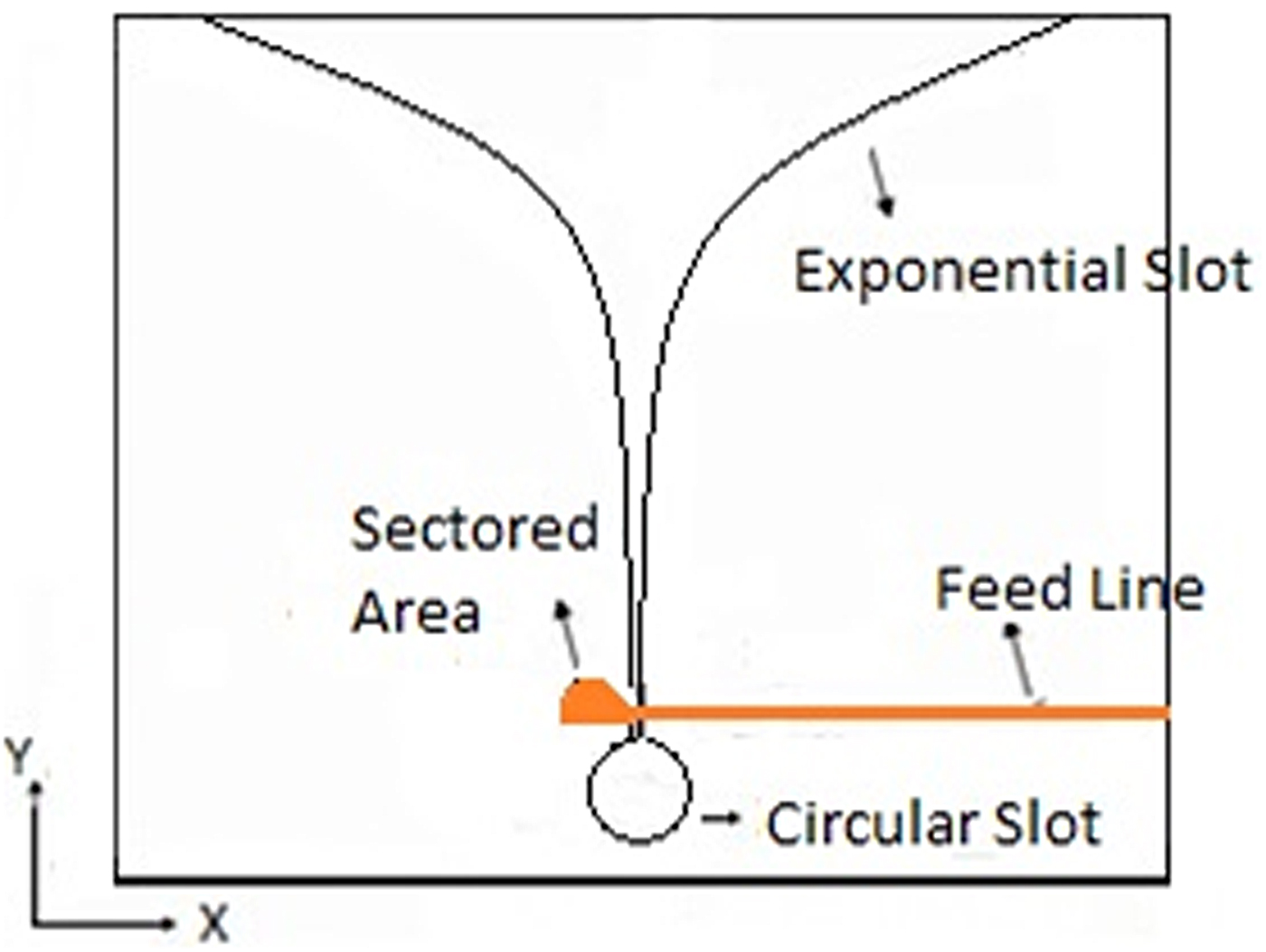
The Vivaldi antenna is a planar antenna that is fabricated on a microstrip feedline with an exponentially tapered slot profile. Fig. 1 shows a comprehensive design of the Vivaldi antenna where the dimension of the antenna slot profile is given on the printed circuit board (PCB) base. A microstrip feeding line with a terminated sector-shaped area is used to excite the circular space. The signal from the circular resonant slot reaches the antenna aperture through an exponential slot followed by a symmetrical slot line. The antenna is designed with three types of slots, circular, rectangular, and exponential with their own functionalities. The circular slot used to tune the antenna for different resonant frequencies, which can be achieved by changing the dimension of the slot. The rectangular slot works as a slotted waveguide which is used to transmit an electromagnetic wave from the circular slot to antenna aperture while the exponential slot provides a transition between the antenna aperture and rectangular slot. As per theoretical study, the length of the antenna must be greater than the average wavelength in the operating frequency band. Also, the antenna width must be greater than half of the lowest working frequency [Reference Gibson2, Reference Shin and Schaubert11]. The brief description of the theoretical study used in the design calculations is discussed as follows [Reference Collin16].

Fig. 1. Design of Vivaldi antenna.
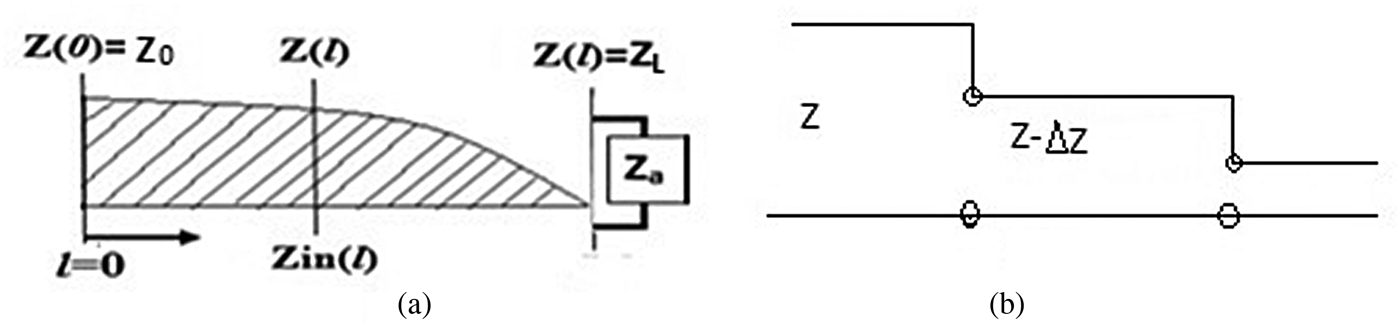
A schematic of the one side of the tapered assembly is shown in Fig. 2(a), where Z a is the antenna load impedance, Z 0 is the characteristic impedance of a uniform slotted waveguide, l is the total length of the exponential profile, β is the propagation constant of the slot line and Γ represents the equivalent reflection coefficient of load impedance at distance l.

Fig. 2. (a) Block diagram depicts the impedance variation for exponential slot w.r.t. length. (b) Diagram depicts the tapered line composed of decremented sections.
The equivalent of a continuously tapered line, as shown in Fig. 2(b), is made up of several decremented sections of length ΔZ. The change of the reflection coefficient from the step z is given by
 $${\rm \Delta \Gamma} = \displaystyle{{\left( {Z - {\rm \Delta Z}} \right) - z} \over {\left( {Z - {\rm \Delta} Z} \right) + z}} \cong \displaystyle{{{\rm \Delta} Z} \over {2Z}}\;.$$
Substituting ΔZ → 0 for a small element, the above equation can be written as
 $$d{\rm \Gamma} = \displaystyle{{dZ} \over {2Z}} = \displaystyle{1 \over 2}\displaystyle{{d({\rm ln}Z/Z_0)} \over {dZ}}\;.$$
Since
 $$\displaystyle{{d({\rm ln}f\,(z))} \over {dZ}} = \displaystyle{1 \over f}\displaystyle{{df\,(z)} \over {dz}}\;.$$
Using the theory of small reflections, the total reflection coefficient at z = l can be calculated by integrating the partial reflection coefficients with their appropriate phase shifts given by
 $${\rm \Gamma} \left( \theta \right) = \displaystyle{1 \over 2}\mathop \int \limits_{Z = 0}^L e^{ - 2j\beta z}\displaystyle{d \over {dZ}}{\rm ln}\left( {\displaystyle{Z \over {Z_0}}} \right)dz.$$
The impedance of the exponentially tapered section is expressed as
 $$\; Z\left( z \right) = Z_0e^{az},\; \; \quad {\rm \; for}\; 0 < Z < L.$$
Constant a can be determined by applying the boundary condition at l = 0, Z(0) = Z 0 ; and L = l, Z(L) = Z L = Z 0e aL, as shown in Fig. 2(a)
 $$a = \displaystyle{1 \over L}ln\left( {\displaystyle{{Z_L} \over {Z_0}}} \right)\;. $$
By substituting the value of Z/Z 0 in equation (6)
 $${\rm \Gamma} = \displaystyle{1 \over 2}\mathop \int \limits_{Z = 0}^L e^{ - 2j\beta z}\displaystyle{d \over {dZ}}{\rm ln}(e^{az})dz.$$
This gives
 $${\rm \Gamma} = \displaystyle{{{\rm ln}Z_L/Z_0} \over 2}e^{ - j\beta L}\displaystyle{{\sin \beta L} \over {\beta L}}\;. $$
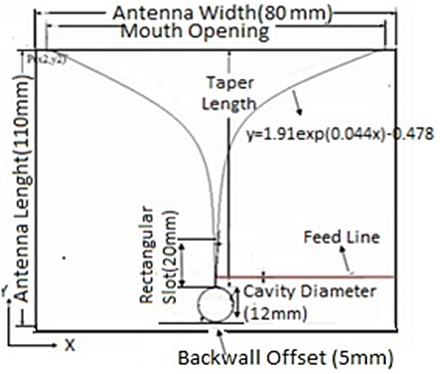
Equation (8) derives the relation between the reflection coefficients, Γ, at any arbitrary location l on the tapered profile. Based on this relation, the length and exponent of the slot profile can be calculated for the defined values of Γ and load impedance Z L. The dimensions of the Vivaldi antenna has been calculated and optimized using COMSOL software for the desired radiation parameters, whereas the final drawing of the Vivaldi antenna is shown in Fig. 3.

Fig. 3. Detailed drawing of Vivaldi antenna.
Concept of microstrip-to-feedline transition
In the Vivaldi antenna, the excitation to the rectangular slot is given through a microstrip feed line. A microstrip-feed transition is shown in Fig. 4. The slot and microstrip feed line are etched on different sides of the substrate. The rectangular slot is excited by the coupling effect from the feedline. Circular stubs are used for the proper coupling of feed from the feedline to the slot [Reference Shuppert9]. Their geometry makes a right angle. Both the microstrip feedline and slot extend a quarter of the wavelength which can be clearly seen in Fig. 4.
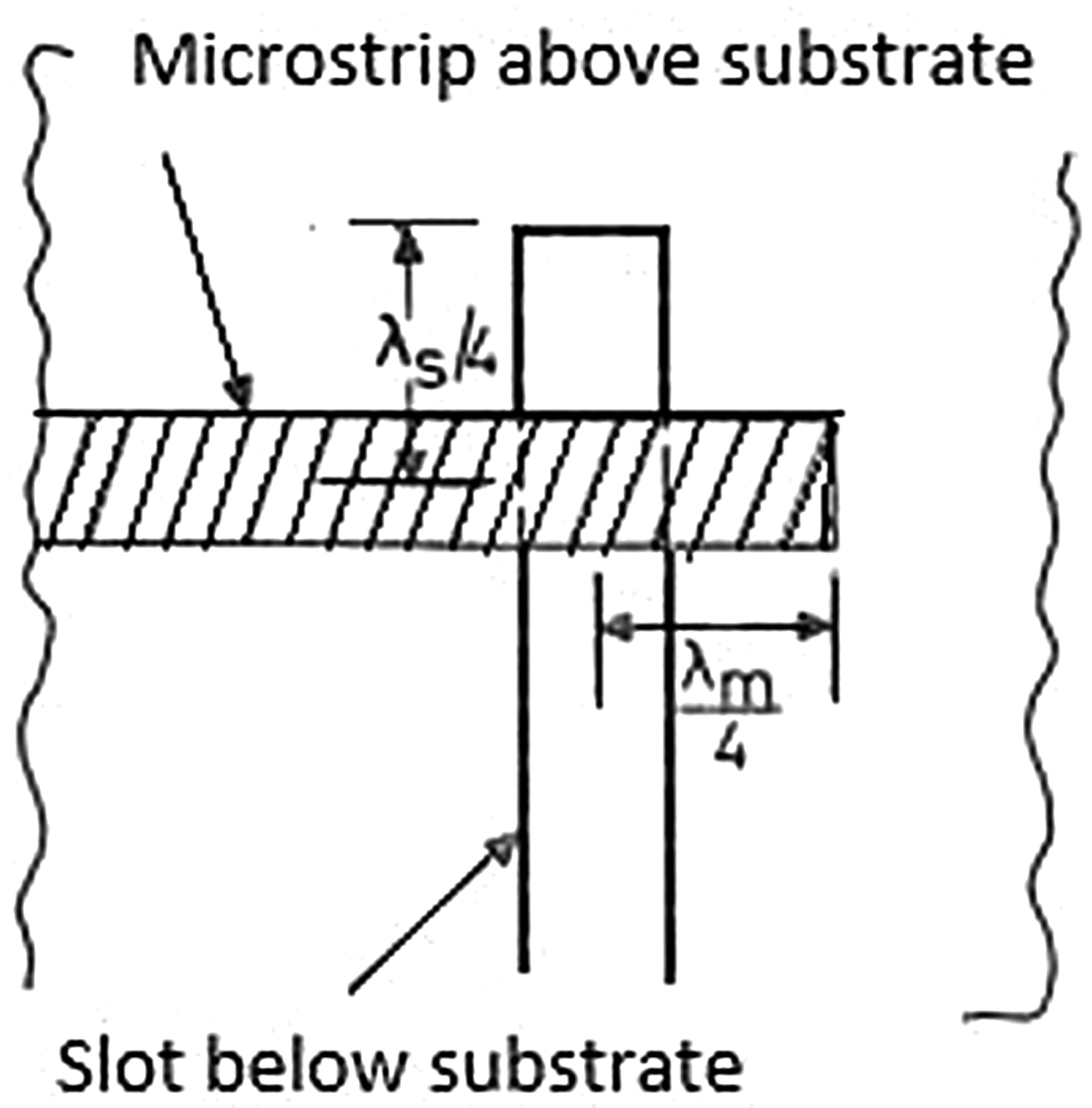
Fig. 4. Schematic of microstrip feedline to slot transition.
An equivalent circuit of the above stated transition is shown in Fig. 5. X OS represents the inductance of the slot, whereas C oc is the capacitance of an open microstrip feedline. Z OS and Z OM are slot and microstrip feedline impedances, respectively. θ s and θ m represent the electrical lengths of the extended portions of the slot line and the microstrip feedline, respectively.
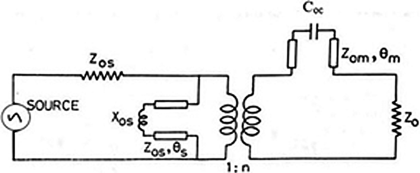
Fig. 5. Equivalent circuit diagram of the microstrip feedline to slot transition.
The design of the Vivaldi antenna shown in Fig. 3 has been simulated and analyzed using COMSOL Multiphysics which is presented in Figs 6 and 7. The Vivaldi antenna is designed for the operating frequency of 7.5 GHz and providing a bandwidth in the frequency range of 6.0–8.0 GHz.

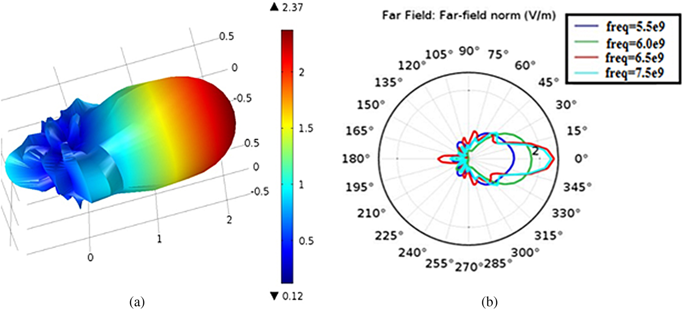
Fig. 6. (a) 3D view of the far-field radiation pattern of Vivaldi antenna. (b) The 2D polar plot of the radiation pattern of Vivaldi antenna.

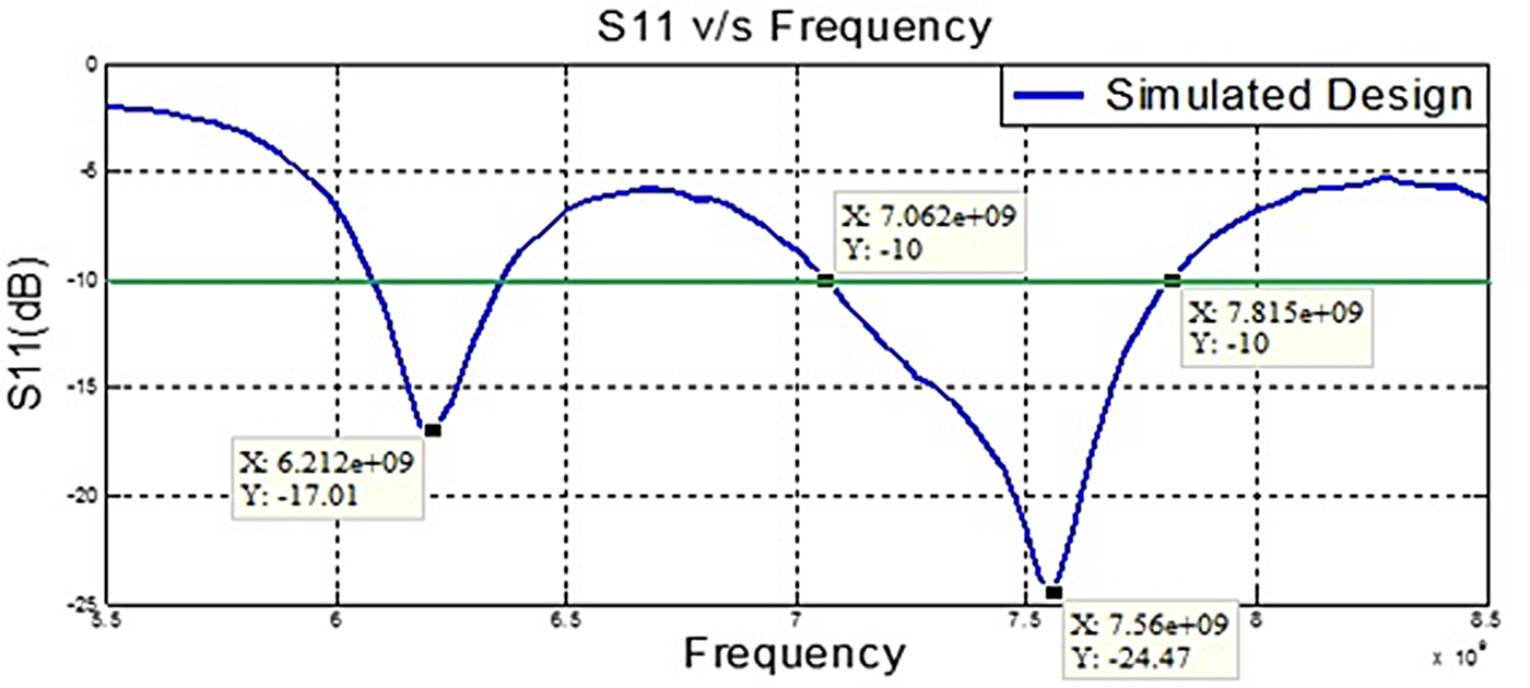
Fig. 7. Plot representing S 11 of Vivaldi antenna design simulated on COMSOL.
Simulation results in terms of the radiated electric field are shown in Fig. 6, where Figs 6(a) and 6(b) represent the 3D and 2D plot of the radiated field, respectively. In Fig. 6(b), the radiation characteristics are given for variable operating frequency and presented in a comparative manner. The result shows as frequency increases the beam-width of the radiated electric field becomes narrower and more directional. The return loss characteristic of the antenna is shown in Fig. 7, which provides a return loss better than 15 dB in the given bandwidth of 7.06–7.81 GHz. These values are desirable in the fabricated antenna.
Fabrication & testing
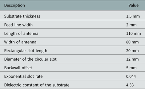
The designed model has been fabricated on a PCB alumina substrate with a dielectric constant of 4.33 and a substrate thickness of 1.5 mm. A very thin layer of alumina (~1.5 µm) is coated on a substrate which has been itched as per dimension is given in Table 1 for the final fabrication of the Vivaldi antenna.
Table 1. List all the important parameters taken into consideration while designing of Vivaldi Antenna
The photograph of the front and back view of the fabricated Vivaldi antenna is shown in Fig. 8. The front view expresses the main design of the antenna on the metallic side of the PCB whereas, in the back side of the PCB, the feed line is shown. At the end of the fed line, the sector-shaped area is fabricated to provide the capacitive coupling of an electromagnetic wave with the circular slot.
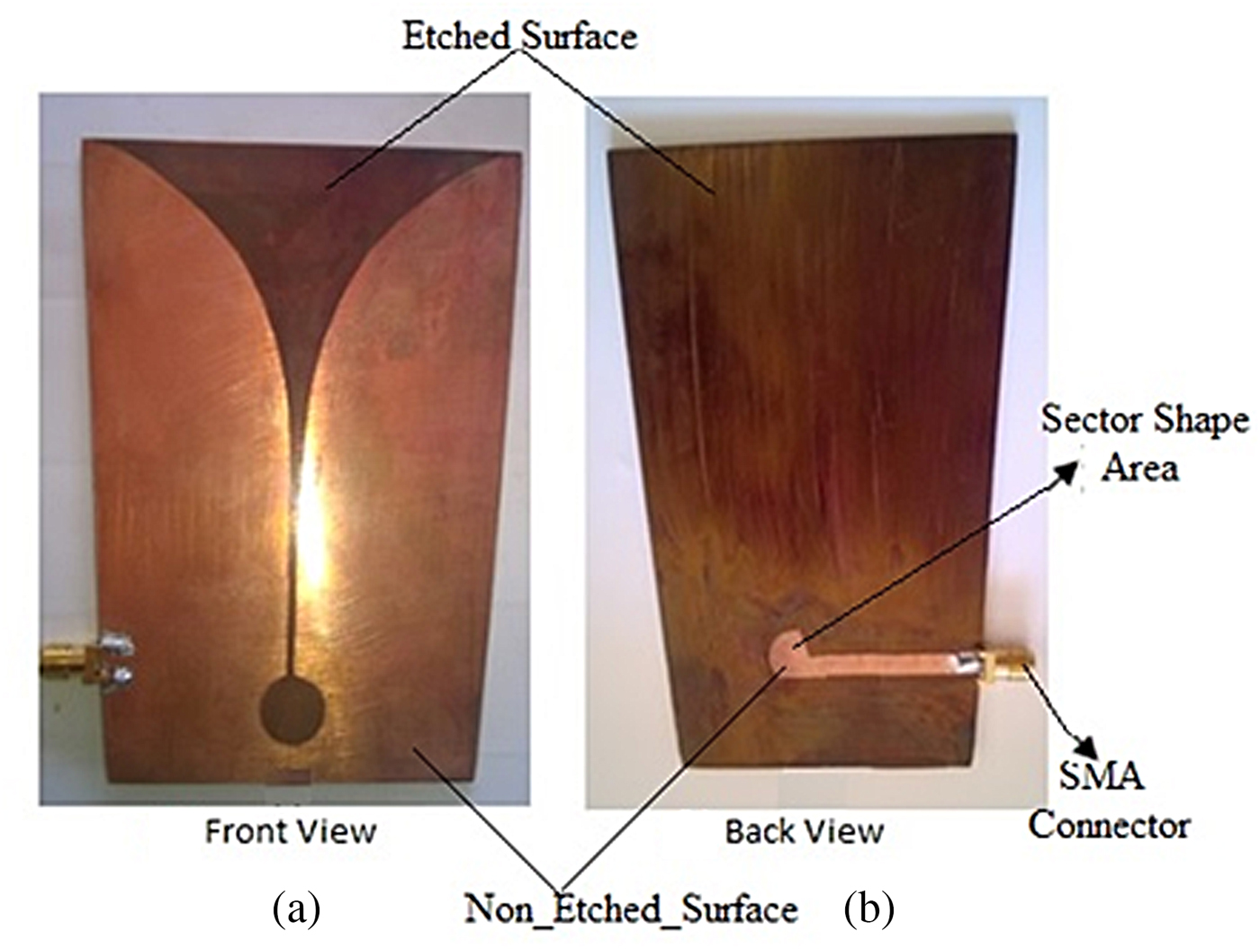
Fig. 8. Front and back view of Vivaldi antenna fabricated on PCB.
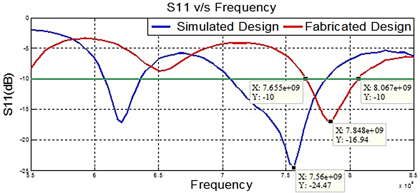
The fabricated design is tested with a vector network analyser (VNA) where a perspective comparison of the test and simulation result is shown in Fig. 9. This shows that the return loss of the fabricated antenna in the prescribed band is found to be inferior to the simulation results. The above ambiguity has been analyzed and found associated with the fabrication constraint and discontinuity present at feeding lines. The compensation of the associated discontinuity is inevitable for having the desired result in the prescribed band. Therefore, a theoretical procedure has been developed to compensate and improve the performance and explained in next section.

Fig. 9. S 11 comparison plot for the fabricated design with simulation design.
Compensation of the Vivaldi antenna using the patch on feeding line
Further investigation considers that the mismatching of the Vivaldi antenna is associated with the cause of discontinuity at the feeding point, fabrication tolerance and associated parasitic capacitance at edges or bent of the microstrip feedline which introduces the parasitic reactance in antenna design [Reference Yadav, Kumar and Kulkarni17, Reference Yadav, Kumar and Kulkarni18]. Thus, the antenna impedance is mismatched from the radiofrequency source which should be essentially matched for better radiation. For this reason, test results are found deteriorated from the simulation results. A theoretical procedure has been developed for the compensation of these associated problems.
The theory explores that the mismatching of the antenna can be compensated by using a reactive patch on feed lines. The patch is a small segment of the strip line, which introduces a reactive equivalence in the feed line. The equivalent circuit of the antenna including source, feed line, and the inductive section is shown in Fig. 10. Antenna impedance is Z A which is different from the impedance of the feed line Z 0 = 50 Ω. Z B and Z C have transferred impedances of the antenna at points B and C on the feed line, respectively. A strip line patch of length l = λ/12 and impedance Z P is introduced in the feed line for compensation of antenna impedance where the impedance, Z P , is taken as ≫ Z B.
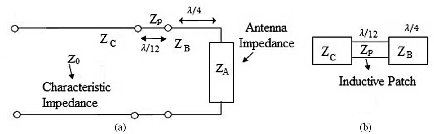
Fig. 10. (a) Equivalent circuit diagram for the impedance offered by the reactive path of feedline. (b) Block diagram depicts the impedance offered by the reactive path of antenna feedline.
From Fig. 10(a) Z B and Z C can be expressed as
 $$Z_B = \sqrt {Z_A}, $$
 $$Z_C = Z_p\left( {\displaystyle{{Z_B + jZ_p{\rm tan}\left( {\beta l} \right)} \over {Z_p + jZ_B{\rm tan}\left( {\beta l} \right)}}} \right),$$
Here impedances Z A and Z B are normalized at the characteristic impedance Z 0.
For l < λ/10, Z B ≪ Z p, term tan βl ≈ βl, is incorporated into equation (10)
 $$Z_C = Z_p\left( {\displaystyle{{Z_B + jZ_p\left( {\beta l} \right)} \over {Z_p + jZ_B\left( {\beta l} \right)}}} \right).$$
The above can be approximated for Z p ≫ Z Btan(βl), now
 $$Z_C = Z_p\left( {\displaystyle{{Z_B + jZ_p\left( {\beta l} \right)} \over {Z_p}}} \right),$$
 $$Z_C = Z_B + jZ_p\left( {\beta l} \right).$$
 $$Z_C = \sqrt {Z_A} + jZ_p\left( {\beta l} \right).$$
From equation (14), it can be observed that the patch behaves as inductive and introduces reactance of Z p(βl) that is added to the antenna impedance which can be changed by changing any one of parameters, Z P or l. Thus, the antenna can be matched by compensating the reactive patch. This procedure provides a method by which the compensation of the antenna can be made without affecting the original design of the antenna.
As we know, a slot antenna is equivalent to the magnetic dipole at its first resonant frequency at the guided wavelength. This resonance becomes broader by incorporating exponential tapering in the slot which we are using in the Vivaldi antenna. Here, the incorporated reactive patch introduces a fictitious secondary resonance which can be planted in the desired band in support of the primary resonance by having a proper choice of dimension and location. The combine effect of these two resonances improves the bandwidth and return loss parameter of the antenna. This fact can be described with the help of the following analysis. From equation (8), reflection coefficient Γ at point A is taken as
 $${\rm \Gamma} = \displaystyle{{Z_A - 1} \over {Z_A + 1}} = \displaystyle{{{\rm ln}Z_L/Z_0} \over 2}e^{ - j\beta L}\displaystyle{{\sin \beta L} \over {\beta L}}\;. $$
This gives
 $$Z_A = \displaystyle{{1 + {\rm \Gamma}} \over {1 - {\rm \Gamma}}}. $$
By using equations (14) and (16) impedance at point-P, Z P can be derived as
 $$Z_p = \sqrt {\displaystyle{{1 + {\rm \Gamma}} \over {1 - {\rm \Gamma}}}} + jZ_p\left( {\beta l} \right).$$
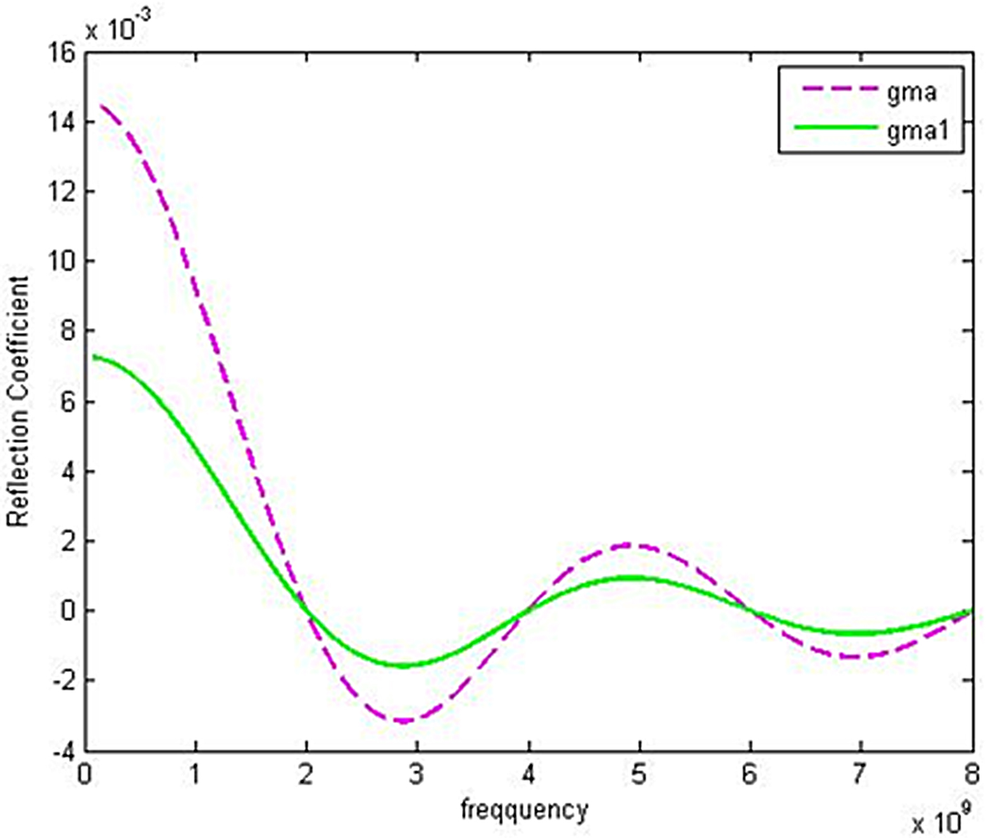
Here Z P represents the impedance of the antenna appearing at point P, by using this equation, the reflection coefficient at point P, Γ1 can be derived. The reflection coefficients Γ1and Γ have been plotted in the range of 0.1–10.0 GHz shown in Fig. 11, where parameters, β = 2π/λ 0, normalized patch and load impedance Z p,and Z L are 2.0 and 7.5, respectively, are taken.

Fig. 11. Perspective comparison of reflection coefficients before and after compensation.
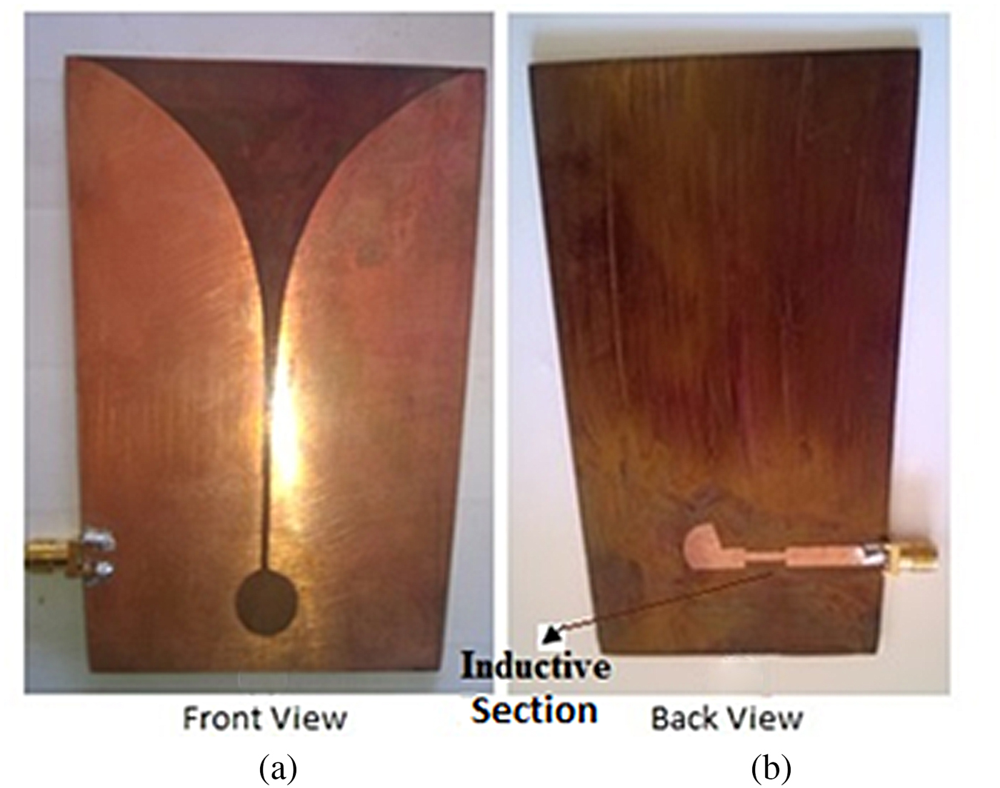
Here λ 0 is the wavelength at the center frequency f 0. From Fig. 11, it can be observed that the reflection coefficient is reduced overall. Therefore, the theory has been applied in the fabrication and photograph of the compensated antenna shown in Fig. 12, where a small inductive section is fabricated on the feedline. The test results compensated antenna is explained in the next section in comparison with earlier test and simulation results.

Fig. 12. Fabricated design of Vivaldi antenna (a) front view. (b) Back view showing feeder compensation (inductive section on feedline).
In uncompensated design, the impedance offered by the SMA Cable is 50 Ω, which is transferred through the SMA connector to the feedline. In design, the impedance of the feedline is 50 Ω whereas the antenna impedance is >50 Ω. To match the impedance factor, a reactive section is incorporated in the design part where the antenna is fed by the backward microstrip feedline technique. Hence, by this technique there should be proper matching of impedance, to couple the feed to the circular slot of the antenna.
Results and discussion
The proposed compensation has been incorporated in the fabrication of the antenna and tested with the VNA.
The comparison of the S 11 plot of the simulated design of the inductive section feedline on COMSOL with the fabricated inductive section feedline antenna design is presented in Fig. 13. The result clearly justifies that the reason behind the non-ideal performance of the fabricated antenna against simulation is due to the feedline. Therefore, the proposed compensation is within the appropriation of the above said theory.
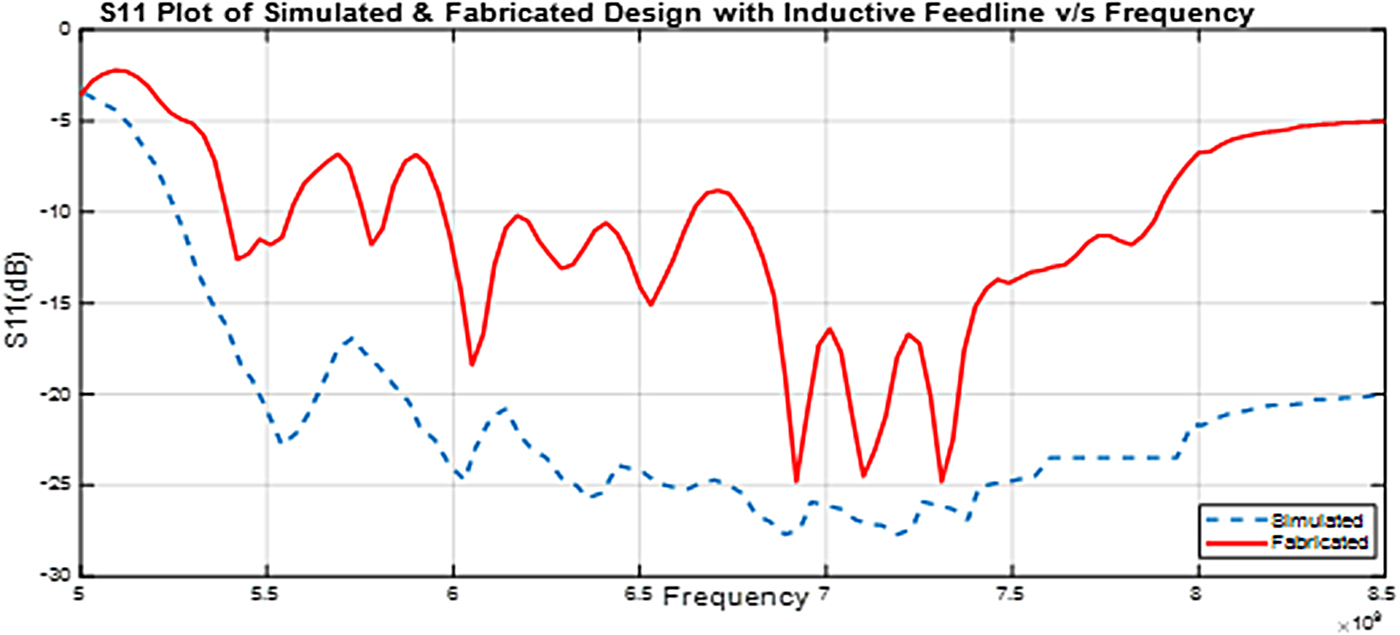
Fig. 13. Depicts the S 11 plot for the simulated design of inductive feedline compared with the S 11 plot for the fabricated inductive feedline antenna design.
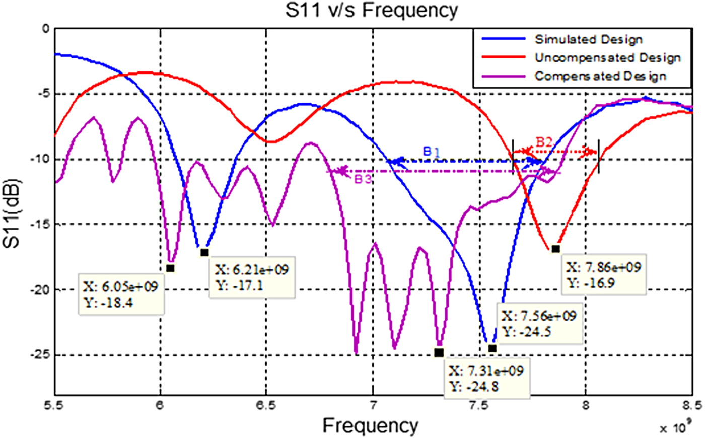
A comparative study of test and simulation results is shown in Fig. 14. From the results, it can be observed that in the given frequency band, the center frequency of the uncompensated antenna is shifted right side and overall return loss parameter, S 11 is found inferior to the simulation result. The bandwidth of the uncompensated antenna, B 2 (7.65–8.06 GHz), was also found narrower to the simulation result B 1 (7.06–7.81 GHz).

Fig. 14. The S 11 plot for the compensated designs plotted against conventional design.
As the compensation in the feed line is incorporated, the test result is found providing better return loss parameter in the entire frequency band as compared to the simulation and test results of the uncompensated antenna. Here, the center frequency is also found shifted toward the left side and provide wider bandwidth B 3 (6.77–7.89 GHz) as compared to B 1 and B 2. This also covers the desired operating band B 1 along with a center frequency, i.e. 7.5 GHz, as we obtain in the simulation result. It can be observed that the applied compensation not only provides better return loss but also provides a better bandwidth in the desired range. The parameters obtained from the compensated antenna are compared with simulation and test results of the uncompensated antenna and shown in Table 2.
Table 2. Comparative observation deduced based on S 11 Plot
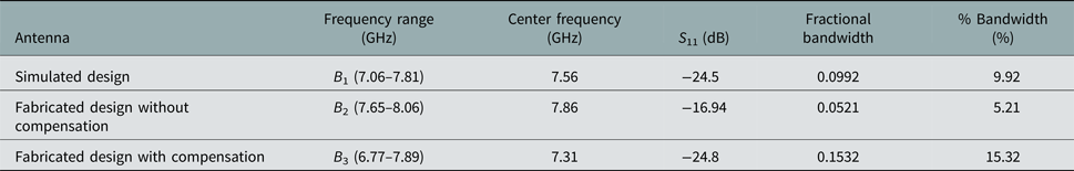
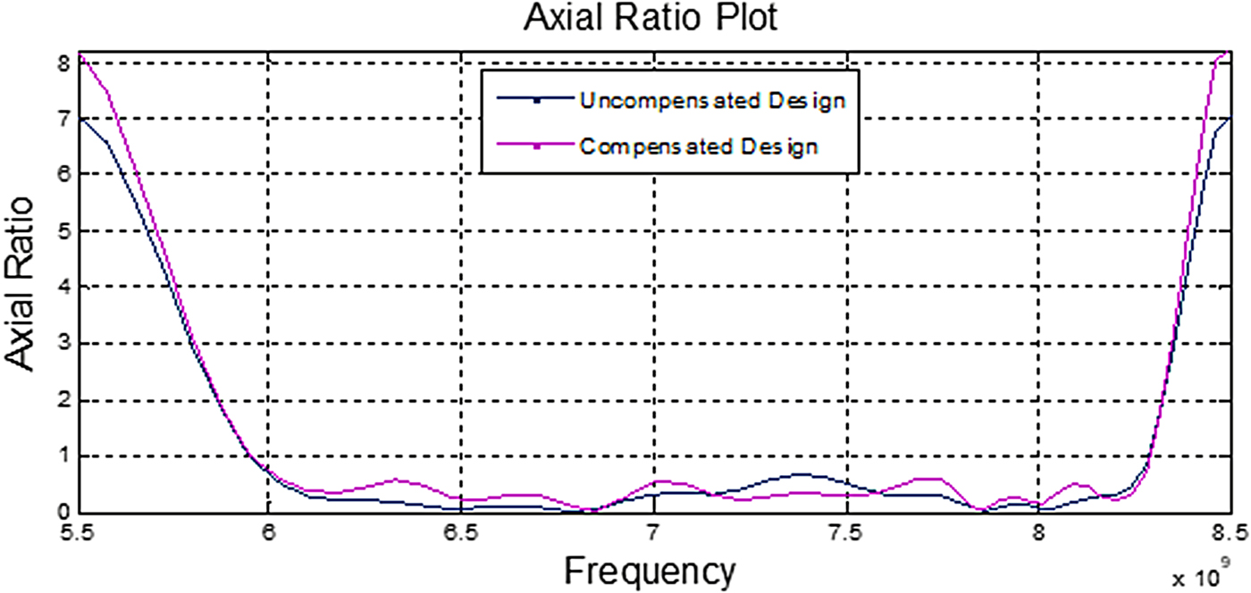
Figure 15 presents the axial ratio plot for the uncompensated and compensated antenna design. It can be observed that the axial ratio of both is found similar in the band. This means that the patch compensation design does not affect polarisation.

Fig. 15. Axial ratio plot for compensated design plotted against uncompensated design.
Conclusion
Design and development of the patch compensated wideband Vivaldi antenna is presented in the paper. The presented work mainly highlights the problem associated with the development of the Vivaldi antenna, due to the discontinuity at the feeding point, fabrication tolerance and parasitic capacitance at the edges or the bent of the microstrip feedline. A theoretical procedure has been developed for the compensation of these effects. The developed theory explores that the associated effects can be compensated by incorporating the inductive patch on the feed line. This theory has been applied in fabrication which effectively compensates the associated problems tested for the desired results. In the devised technique, compensation is incorporated in the feed line, whereas the other design parameters of the antenna are unaffected. This is the main advantage of the presented work.
Acknowledgements
The authors would like to thank Prof. Rajesh Khanna of Electronics and Communication Engineering Department for his kind support during the testing of the antenna with VNA.
 Dr. Rana Pratap Yadav received his M. Tech. degree in 2009 from the NIT Bhopal and received his Ph.D. from the Homi Bhabha National Institute (HBNI), Mumbai in 2014. He has joined the Thapar Institute of Technology, (TIET) as Assistant Professor in 2014. Currently, he is working at the University of Oxford as a Postdoctoral Researcher. His current research is focused on the development of an efficient harmonics radar system for tracking of small targets.
 Dr. Vinay Kumar received his Bachelor of Engineering in 2000 and received his Ph.D. at the Jaypee University of Information Technology in 2009. He is currently working in Electronics and Communication Engineering department at the Thapar Institute of Engineering and Technology.
 Rajveer Dhawan received his Bachelor of Engineering in 2014 and received his M.E. degree in Wireless Communication from the Thapar Institute of Engineering and Technology (TIET) in 2016. His research is based on the design, optimization and fabrication of patch compensated wideband Vivaldi antenna and its analysis in RADOME chamber.