I. INTRODUCTION
Power dividers (PDs) are key devices in communication systems for differential power amplification or antenna arrays feeding purposes. Wilkinson PDs constitute efficient components thanks to high isolation between the output ports, and easy design when dealing with planar structures [Reference Wilkinson1, Reference Pozar2].
However, they suffer from a lack of flexibility, (i) when connecting the resistance necessary for isolation between the output ports, and (ii) in the choice of the characteristic impedance of the quarter-wave length arms. They also suffer from a large surface area, with two quarter-wave length transmission lines (TLines). In [Reference Horst, Bairavasubramanian, Tentzeris and Papapolymerou3], the authors added extra TLines for connecting the isolation resistance. This avoids parasitic coupling between the two out ports, which constitutes a real drawback when dealing with millimeter-wave frequencies. More recently, a general model was developed to give design rules for the synthesis of these additional TLines [Reference Okamura, Wang, Takahashi, Tahara and Sakagami4]. A large variety of characteristic impedances can be chosen in such a way that various power ratios between the out ports can be reached. In [Reference Ahn5], the quarter-wave length arms of the conventional impedance transformer were miniaturized thanks to the use of open stubs and/or step impedances. This also enhanced flexibility in the choice of the TLines characteristic impedance. In counterpart, this topology leads to a complex impedance transformation instead of the classical real one. Hence, a capacitance must be added in series with the resistance of the isolation branch so as to compensate the imaginary part.
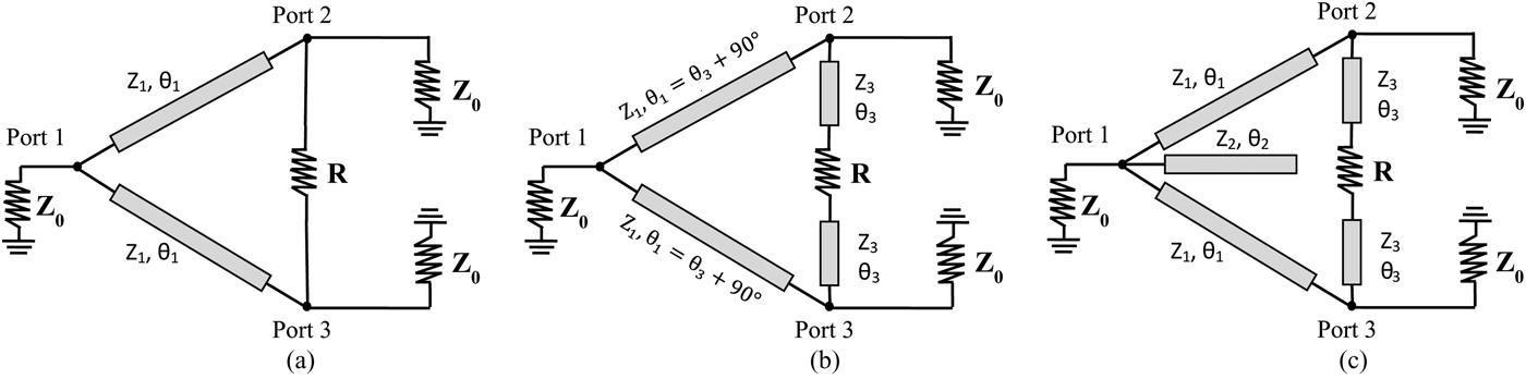
Miniaturization and flexibility in design are of higher interest. Size reduction is important, for cost reasons, at RF frequencies in PCB technologies, and, even more important, at millimeter-waves in CMOS technologies, where distributed circuits based on TLines are used, as explained in [Reference Horst, Bairavasubramanian, Tentzeris and Papapolymerou3]. In that case, the PDs must be both efficient and compact, and offer design flexibility. In particular, the choice of the characteristic impedance of the TLines is critical. As discussed in [Reference Franc, Pistono, Corrao, Gloria and Ferrari6], the quality factor of the TLines realized in the Back-End-Of-Line of a CMOS technology strongly depends on their characteristic impedance. It is thus mandatory to develop flexible topologies for which the optimal characteristic impedance can be chosen. In this context, PDs proposed in [Reference Horst, Bairavasubramanian, Tentzeris and Papapolymerou3] suffer from their bigger surface compared with the classical Wilkinson one (Fig. 1(a)). This is due to the extra length of TLines 1 since θ 1 = θ 3 + 90°, as shown in Fig. 1(b). Capacitive or stub loading at the three ports of Fig. 1(a) enables size reduction, 53 or 74%, respectively, as shown in [Reference Scardelletti, Ponchak and Weller7, Reference Wu, Li and Guo8]. A design procedure was proposed in [Reference Scardelletti, Ponchak and Weller7] but it did not consider the isolation resistance feeding TLines. Another solution based on a П-type stub in the parallel arms, instead of classical TLines, reduces the PD size as well [Reference Tseng and Wu9]. However, such PDs need TLines with high characteristic impedance, which constitutes a drawback with CMOS technologies. Besides, the design is complicated by a strong meandering to get high miniaturization. Hence, no solution includes at the same time flexibility, reduced-size, and high-performance.

Fig. 1. (a) Wilkinson PD. (b) Modified PD [3]. (c) Modified PD with open stub, the proposed solution.
In this paper, it is shown that flexibility and high-performance can be addressed simultaneously. The novel design method proposed by the authors consists in searching sets of solutions that enable to reach targeted high electrical performances. The authors developed simple design equations to extract three essential design parameters, which could potentially become solution sets. They also demonstrated that one criterion is enough to complete the search for solutions. Theory and design equations are addressed in Section II. Then a design procedure is described in Section III, and finally experimental results are given in Section IV, showing a very good agreement between measurement and simulation results. They are compared with others' work in Section V.
II. THEORY AND DESIGN EQUATIONS
Figure 1(c) gives the proposed PD topology. Compared with the one presented in [Reference Horst, Bairavasubramanian, Tentzeris and Papapolymerou3] (Fig. 1(b)), an open stub of characteristic impedance Z 2 and electrical length θ 2 was added at port 1. The characteristic impedance and electrical length of the arms between ports 1 and 2 (or ports 1 and 3) were named Z 1 and θ 1, while the ones connecting the output ports to the resistor were named Z 3 and θ 3. When both TLine (Z 3, θ 3) and open stub (Z 2, θ 2) are used, perfect matching at all ports and perfect isolation cannot be achieved. However, they can be brought close to zero by means of the design procedure explained in the next section. Matching and isolation will be slightly degraded compared with the classical Wilkinson topology, but the corollary will be an extended bandwidth as demonstrated by Fano, as a general rule and for any kind of circuit, in [Reference Fano10].
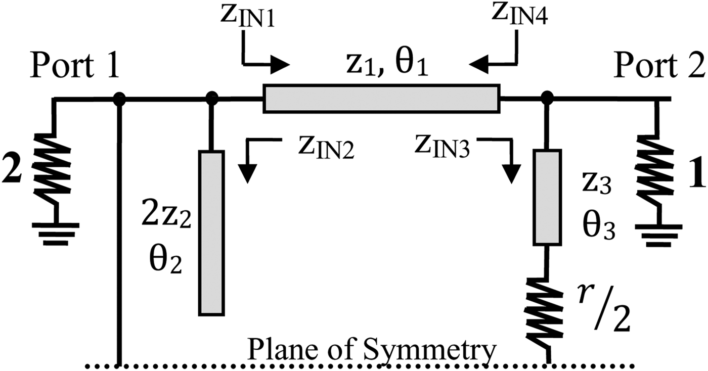
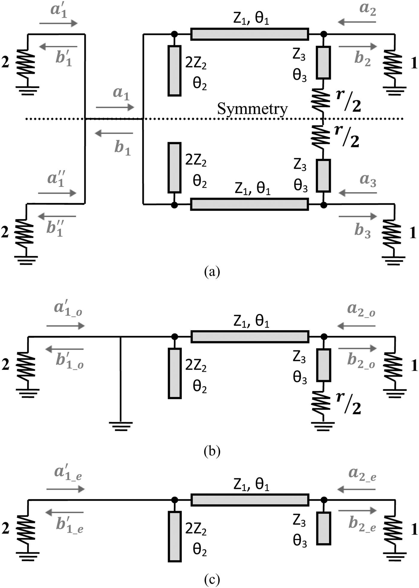
For simplicity, all the characteristic impedances were normalized to the system characteristic impedance Z 0, i.e. z i = Z i/Z 0 and r = R/Z 0. An “even-odd mode” analysis was carried out considering the circuit symmetry, as illustrated in Fig. 2.
Fig. 2. Half of the normalized topology shorted within the odd-mode and open within the even-mode. Normalized impedances and resistance are considered.
The open stub was replaced by two parallel open stubs with a characteristic impedance 2z 2. Similarly, port 1 impedance was doubled. The plane of symmetry cut out the resistance r in two, so that it should be replaced by two series resistances of value r/2. When given Z 0 and r, the two circuits, corresponding to even and odd modes, totalize six unknown variables for the three TLines (z i, θ i), so that six independent equations are required to find the solutions.
To facilitate the understanding, the even and odd analyses are carefully described. For easier reading, Table 1 in Section II.C summarizes the theoretical results.
Table 1. Theoretical description summary.
A) Even-mode analysis
For even-mode excitation, the voltages at ports 2 and 3 have similar magnitude and phase. No current flows through the resistance r/2 which is open circuited. The value of the impedances z IN2_e and z IN3_e looking toward the open stubs (z 2, θ 2) and (z 3, θ 3), in Fig. 2, are:
 $$z_{IN2\_e} \; =\; - j2z_2 \cot \lpar {\theta_2 } \rpar \comma \; $$
 $$z_{IN3\_e} \; =\; - jz_3 \cot \lpar {\theta_3 } \rpar \comma \; $$
z IN2_e is parallel to port 1 impedance. The equivalent impedance z eq1_e is given by equation (3):
 $$z_{eq1\_e}=\; \displaystyle{{2z_2 } \over {z_2+\; j\, \hbox{tan}\lpar {\theta_2 } \rpar }}. $$
The impedance z IN4_e is then derived as follows:
 $$z_{IN4\_e} \; =\; z_1 \displaystyle{{z_{eq1\_e} \; +jz_1 \tan \lpar {\theta_1 } \rpar } \over {z_1+jz_{eq1\_e} \tan \lpar {\theta_1 } \rpar }}. $$
Impedance z IN4_e is parallel to z IN3_e and should be equal to port 2 impedance to get a matching condition at port 2, leading to equation (5):
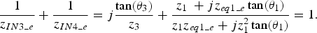 $$\displaystyle{1 \over {z_{IN3\_e} }}+\displaystyle{1 \over {z_{IN4\_e} }}=j\displaystyle{{\tan \lpar {\theta_3 } \rpar } \over {z_3 }}+\displaystyle{{z_1 \; +jz_{eq1\_e} \tan \lpar {\theta_1 } \rpar } \over {z_1 z_{eq1\_e}+jz_1 ^2 \tan \lpar {\theta_1 } \rpar }}=1. $$
From (5), the real and imaginary parts of the two members of the equation are split in two complex equations. Equation (6) is obtained by equating the real parts, while equation (7) corresponds to the imaginary parts.
 $$\eqalign{&z_{1\; } z_2 ^3 z_3 - 3z_1 ^2 z_2 ^2 z_{3\; } \tan \lpar {\theta_1 } \rpar \tan \lpar {\theta_2 } \rpar +z_1 ^2 z_{3\; } \tan \lpar {\theta_1 } \rpar \tan \lpar {\theta_2 } \rpar ^3 \cr & \quad =- z_1 z_{2\; } z_{3\; } \tan \lpar {\theta_2 } \rpar ^2 - 4z_2 ^2 z_{3\; } \tan \lpar {\theta_1 } \rpar \tan \lpar {\theta_2 } \rpar \; \;\cr & \quad - 4z_{1\; } z_2 ^2 \tan \lpar {\theta_2 } \rpar \tan \lpar {\theta_3 } \rpar - z_1 ^2 z_2 ^3 \tan \lpar {\theta_1 } \rpar \tan \lpar {\theta_3 } \rpar \cr & \quad +3z_1 ^2 z_{2\; } \tan \lpar {\theta_1 } \rpar \tan \lpar {\theta_2 } \rpar ^2 \tan \lpar {\theta_3 } \rpar \comma \; } $$
 $$\eqalign{&z_{1\; } z_2 ^2 z_3 \tan \, \lpar \theta _2 \rpar +z_1 ^2 z_2 ^3 z_{3\; } \tan \, \lpar \theta _1 \rpar - 3z_1 ^2 z_{2\; } z_{3\; } \tan \lpar {\theta_1 } \rpar \hbox{tan} \lpar {\theta_2 } \rpar ^2 \cr & =z_1 z_{3\; } \tan \lpar {\theta_2 } \rpar ^3 +2z_2 ^3 z_{3\; } \tan \, \lpar \theta _1 \rpar - \; 2z_{2\; } z_{3\; } \tan \, \lpar \theta _1 \rpar \tan \lpar {\theta_2 } \rpar ^2\cr & \quad +2z_{1\; } z_2 ^3 \tan \lpar {\theta_3 } \rpar - \; 2z_{1\; } z_{2\; } \tan \lpar {\theta_2 } \rpar ^2 \tan \, \lpar \theta _3 \rpar \cr & \quad - 3z_1 ^2 z_2 ^2 \tan \, \lpar \theta _1 \rpar \tan \, \lpar \theta _2 \rpar \tan \, \lpar \theta _3 \rpar \cr & \quad +z_1 ^2 \tan \, \lpar \theta _1 \rpar \tan \lpar {\theta_2 } \rpar ^3 \tan \, \lpar \theta _3 \rpar .}.$$
Similarly, impedance z IN3_e looking toward TLine (z 3, θ 3) is parallel to port 2 impedance, so that the equivalent impedance named z eq2_e is:
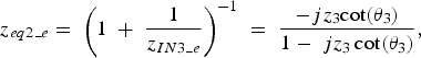 $$z_{eq2\_e}=\; \left({1\; +\; \displaystyle{1 \over {z_{IN3\_e} }}} \right)^{ - 1} \; =\; \displaystyle{{ - jz_3 \hbox{cot}\lpar {\theta_3 } \rpar } \over {1 - \; jz_3 \cot \lpar {\theta_3 } \rpar }}\comma \; $$
z IN1_e is the input impedance of TLine (z 1, θ 1) loaded by z eq2_e, given by (9):
 $$z_{IN1\_e}=\; z_1 \displaystyle{{z_{eq2\_e} \; +jz_1 \tan \lpar {\theta_1 } \rpar } \over {z_1+jz_{eq2\_e} \tan \lpar {\theta_1 } \rpar }}. $$
The combination of z IN1_e parallel to z IN2_e should be equal to port 1 impedance to obtain a matching condition at port 1, leading to equation (10):
 $$\eqalign{\displaystyle{1 \over {z_{IN1_{\_e} } }}+\displaystyle{1 \over {z_{IN2\_e } }} & =\displaystyle{{z_1 \; +\; jz_{eq2\_e} \tan \lpar {\theta_1 } \rpar } \over {z_1 z_{eq2\_e}+jz_1 ^2 \tan \lpar {\theta_1 } \rpar }}+j\displaystyle{{\tan \lpar {\theta_2 } \rpar } \over {2z_2 }} \cr & \quad = \displaystyle{1 \over 2}.} $$
By developing and equating the real and imaginary parts of the two members of equation (10), equations (11) and (12) are derived:
 $$\eqalign{& z_{1\; } z_3 \tan \lpar {\theta_2 } \rpar \cot \lpar {\theta_3 } \rpar - z_1 ^2 \tan \lpar {\theta_1 } \rpar \tan \lpar {\theta_2 } \rpar \cr & +2z_1 z_2+2z_2 z_3 \tan \lpar {\theta_1 } \rpar \cot \lpar {\theta_3 } \rpar =\; z_1 ^2 z_{2\; } z_{3\; } \tan \lpar {\theta_1 } \rpar \cot \lpar {\theta_3 } \rpar \comma \; } $$
 $$\eqalign{& z_{1\; } z_3 \tan \lpar {\theta_1 } \rpar \tan \lpar {\theta_2 } \rpar \cot \lpar {\theta_3 } \rpar - \; z_2 z_3 \cot \lpar {\theta_3 } \rpar \cr & \quad =\; z_1 z_2 \tan \lpar {\theta_1 } \rpar }. $$
Finally, the even-mode analysis leads to four different equations, (6), (7), (11), and (12).
B) Odd-mode analysis
For the odd-mode analysis, the voltages at ports 2 and 3 have the same magnitude and are 180° out of phase. The voltage is consequently null along the plane of symmetry of the circuit which can be thus short circuited in its middle part. The impedance looking toward the circuit from port 2 can be calculated through the impedances z IN3_o and z IN4_o:
 $${z_{IN3\_o}} = {z_3} {\displaystyle{{r \big/ 2} + j{z_3}\tan \lpar {\theta _3}\rpar } \over {{z_3} + j{r \big/ 2}}\tan \lpar {\theta _3}\rpar }\comma $$
 $$z_{IN4\_o}=jz_1 \tan \lpar {\theta_1 } \rpar . $$
The combination of these two parallel impedances should match port 2 impedance, which leads to the following equation (15):
 $$\eqalignno{&\displaystyle{1 \over {z_{IN3\_o} }}+\displaystyle{1 \over {z_{IN4\_o} }}=\displaystyle{{z_3 \; +\; j\lpar r/2\rpar \tan \lpar {\theta_3 } \rpar } \over {z_3 \lpar r/2\rpar \; +\; jz_3 ^2 \tan \lpar {\theta_3 } \rpar }} - \; j\displaystyle{{\cot \lpar {\theta_1 } \rpar } \over {z_1 }}=1.}$$
Equations (16) and (17) are obtained by equating the real and imaginary parts of equation (15), respectively:
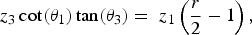 $$z_3 \cot \lpar \theta _1 \rpar \tan \lpar {\theta_3 } \rpar =\; z_1 \left({\displaystyle{r \over 2} - 1} \right)\comma \; $$
 $$- z_3 \cot \lpar \theta _1 \rpar \cot \lpar \theta _3 \rpar =z_1 \left({\displaystyle{2 \over r}z_3^2 - 1} \right). $$
Next, equation (16) is substituted into (17) in order to get:
 $$\theta _3=\; \tan ^{ - 1} \left({\sqrt {\displaystyle{{ - \lpar r/2\rpar \; \; +\; \; 1} \over {\; \lpar 2z_3^2 /r\rpar \; - \; \; 1}}} } \right)\comma \; $$
which implies the following condition on r according to z 3:
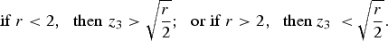 $$\hbox{if}\, \, r\lt 2\comma \; \, \, \hbox{then}\, \, z_3\gt \sqrt {\displaystyle{r \over 2}}\semicolon \; \, \, \hbox{or if}\, \, r\gt 2\comma \; \, \, \hbox{then }z_{3\; }\lt \sqrt {\displaystyle{r \over 2}} . $$
What is more, equation (16) can be rewritten as follows:
 $$\theta _1=\; \tan ^{ - 1} \left({\displaystyle{{z_3 \tan \lpar \theta_3 \rpar } \over {z_1 \lpar {\; \lpar r/2\rpar - 1} \rpar }}} \right). $$
From equation (20), it is obvious that the value of r cannot be lower than 2, which would lead to a negative value of the electrical length θ 1 or an electrical length longer than a quarter wavelengths which is not acceptable. Thus, the right condition among the two suggested in equation (19) is:
 $$r\gt 2\, \, \hbox{with}\, \, z_{3\; }\lt \sqrt {\displaystyle{r \over 2}} . $$
Meanwhile equation (12) can also be rewritten as follows:
 $$\theta _2=\; \tan ^{ - 1} \left({\displaystyle{{z_2 } \over {z_3 \cot \lpar \theta_3 \rpar }}\; +\; \displaystyle{{z_2 } \over {z_1 \tan \lpar \theta_1 \rpar }}} \right). $$
C) Theory and design equations summary
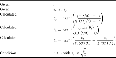
It is remarkable that equation (18) gives θ 3 versus r and z 3 only, equation (20) gives θ 1 versus r, z 1, z 3, and θ 3, and equation (22) gives θ 2 versus z 1, z 2, z 3, θ 1, and θ 3. Table 1 summarizes the theoretical description to calculate easily the length parameters of the three TLines as a function of initial parameters.
III. DESIGN PROCEDURE
With an adequate procedure, it seems possible to find, in that order, the TLines electrical lengths θ 3, θ 1, and θ 2 which solely depend on z 1, z 2, z 3, and r. A set of solutions consists in a fixed r and the three values z 1, z 2, and z 3. For a given r, the exact solution of the six equations, (6–7), (11–12), and (16–17) is reached in the particular case θ 2 = 0, i.e. without open stub. This case is already known and does not lead to miniaturization. More precisely, those six equations were obtained by considering perfect matching on port 1 for the even mode (S 11_e = 0) and perfect matching on port 2 for both even and odd modes (S 22_e = 0) and (S 22_o = 0). In the Appendix, we show that this is equivalent to having a perfect matching on port 2 only (S 22 = 0). We show as well that considering (S 22 = 0) is equivalent to have both matching at all ports and perfect isolation. Consequently a close solution corresponds to S 22 as close to 0 as possible. Meeting the criterion |S 22| <S 22_max means that the initial set of z 1, z 2, and z 3 corresponds to valid characteristic impedances for a compromise solution within the defined limits.
Hence, even if a perfect set of characteristic impedances cannot be found, there are some sets that enable to go as close as possible to the ideal solution, depending on S 22_max. Equations (6), (7), and (11) are too complex to be solved in an algebraic way with equations (18), (20), and (22), so that only the three last are used. The “approximate solutions” can be obtained thanks to the use of a simple algorithm. It consists in calculating S 22 and to compare it with S 22_max, to be fixed as low as possible. On the basis of the demonstration in the Appendix, |S 22| < S 22_max means that S 22 is as close to zero as possible which implies that S 11 and S 23 are also close to 0. The maximum values that |S 11| or |S 23| can reach are not easy to express as a function of S 22_max since they will depend on both real and imaginary parts of S 22 but the tendencies are the same: being close to 0.
It is easy to derive S 22 from Fig. 2. S 22 is the sum of S 22_e for the even mode and S 22_o for the odd mode. S 22_e and S 22_o were calculated on the basis of the equivalent admittances looking toward the circuit from port 2. Equation (23) summarizes the relationship between S 22 and the other parameters.
 $$\eqalign{S_{22} & = S_{22\_e}+S_{22\_o} \cr & =\displaystyle{{z_{IN3\_e}+z_{IN4\_e} - 1} \over {z_{IN3\_e}+z_{IN4\_e}+1}}+\displaystyle{{z_{IN3\_o}+z_{IN4\_o} - 1} \over {z_{IN3\_o}+z_{IN4\_o}+1}}\comma \;}$$
z IN3_e, z IN4_e, z IN3_o, and z IN4_o are related to the isolation resistance (r) and the six parameters of the TLines (z i, θi) by equations (2), (4), (13), and (14), respectively.
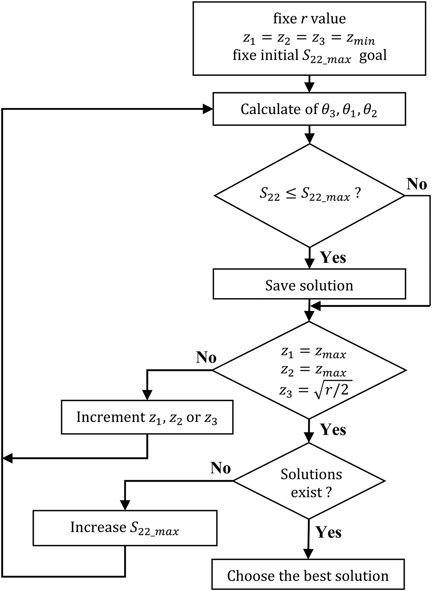
In practice, the algorithm described in Fig. 3 is used to find close solutions, only based on the port 2 matching condition. This algorithm is implemented on Matlab with the help of the RF toolbox.
Fig. 3. Algorithm to find solutions.
First, r must be fixed to the desired value and z 1, z 2, and z 3 to the minimum achievable characteristic impedance given by the technology. Included in the three overlapping loops of z 1, z 2, and z 3 (symbolized with only one block in the algorithm), the three electrical lengths θ 3, θ 1, and θ 2 are calculated in this order, according to equations (18), (20), and (22). Then S 22 is compared with the initial condition. Typically, it is a good choice to start the procedure with S 22_max = −35 dB. If after any combinations of z 1, z 2, and z 3, S 22 stays higher than S 22_max, this means that the goal is not achievable. Consequently, S 22_max should be slightly increased. The softer the conditions concerning S 22_max is, the worse the isolation and matching of the PD are. In practice, the choice of S 22_max is deserved to the designer, depending on the specifications related to the application.
Finally, additional conditions concerning θ i and/or z i ranges, may have consequences on the device maximum size and on the quality factor of the TLines (in particular if integrated technologies are targeted). The designer thus can choose a compromise between the PD electrical performance and its size by electing the appropriate values of the characteristic impedances and electrical lengths, as in [Reference Zhao, Long and Spirito11].
IV. CIRCUITS DESIGN AND EXPERIMENTAL RESULTS
As shown in (21), r should be strictly bigger than the normalized value 2, i.e. R > 100 Ω when considering a 50-Ω system characteristic impedance. In this paper, two PDs with two different values of R were fabricated to illustrate and validate the method described in Section III, one with R = 105 Ω and one with R = 150 Ω, respectively. Upper case letters used to describe the experimental characteristic impedances or resistances are related to the lower case ones of the theory by means of the system impedance Z 0 = 50 Ω.
A) PD with R = 105 Ω
The condition for S 22 was fixed to −35 dB. The characteristic impedances range of variation was fixed to (25 Ω; 100 Ω), except for Z 3 which is limited to 51 Ω from (21). A step of 2 Ω is a good compromise between time simulation and impedance resolution for the outline of the design graphs. . Once all the possible sets of impedances, Z 1, Z 2, and Z 3 in their respected range, have been explored, the process ends with various solution sets that fit the condition on S 22. Figure. 4 is an easy way of representation of the solutions. It also enables to plot the various electrical lengths corresponding to the solutions sets. As θ 3 only depends on Z 3, it has been plotted alone in Fig. 4(a). This map shows that the higher Z 3 is, the longer θ 3 is. It also shows that any value of Z 3 within its variation range is part of a solution set. Fig. 4(b) focuses on Z 1 and θ 1. For each possible value of Z 3, two, three, or four Z 1 may be part of a solution set. As θ 1 only depends on Z 3 and Z 1, it can be thus calculated and represented in color scale on the same graph. It is interesting to point out that the higher Z 1 is and the shorter θ 1 is. Finally, Fig 4(c) focuses on stub (Z 2, θ 2). It can be seen that for any couple (Z 1, Z 3) that is part of a solution set, all the values of Z 2 in the range [25 Ω; 100 Ω] may fit the criterion S 22 < S 22_max. It is noticeable that shorter stub length, θ 2, is required when Z 2 lowers.
Fig. 4. Design graphs for R = 105 Ω.
Hence, there exists a large number of solutions sets that fit the criterion on S 22. Depending on the objective — strongly miniaturized PD or the specific shape for antennas array — the designer may choose one set or another. Our solution thus leads to high flexibility in the design, which is its major interest while maintaining good electrical performances.
In the present example, a strong miniaturization is required. It could be reached with the choice of Z 3 = 25 Ω and θ 3 = 14.4°. With such solution, several values for Z 1 and θ 1 are then available. Z 1 = 81 Ω appears to be a good compromise to avoid too high characteristic impedances, which leads to θ 1 = 57.7°. Lastly, Fig. 4(c) gives the electrical length θ 2 versus Z 1 and Z 2, for various achievable values of Z 3. Many possibilities exist for the pair (Z 2, θ 2). Based on Z 3 = 25 Ω and Z 1 = 81 Ω, a wide range remains possible. Design constraints can be taken into account for the choice of the pair (Z 2, θ 2). In particular, θ 2 should be chosen short enough to avoid parasitic coupling between the TLines (Z 1, θ 1) and (Z 2, θ 2). Z 2 = 39 Ω, leading to θ 2 = 35.2°, were chosen in the present design.
The circuits were fabricated on the dielectric substrate Rogers RO4003C™, of relative dielectric constant 3.38 and thickness 813 µm. All circuits are working at the frequency of 2.45 GHz. A SOLT calibration was carried out on an 8720 Vector Network Analyzer. The resistance R was measured equal to 100.2 Ω, 5% lower than the expected value of 105 Ω. Figure. 5 compares the S-parameters obtained from electromagnetic (EM) simulations on ADS-Momentum (with R = 105 Ω, as in the design procedure) and measurements (with R = 100.2 Ω, respectively). Despite the lower value of R, a very good agreement is obtained.
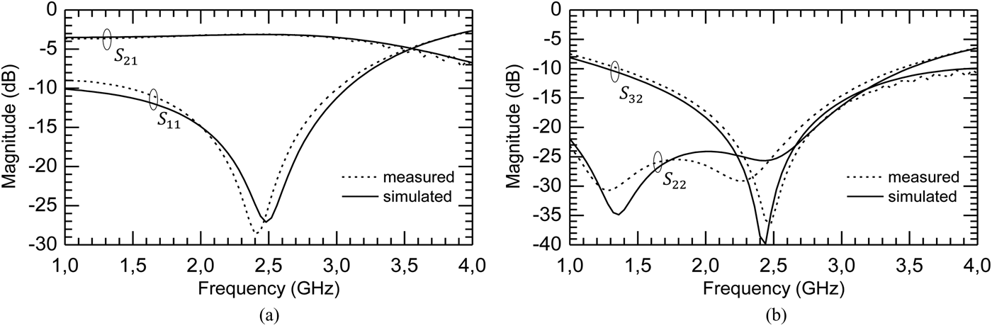
Fig. 5. Simulation and measurement results of the proposed topology with R = 105 Ω in EM simulations, R = 100.2 Ω for measurements, 5% smaller than expected. (Z 1, θ 1) = (81 Ω, 57.7°), (Z 2, θ 2) = (39 Ω, 35.2°), (Z 3, θ 3) = (25 Ω, 14.4°). (a) Insertion loss and input return loss. (b) Isolation and output return loss.
As expected the PD is very low loss with 0.13 dB of insertion loss only at 2.45 GHz, partially due to SMA RF connectors. The available bandwidth, defined by S 11 below −15 dB, reaches 34%, from 2 to 2.84 GHz. Considering this bandwidth, the output port return loss S 22 and the isolation S 23 are better than −17 and −18 dB, respectively. They reach −26 and −34 dB at 2.45 GHz, respectively. Remember that S 22 was fixed to −35 dB as an input condition of the design algorithm. Even if −35 dB is reached in the design process on Matlab, calculi are based on theoretical equations only and do not take into account junctions' electrical models nor parasitic couplings that in practice contribute to degrade the return loss. Moreover, the value of R was 5% below the targeted value, which also explains the discrepancy between −35 and −26 dB at 2.45 GHz. It is worth emphasizing that −26 dB as a measured return loss provides excellent matching conditions for a large majority of applications.
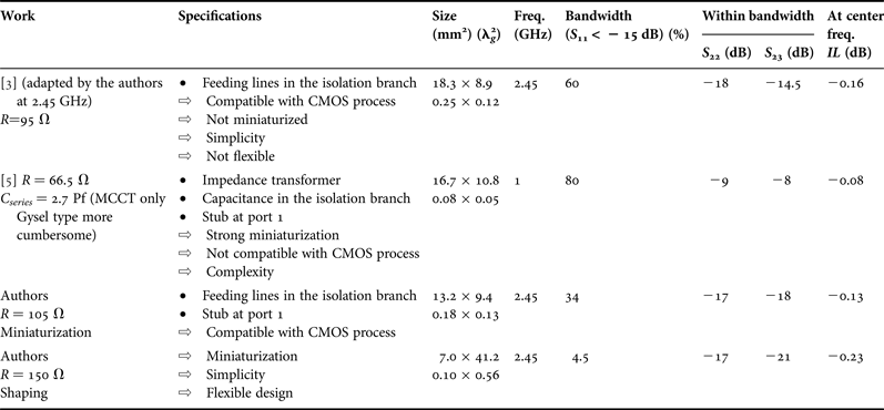
Figure 6 is a viewgraph of the fabricated PD compared with the modified PD early proposed in [Reference Horst, Bairavasubramanian, Tentzeris and Papapolymerou3] and re-designed by the authors for valuable comparison. To design the latter, the value of R was fixed to 95 Ω to get an electrical length of the TLines equal to 12.6° between the output ports and the resistance, which is close to the 14.4° chosen for the topology presented here. The TLines characteristic impedance was fixed to 69 Ω, with an electrical length between ports 1 and 2 (or 3) equal to 102.6°. These values lead to a surface of the herein proposed circuit that is 24% smaller compared with that proposed in [Reference Horst, Bairavasubramanian, Tentzeris and Papapolymerou3]. Scattering parameters are summarized in Table 2.
Fig. 6. Measured circuits. (a) Proposed design. (b) Modified PD from [3].
Table 2. Pros and cons comparison with previous works.
To conclude, these results suggest that the proposed PD is low loss, with really good matching and isolation. It is smaller and more flexible than the one proposed in [Reference Horst, Bairavasubramanian, Tentzeris and Papapolymerou3] while keeping similar advantages such as the limitation of the parasitic coupling between the output ports thanks to the TLines connecting the resistance. In terms of simplicity, miniaturization, and performance, this design is also clearly well suited to further circuit integration considerations.
B) PD with R = 150 Ω for antenna array feeding circuits
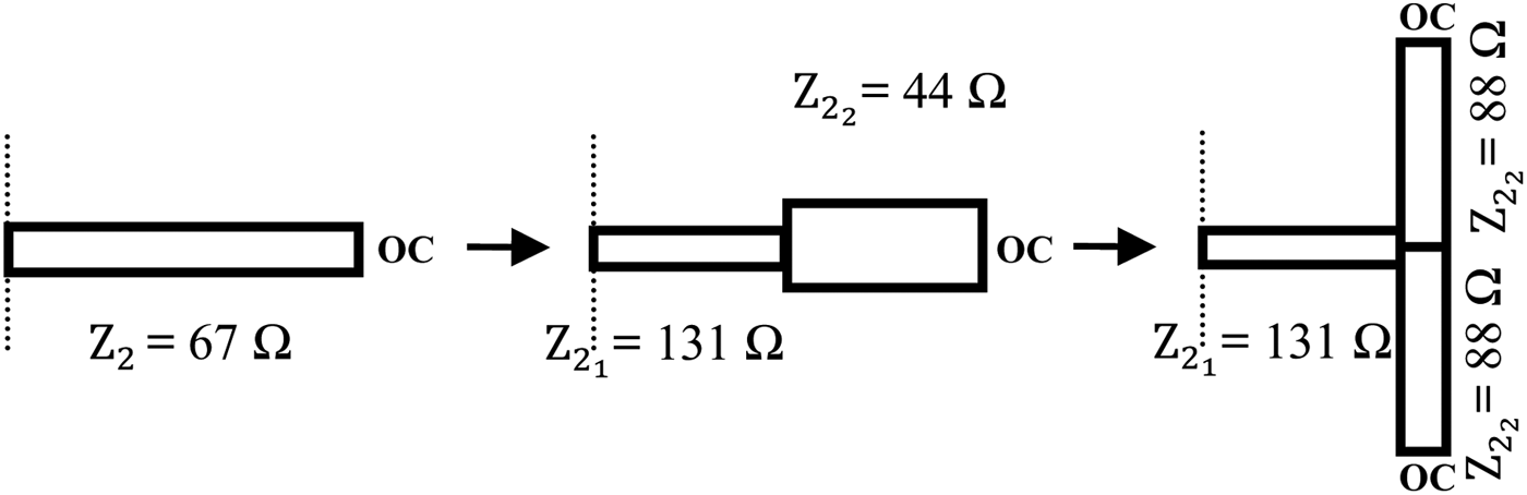
Another PD was achieved and measured with R fixed to 150 Ω. As for the previous one the maximum value of S 22 was fixed to −35 dB for the initial design, the characteristic impedances still varied between 25 and 100 Ω, and Z 3 was limited to 61 Ω. Following a design graphs procedure as the one proposed in Fig. 4, it is shown that the solution θ 3 = 49°, Z 3 = 49 Ω, θ 1 = 60°, and Z 1 = 65 Ω enables high flexibility in terms of PD shape with a relatively long TLine connecting the output ports to the resistance. In the counterpart, particular attention was paid on the electrical length θ 1 that should be longer than θ 3 to avoid meandering of the TLine (Z 3, θ 3). The open-circuit stub (Z 2, θ 2) was designed in a T shape to fit the free space in the PD loop. To get more flexibility and reduce the length of the stub, the TLine (Z 2 = 67 Ω and θ 2 = 66°) was realized by a stepped-impedance structure, as shown in Fig. 7, with Z 21 = 131 Ω, θ 21 = 6.2°, Z 22 = 44 Ω, and θ 22 = 41°, respectively. Z 21 can be considered as a high characteristic impedance, but such a value is still achievable in a classical PCB technology. Its shortness should not bring too much loss. Finally, the TLine with the lower characteristic impedance was divided in two parallel TLines of similar electrical length but with characteristic impedance multiplied by 2, so that Z 22 becomes now equal to 88 Ω.
Fig. 7. Steps to design the open stub (Z 2, θ 2) to fit the free space in the PD (not to scale).
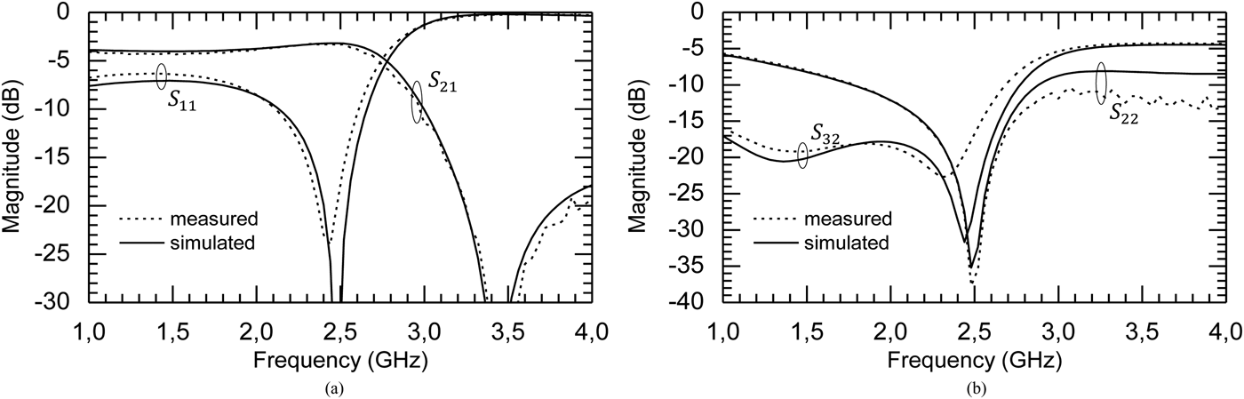
Figure 8 compares the S-parameters obtained from EM simulations on ADS-Momentum and measurements. Here again, the agreement between simulation and measurement results is very good. The insertion loss is 0.23 dB at 2.45 GHz and the bandwidth reaches 4.5%, from 2.37 to 2.48 GHz (Fig. 8(a)). The return loss at the output port S 22 is better than −17 dB and the isolation S 32 is better than −21 dB in the defined bandwidth. They reach −19 and −29 dB at 2.45 GHz, respectively (Fig. 8(b)). This PD is only slightly smaller (6%) than the one presented in [Reference Horst, Bairavasubramanian, Tentzeris and Papapolymerou3]. But its topology proves a huge shape flexibility which can, by the end, save much space in a global system. Here, the cost of such flexibility is a reduced bandwidth.
Fig. 8. Simulation and measurement results of the proposed topology with R = 150 Ω. (Z 1, θ 1) = (65 Ω, 60°), (Z 21, θ 21) = (131 Ω, 6.2°), (Z 22, θ 22) = (88 Ω, 41°), (Z 3, θ 3) = (49 Ω, 49°). (a) Insertion loss and input return loss. (b) Isolation and output return loss.
A utilization of the fabricated PD is illustrated in the next section where a 4-antennas feeding circuit was realized as a proof of concept.
C) Antennas array feeding circuit
The PD of Section IV.B was used in a 1:4 feeding circuit of an antennas array. Figure. 9 shows the fabricated feeding circuit. Two PDs were connected in parallel at the outputs of a first one by means of TLines, called (Z 4, θ 4), in such a way that each output stays equidistant from its neighbors (see Fig. 9). Z 4 and θ 4 were fixed after a tuning procedure. The choice of characteristic impedance Z 4 different from 50 Ω offers the opportunity to slightly increase the feeding circuit bandwidth as compared with a single power divider. Z 4 and θ 4 were taken equal to 45 Ω and 165°, respectively.
Fig. 9. 1:4 feeding circuit.
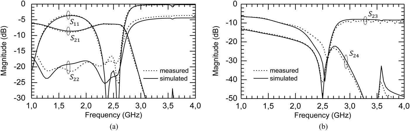
Figure 10 shows the comparison between the simulation and measurement results. The agreement is very good. The insertion loss is 0.48 dB below the ideal value of 6 dB at 2.45 GHz. The bandwidth, defined by S 11 below −15 dB, reaches 15% (Fig. 10(a)). In the considered bandwidth, the return loss at the output port S 22 is better than −15 dB. The isolation S 23, which is the one between two outputs of the same PD (i.e. between output ports 2 and 3, or 4 and 5, respectively) is better than −15 dB, while the isolation S 24 which is the one between two outputs from different PDs is better than −23 dB (Fig. 10(b)). At 2.45 GHz, S 11, S 22, S 23, and S 24 are equal to −17, −18, −21, and −35 dB, respectively. It would be very easy to improve the network return loss thanks to the tuning of the TLines (Z 4, θ 4). This would lead, in counterpart, to the reduction of the bandwidth.
Fig. 10. Simulation and measurement results of the 1:4 feeding circuit. (a) Magnitude of S 21, S 11, and S 22. (b) Magnitude of S 23 and S 24.
Thanks to the particular shape of the proposed circuit, it is possible to save more surface area compared with what could be obtained with more conventional Wilkinson-type PDs.
V. COMPARISON WITH PREVIOUS WORKS
As aforementioned, compared with [Reference Horst, Bairavasubramanian, Tentzeris and Papapolymerou3], the PD with 105 Ω enables to save space (24%), while maintaining similar or better electrical performances. Bandwidth is lower but the 60% bandwidth in [Reference Horst, Bairavasubramanian, Tentzeris and Papapolymerou3] is unnecessary in most cases, for RX systems are already limited by the power amplifiers bandwidth. The PD realized in this paper is also compatible with a CMOS process. The PD with 150 Ω claims the same advantages with a bigger surface. It has been shaped to save space once assembled in a 1:4 feeding circuit for antenna arrays. It is a very low bandwidth but it was demonstrated that bandwidth could be extended up to 15% when inserted in a 1:4 antenna array feeding network. Compared with [Reference Ahn5], the proposed solution with 105 Ω is less miniaturized. However, [Reference Ahn5] would need big changes in terms of re-design for CMOS compatibility. By imagining that feeding lines are considered in the isolation branch and that the overall re-design stays as much miniaturized in terms of λ gReference Pozar2, the connection to a Metal–Insulator–Metal capacitance will be necessary. The added surface due to the capacitance would finally lead to less miniaturization. In [Reference Ahn5], matching at port 2 and isolation between ports 2 and 3 are poor as compared with the proposed PD. This is due to the trade-off between an extremely large bandwidth and the return loss.
VI. CONCLUSION
This paper was focused on the design and fabrication of PDs working at RF frequencies and was carried out in a classical PCB technology. The design consists in a modified Wilkinson power divider. It takes into account the output isolation resistance feeding TLines used to avoid coupling between the output ports. It also associates an open stub at the input port junction. While keeping very good isolation between output ports and matching on all ports, the proposed PD enables an optimal choice of the characteristic impedance of the transmission lines, flexibility in the output ports position, and size reduction. The PD is really easy to design, with no reactive lumped element. Depending on the considered technology, the best compromise may be chosen between size and electrical performance. Design rules were given thanks to design graphs, and a simple method consisting in searching sets of solutions was described. The design method is valid at center frequency; further circuit analysis is then required to explore the entire targeted frequency band.
Two PDs were realized for a proof-of-concept, with different characteristics, to show the potentiality for miniaturization or flexibility in the choice of the output ports position. Measurement and simulation results were in very good agreement. Then, a 1:4 antenna array feeding network was achieved. Thanks to the PD flexibility, the surface area of this feeding network was minimized. Here again, measurement and simulation results were in very good agreement.
This study confirms that the new proposed topology is well suited for CMOS millimeter-wave technologies. First, the considered characteristic impedances are achievable in a CMOS process, together with the isolation resistances values. Then, in order to fit the topology of the device placed just after PD, spacing between ports 2 and 3 can be specified as an initial condition. Using the proposed design process, a miniaturized solution may be found, which is of major importance in CMOS for cost reasons. Finally, the design can be very simple, with straight horizontal, vertical, or 45° only connection lines which is mandatory in CMOS design rules.
ACKNOWLEDGEMENTS
The research leading to these results has been conducted in the frame of the European ENIAC MIRANDELA project and it received funding from the ENIAC Joint Undertaking under grant agreement number 120221 together with funding from the French Direction Générale de la Compétitivité, de l'Industrie et des Services under convention N°102930164.
APPENDIX
This appendix aims at demonstrating that a matching condition on the scattering parameter S 22 of a PD is enough to ensure good isolation and input matching. Statement is valuable for any three-port network as long as (i) the symmetry condition between ports 2 and 3 is verified (balanced network) and (ii) there is no loss in the equivalent even-mode circuit (which means no resistive element in the even-mode circuit). Those conditions are fulfilled by the PD represented in Fig. 1(c). Due to condition (i) the later can be redrawn as the four ports network in Fig 11(a).
Fig. 11. (a) Normalized representation of Fig. 1(c) as a four ports network, (b) odd-mode, and (c) even-mode schematics.
Based on those considerations, the network can be analyzed by an even/odd-mode approach. Naming a 1, the input power wave at port 1, the following equations hold for the relationships between the power waves defined in Fig. 11:
 $$\matrix{{a_1^{\prime} = a_{1\_e}^{\prime} + a_{1\_o}^{\prime} \comma \; } & {b_1^{\prime} = b_{1\_e}^{\prime} + b_{1\_o}^{\prime} \comma \; } \cr {{a}_1^{{\prime}{\prime}} = a_{1\_e}^{\prime} + a_{1\_o}^{\prime} \comma \; } & {b_1^{\prime} = b_{1\_e}^{\prime} - b_{1\_o}^{\prime} \comma \; } \cr {{a_1} = {a_{1\_e}} + {a_{1\_o}} \comma \; } & \!{{b_1} = {b_{1\_e}} + {b_{1\_o}}.} \cr }$$
In the same manner, if an input power wave a 2 is considered at port 2, or a 3 at port 3, the following equations occur:
 $$\matrix{ {a_2=a_{2\_e}+a_{2\_o}\comma \; } & {b_2=b_{2\_e}+b_{2\_o}\comma \; } \cr {a_3=a_{2\_e} - a_{2\_o}\comma \; } & {b_3=b_{2\_e} - b_{2\_o} .} \cr }$$
A. ODD-MODE ANALYSIS
As port 1 is shunted (Fig. 11,b), no transmission may occur between ports 1 and 2. Consequently, the general form of the odd-mode reciprocal scattering matrix [S o] is written as:
 $$\left[{\matrix{ {S_{11\_o} } & 0 \cr 0 & {S_{22\_o} } \cr } } \right].$$
From Fig. 11(b), we get a 1_o′ = −b 1_o′, which can be stated as |S 11_o| = 1. With the presence of a resistance in the network, the matrix cannot be unitary. Necessarily |S 11_o| ≠ |S 22_o| and |S 22_o| ≠ 1.
Moreover, as a 1_o = a 1_o′ − a 1_o′, and b 1_o = b 1_o′ −b 1_o′, power waves a 1_o and b 1_o may be expressed in the odd mode as:
 $$a_{1\_o}=0\comma \; \quad b_{1\_o}=0.$$
B. EVEN-MODE ANALYSIS
The even-mode scattering reciprocal matrix [S e] takes the form below:
 $$\left[{\matrix{ {S_{11\_e} } & {S_{12\_e} } \cr {S_{12\_e} } & {S_{22\_e} } \cr } } \right].$$
The even-mode network being lossless, the even matrix is unitary and the two following equations held:
 $$S_{11\_e}^2+S_{12\_e}^2=1\quad \hbox{and}\quad \vert {S_{22\_e} } \vert =\vert {S_{11\_e} } \vert.$$
Moreover, in Fig. 11(a), at port 1, half power comes from the upper port 1′ and half from the lower port 1″, so that power waves a 1_e and b 1_e may be expressed as:
 $$a_{1\_e}=\sqrt 2 \cdot a^{\prime}_{1\_e}\comma \; \quad b_{1\_e}=\sqrt 2 \cdot b^{\prime}_{1\_e}.$$
C. DISCUSSION ON THE SCATTERING PARAMETERS
Equations (24), (25), (27), and (30) give a relationship between even, odd, and global power waves. It is thus possible to link one to each other the parameters of the three-port matrix [S] with the parameters of the two-port matrices [S o] and [S e]:
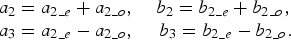
 $$\eqalign{& S_{11}=S_{11\_e}\comma \; \cr & S_{12}=\displaystyle{{S_{12\_e} } \over {\sqrt 2 }}=S_{13}=S_{21}=S_{31}\comma \; \cr & S_{22}=S_{22\_e}+S_{22\_o}=S_{33}\comma \; \cr & S_{23}=S_{22\_e} - S_{22\_o}=S_{32} .}$$
To design a three-port device, a parametric study is often necessary. A defined limit of the design process may consist in conditions on the scattering parameters. Various possibilities can be enforced.
C.1 Condition |S 11| = 0
This condition leads to |S 11_e| = 0, implying |S 12_e| = 1, and hence  $S_{12}=1/\sqrt 2 $.
This is sufficient as long as output ports matching is not required. However, such a condition is not enough for the use of a PD as a combiner where isolation is required.
C.2 Condition |S 22| = 0
Two solutions exist. The first one consists in equating S 22_e to −S 22_o which is undoubtedly meaningless. The second one is equivalent to having at the same time matching for both even- and odd-modes at port 2:
 $$S_{22\_o}=S_{22\_e}=0.$$
Consequently:
• Matching on port 1 is realized:
Considering (29), S 22_e = 0 implies:
 $$S_{11\_e}=0.$$
Considering (31), S 11_e = 0 implies:
 $$S_{11}=0.$$
• − 3 dB ratio between ports 1 and 2 is reached:
Considering (29), S 11_e = 0 implies:
 $$S_{12\_{\rm e}}=1.$$
Considering (31), S 12_e = 1 implies:
 $$S_{12}=1/\sqrt 2.$$
• Perfect isolation is realized:
Considering (31), S 22_o = S 22_e = 0 implies:
 $$S_{23} = 0.$$
D. CONCLUSION
A matching condition on the scattering parameter S 22 alone holds for the four conditions on S 22, S 11, S 12, and S 23 as long as the PD stands symmetrical and lossless (except the isolation resistance R).
In practice, having |S 22| = 0 may be impossible. Assuming, as a criterion to meet, that |S 22| < S 22_max, or in other words, trying to have S 22 close to 0, implies S 22_e close to 0 too, which is equivalent to S 11 = S 11_e = S 22_e close to 0 as well. The maximum value that |S 11| will reach is not easy to express as a function of S 22_max as it will depend on both real and imaginary parts of S 22 but the tendency is the same: being close to 0. The argumentation is similar for S 23.
François Burdin received his M.Sc. degree in Electrical Engineering in 2010 and his Ph.D. degree at the “INstitut Polytechnique de Grenoble” (G-INP), University of Grenoble-Alpes, France, in 2013. In 2013, he joined the Chassis Systems Control division of Robert Bosch GmbH in Budapest, Hungary. His main work concerns the antennas and the high-frequency PCB of the radars sensors, as well as the vehicle integration topic for the radars.
Florence Podevin received her M.Sc. degree in Electronics and Microelectronics Engineering from the Université des Sciences et Technologies de Lille (USTL), in 1998 and her Ph.D. degree in Microelectronics from the USTL, in 2001. In 2001, she joined the Institute of Microelectronics Electromagnetism and Photonic (IMEP-IMEP-LAHC) in Grenoble as an assistant Professor. Her main research concerns passive devices for millimeter waves based on slow-wave transmission lines, tunable or not, in CMOS or beyond CMOS nanotechnologies. She authored or co-authored almost 45 papers published in international journals or conferences and co-holds one patent.
Philippe Ferrari received his M.Sc. degree in Electrical Engineering in 1989 and his Ph.D. degree from the “Institut National Polytechnique de Grenoble” (INPG), France, in 1992.
In 1992, he joined the laboratory of microwaves and characterization of the University of Savoy, France, as an assistant Professor in electrical engineering, and was involved in the development of RF characterization techniques. From 1998 to 2004, he was the head of the laboratory project on non-linear transmission lines and tunable devices. Since 2004, he is a Professor at the Grenoble-Alpes University, France, and he continues his research at the Institute of Microelectronics Electromagnetism and Photonic (IMEP, IMEP-LAHC since 2007). He is the head of the RF and Millimeter-wave group (RFM). His main research interest concerns tunable and miniaturized devices, such as filters, phase shifters, matching networks, and power dividers, and new circuits based on slow-wave transmission lines, at millimeter-wave frequencies, in CMOS and BiCMOS technologies. He is author or co-author of more than 150 papers published in international journals or conferences, and co-holder of five patents. He is an IEEE senior member, a member of the Editorial Board of the International Journal on RF and Microwave Computer-Aided Engineering (Wiley), and an Associate Editor of the International Journal of Microwave and Wireless Technologies (EuMA). He is also a TPC member of the European Microwave Conference and the French microwave Conference.