I. INTRODUCTION
Nowadays, W-band (around 80 GHz) is widely used all over the world for several applications, such as automotive radar [1, 2], high-speed networks [3], imaging, and gesture recognition [Reference Arbabian, Callender, Kang, Rangwala and Niknejad4]. In 2009, European Telecommunication Commission Institute (ETSI) has assigned a short range radar band from 77 to 81 GHz [1]. In 2012, the International Telecommunication Union (ITU) has recommended vehicular collision avoidance radars in the frequency band from 77 to 81 GHz [2] and fixed wireless systems operating in the 71–76 and 81–86 GHz range [3]. A 94 GHz pulsed-radar transceiver was reported for the applications of imaging and gesture recognition [Reference Arbabian, Callender, Kang, Rangwala and Niknejad4].
Mixer is a key component of the radiofrequency (RF) transceivers. For W-band receivers, sub-harmonic mixer (SHM) is an attractive solution since it mixes the RF signal with the second harmonic of LO (2*f LO ) signal. With relatively low oscillation frequency, the oscillator has better phase noise performance, and the buffer of the oscillator can provide higher LO power with lower power consumption [Reference Hung, Hancock and Rebeiz5].
Since the passive SHMs have significant conversion loss, there are many topologies reported to implement active SHMs with conversion gain. Paper [Reference Hung, Hancock and Rebeiz5] reported an SHM topology with a compact input network, which transfers RF signals from single-ended to differential while keeping LO signals in phase at the base of the differential transistors. This topology has high LO–RF and 2LO–RF isolation between the LO and RF ports. However, it is challenging to realize the RF and LO input matching at the same time. Thus, this topology requires high LO pumping power.
Gilbert-cell SHMs with three-level stacked-LO switching core [Reference Sheng, Jensen and Larson6–Reference Zhao, Öjefors, Aufinger, Meister and Pfeiffer9] are widely used, which use the current switching mechanism to generate 2*f LO signal for mixing. Other Gilbert-cell leveled-LO SHM topologies were reported including both bottom-LO configuration [Reference Zhang, Chen, Tsui and Lau10–Reference Syu, Meng and Wang12] and top-LO configuration [Reference Fang, Lee, Allstot and Bellaouar13–Reference Tsai, Yang, Huang and Wang15], which use the nonlinearities of transistors to generate 2*f LO signal for mixing. The design trade-offs of the Gilbert-cell SHMs between stacked-LO and leveled-LO configurations were reported in [Reference Wu, Tseng, Meng and Huang16]. It is reported that Gilbert-cell stacked-LO SHM has lower LO power requirement but lower operational frequency than the Gilbert-cell leveled-LO SHMs. This trade-off is mainly caused by the different operational principles. The transistor switching characteristic used by stacked-LO SHM is sensitive to signal frequency. The transistor nonlinearities used by leveled-LO SHMs is sensitive to signal power. In addition, all these Gilbert-cell SHM topologies require a precise quadrature LO signal and have complicated circuit layouts.
The common emitter common collector transistor pair (CECCTP) SHMs with top-LO-configuration were also reported in [Reference Maeda, Taniguchi, Ono, Suematsu and Takagi17, Reference Wang18]. Owing to differential LO signal input and simple circuit layout, CECCTP structure is considerable for millimeter-wave SHM IC. In the conventional top-LO-configured CECCTP SHM, however, the bottom RF stage suppresses the generation of 2*f LO signal and results in a high requirement of LO power. Hence, we propose an improved bottom-LO-configured CECCTP SHM IC with a tail current source for W-band applications [Reference Yang, Xu, Zheng, Shibata and Yoshimasu19]. The improved SHM topology has following features: (1) the required LO power is only −7 dBm, (2) the conversion gain is flattened and not sensitive to LO power, (3) the DC power consumption is only 2.2 mW.
130-nm SiGe BiCMOS technology with a cut-off frequency of over 200 GHz is applied to design and fabricate the SHM IC. For comparison, a conventional top-LO-configured SHM IC is also designed and fabricated. Integrated Marchand balun is designed for W-band on-wafer measurements. In this paper, the working principles of the bottom-LO-configured SHM (with and without a tail current source) and the conventional top-LO-configured one are described and compared in Section II. The circuit design and simulated performance of both the improved and conventional SHM ICs are presented in Section III. Section IV demonstrates the measurement results and is followed by a conclusion.
II. OPERATION PRINCIPLES
A) Conventional top-LO-configured CECCTP SHM
Figure 1(a) illustrates the core circuit of the conventional top-LO-configured CECCTP SHM. Load and bias circuits are not drawn for simplicity. HBT Q1 serves as a transconductance amplifier for RF input stage. HBTs Q2 and Q3 form a CECCTP stage to generate second harmonic of the LO signal (2*f LO ). The frequency mixing principle of this SHM is very similar to the dual-gate mixer analyzed in paper [Reference Sullivan, Xavier and Ku20]. The generated 2*f LO signal modulates the collector voltage of Q1 and switches Q1 between the saturation and forward active region over 2*f LO cycle. Since the bias current and transconductance of Q1 are modulated by 2*f LO signal, the RF signal is mixed with the 2*f LO signal and the IF signal (f IF = f RF –2*f LO ) is generated. It is noted that the 2*f LO power significantly influences the Q1 modulation and the conversion gain of SHM.

Fig. 1. (a) Simplified schematic of the conventional top-LO-configured CECCTP SHM. (b) Modeling of the LO frequency-doubling stage.
In order to maximize the generation of 2*f LO signal, Q2 and Q3 are biased to work in switching mode [Reference Wang, Xiong, Zhang, Hu and Lim21], which means that when one transistor is turned on, the other one is turned off. Figure 1(b) shows the simplified model of the LO frequency-doubling stage. For each half cycle, Q2 or Q3 works like a common emitter amplifier with a degeneration resistor R1. Hence, the magnitude of the collector current is decreased and the generation of 2*f LO in the output current (I out ) is suppressed.
B) Bottom-LO-configured CECCTP SHM with a tail current source
1) SCHEMATIC OF THE BOTTOM-LO-CONFIGURED SHMS
Figure 2(a) shows the simplified schematic of the core of the bottom-LO-configured CECCTP SHM. Since the common emitter point of Q2 and Q3 is connected to ground, the CECCTP effectively enlarges the generation of 2*f LO for mixing. Since this is a voltage-biased structure and the base-to-emitter bias voltage of Q2 and Q3 are constant, DC and 2*f LO component of I out are very sensitive to LO power. Hence, a tail current source is employed to stabilize the DC bias current, as shown in Fig. 2(b). Large shunt capacitor (C TAIL ) provides an AC ground. This is a current-biased structure, and the potential of node A is floated. Thus, the base-to-emitter bias voltage (V be _bias ) of Q2 and Q3 could be adaptively changed to keep DC component of I out constant and to flatten the 2*f LO generation.

Fig. 2. Simplified schematic of the (a) bottom-LO-configured CECCTP SHM, (b) bottom-LO-configured CECCTP SHM with tail current source.
2) COMPARISON OF THE SHMS WITH TOP AND BOTTOM LO CONFIGURATIONS
Figure 3 shows the simulated load-lines of the HBT Q1 (solid line) in the top-LO-configured SHM in Fig. 1(a) and that of the HBT Q1 (dotted line) in the bottom-LO-configured SHM in Fig. 2(b), respectively. Since RF input is small signal and LO input is large signal, both SHMs are applied with no RF power and an LO power of −7 dBm at 39.5 GHz to simulate the load-lines of HBT Q1. In the top-LO-configured SHM, the 2*f LO modulates the collector-to-emitter voltage (V ce ) and collector current (I c ) of Q1. The RF stage operates between the saturation and slightly forward active region and generates the f IF signal. In the bottom-LO-configured SHM, the 2*f LO modulates the base-to-emitter voltage (V be ) and collector current (I c ) of Q1. The RF stage operates in the forward active region and generates the f IF signal. When the LO power is low, the bottom-LO-configured SHM generates higher 2*f LO current swing than the top-LO-configured one, as shown in Fig. 3.

Fig. 3. Simulated load-lines of the HBT Q1 (RF stage) in the SHMs with top and bottom LO configurations.
3) EFFECTIVENESS OF THE TAIL CURRENT SOURCE IN THE BOTTOM-LO-CONFIGURED SHM
In order to quantitatively analyze the difference of the 2*f LO generation between the circuits in Figs. 2(a) and (b), the collector current (I c ) of HBT is modeled as a train of rectified cosine pulses. Figure 4 shows the calculated time-domain waveforms of the collector current and base voltage in the CECCTP stage. I max is the peak current of I c . IC2 and I C3 refer to the collector current of Q2 and Q3, respectively. V be2 and V be3 refer to the base-to-emitter voltage of Q2 and Q3, respectively. V be_max and V be_min refer to the HBT base-to-emitter voltage swing, V be_on is the threshold voltage of HBT, t 0 is the width of the current pulses, and T is the period of the fundamental frequency.

Fig. 4. Collector current and base voltage time-domain waveforms in the CECCTP frequency-doubling stage.
I out can be represented using a Fourier-series expansion:
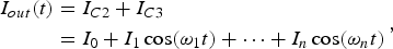 $$\eqalign{{I_{out}}(t) & = {I_{C2}} + {I_{C3}} \cr & = {I_0} + {I_1}\cos({\omega _1}t) + \cdots + {I_n}\cos({\omega _n}t)},$$
where I n is the nth-harmonic current component. The DC component I 0 in I out is:
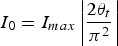 $${I_0} = {I_{max}}\left \vert {\displaystyle{{2{\theta _t}} \over {{\pi ^2}}}} \right \vert $$
and the second harmonic (I 2) in I out is:
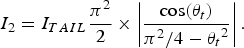
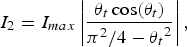 $${I_2} = {I_{max}}\left \vert {\displaystyle{{{\theta _t}\cos({\theta _t})} \over {{\pi ^2}/4 - {\theta _t}^2}}} \right \vert, $$
where θ t is the conduction angle. When t increases from 0 to t 0/2, V be2 decreases from V be_max to V be_on , as shown in Fig. 4:
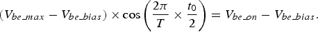 $$\left( {{V_{be\_max}} - {V_{be\_bias}}} \right) \times \cos \left( {\displaystyle{{2\pi} \over T} \times \displaystyle{{{t_0}} \over 2}} \right) = {V_{be\_on}} - {V_{be\_bias}}.$$
Hence, θ t can be expressed as a function of V be _bias , input power of LO signal (P LO ) and the input impedance of CECCTP frequency-doubling stage (R LO ):
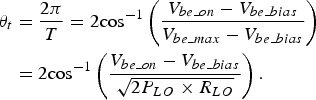 $$\eqalign{{\theta _t}& = \displaystyle{{2\pi} \over T} = 2{\cos ^{ - 1}}\left( {\displaystyle{{{V_{be\_on}} - {V_{be\_bias}}} \over {{V_{be\_max}} - {V_{be\_bias}}}}} \right) \cr&= 2{\cos ^{ - 1}}\left( {\displaystyle{{{V_{be\_on}} - {V_{be\_bias}}} \over {\sqrt {2{P_{LO}} \times {R_{LO}}}}}} \right).} $$
For simplicity, the transconductance performance of HBT is assumed to be constant when input power changes. Thus, current swing I max is proportional to the voltage swing V be_max – Vbe_on :
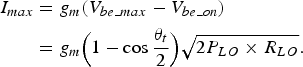 $$\eqalign{{I_{max}} & = {g_m}({V_{be\_max}} - {V_{be\_on}}) \cr & = {g_m}\Big(1 - \cos \displaystyle{{{\theta _t}} \over 2}\Big)\sqrt {2{P_{LO}} \times {R_{LO}}}.}$$
Since V be_bias is constant in Fig. 2(a), θ t drastically increases when P LO increases, as shown in equation (5). From equations (3) and (6), I 2 can be expressed as:
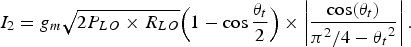 $${I_2} = {g_m}\sqrt {2{P_{LO}} \times {R_{LO}}} \Big(1 - \cos \displaystyle{{{\theta _t}} \over 2}\Big) \times \left \vert {\displaystyle{{\cos ({\theta _t})} \over {{\pi ^2}/4 - {\theta _t}^2}}} \right \vert. $$
Since I 0 is constant (I 0 = I TAIL ) and V be_bias is floated in Fig. 2(b), V be_bias decreases and θ t slightly decreases when P LO increases, as shown in equation (2). From equations (2) and (3), I 2 can be expressed as:
 $${I_2} = {I_{TAIL}}\displaystyle{{{\pi ^2}} \over 2} \times \left \vert {\displaystyle{{\cos ({\theta _t})} \over {{\pi ^2}/4 - {\theta _t}^2}}} \right \vert. $$
The I 2 in equation (7) has additional polynomials about θ t and P LO , compared with the I 2 in equation (8). Hence, a tail current source could make I 2 (2*f LO in I out ) insensitive to θ t , and meanwhile could make I 2 insensitive to P LO . It is expected that the SHM with the tail current source in Fig. 2(b) generates 2*f LO more smoothly than the SHM in Fig. 2(a).
Figure 5 shows the simulated dependence of 2*f LO (I 2 ) in I out on the LO input power in the conventional top-LO-configured SHM (gray solid line), the bottom-LO-configured SHM without I TAIL (black dashed line) and the improved bottom-LO-configured SHM with I TAIL (black solid line). Differential LO signal at 39.5 GHz is applied to the CECCTP frequency doubling stage. The improved SHM in Fig. 2(b) effectively enlarges and flattens the 2*f LO in I out with low LO input power range.

Fig. 5. Magnitude of the 2*f LO of I out .
III. CIRCUIT DESIGN
Figure 6 shows the schematic of the conventional top-LO-configured CECCTP SHM IC. HBTs Q1, Q2, and Q3 form the SHM core. The supply voltage for the conventional SHM core is 2.5 V. For on-wafer measurements, integrated Marchand balun is designed at the LO input port to transfer the differential balanced 50 Ω port to a single-ended unbalanced 50 Ω port. Since the center frequencies of LO and RF signals are 39.5 and 80 GHz, respectively, spiral inductors are utilized for the LO matching circuit and a microstrip line is used for the RF matching circuit.

Fig. 6. Schematic of the conventional top-LO-configured CECCTP SHM IC.
Figure 7 shows the schematic of the bottom-LO-configured SHM IC with a tail current source presented in this paper. HBTs Q1, Q2, Q3, Q4, and Q5 form the SHM core, where Q4 and Q5 serve as the tail current mirror. The supply voltage for the SHM core is 3.3 V. Both SHMs employ the same emitter follower as the IF buffer amplifier with a supply voltage of 1.8 V.

Fig. 7. Schematic of the improved bottom-LO-configured CECCTP SHM IC with tail current source.
Figures 8(a) and 8(b) illustrate the top and side views of the Marchand balun IC design, respectively. As shown in Fig. 8(a), a pair of coupled spiral transmission lines are employed for magnetic coupling and port transformation. As shown in Fig. 8(b), the microstrip line consists of a signal line using the top metal (M6) and a ground plane using the bottom metal (M1). The M1 and M6 are separated by a 10-µm thick dielectric material. The ground plane includes some square slots to meet the design rule. Since the line width, line space and balun size have large influence on the balun performance, the Marchand balun is simulated and analyzed by electro-magnetic solver, Momentum. Consequently, the line width and space are 6 and 3 µm, respectively, as depicted in Fig. 8(b). The balun size is 270×120 μm2 as shown in Fig. 8(a).

Fig. 8. (a) Top view and (b) side view of the Marchand balun IC.
Figure 9 shows the simulated dependence of the conversion power gain of both SHM ICs on the LO power. The frequencies of RF, LO, and IF signals are 80, 39.5, and 1 GHz, respectively. The RF power is fixed to −40 dBm, and LO power (P LO ) is swept from −20 to 10 dBm. The improved SHM in Fig. 7 has a conversion power gain of 6.9 dB (including the buffer gain) at P LO = −7 dBm. The core circuit of the improved SHM (without the buffer) consumes a DC current of 0.64 mA at a supply voltage of 3.3 V. The conventional SHM in Fig. 6 requires P LO = −1.5 dBm to have similar conversion power gain of 6.7 dB (including the buffer gain). The core of the conventional SHM (without the buffer) consumes a DC current of 0.27 mA at a supply voltage of 2.5 V. The dependence of the conversion gain on the LO power is similar to that of 2*f LO in I out shown in Fig. 5. In the top-LO-configured SHM, since the RF stage is the emitter degeneration for LO stage and the generation of 2*f LO is critically suppressed, the conversion gain is lower than that of the bottom-LO-configured SHM with P LO lower than −2 dBm. In the bottom-LO-configured SHM, since the LO stage becomes the emitter degeneration for RF stage and the transconductance of RF stage is limited, the conversion gain is lower than that of the top-LO-configured SHM with P LO higher than −2 dBm. As shown in Fig. 9, the conversion gain of the improved SHM is higher and less sensitive to the variation of P LO than that of the conventional one under P LO less than −2 dBm.

Fig. 9. Simulated dependence of the conversion gain on LO power.
Figure 10 shows the simulated double side band noise figure (DSB NF) of both SHM ICs with sweeping the LO power from −20 to 10 dBm. The frequencies of RF, LO, and IF signals are 80, 39.5 and 1 GHz, respectively. When P LO is lower than 0 dBm, the DSB NF of the improved SHM is much lower than that of the conventional SHM.

Fig. 10. Simulated dependence of the DSB NF on LO power.
The small signal noise analysis in GoldenGate is applied to simulate the noise level and the noise contribution of all the devices in the conventional and improved SHMs. Table 1 summarizes the simulated main noise contributors. The conventional and improved SHMs have the same conditions for simulation: f RF = 80 GHz, f LO = 39.5 GHz, f IF = 1 GHz, and P RF = −40 dBm. Since the optimal P LO is different between the two SHMs, P LO = −1.5 dBm is injected to the conventional SHM, while P LO = −7 dBm is injected to the improved SHM, respectively. In the conventional SHM, the RF stage (HBT Q1) is the biggest noise contributor with 86.8% noise contribution. In the improved SHM, the LO stage (HBTs Q2 and Q3) becomes the biggest noise contributor with 66% noise contribution, while the RF stage has only 5.1% noise contribution.
Table 1. Summary and comparison of the noise contribution in the conventional and improved SHM ICs.

The difference of the noise contribution is mainly caused by the difference of the operational principle. In the conventional SHM, the HBT Q1 (RF stage) enters the saturation region and increases the noise power. In addition, the noise of RF stage is amplified by the LO stage. Thus, the RF stage in the conventional SHM is the biggest noise contributor.
In the improved SHM, the LO stage generates the noise at the emitter of the HBT Q1 (RF stage). The noise from LO stage is amplified and converted to the noise at IF output by Q1. Thus, the LO stage in the improved SHM is the biggest noise contributor.
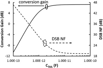
Since the noise coming from the tail current source (Q4 and Q5) is shunted by the C TAIL , the tail current source has only 6.4% noise contribution. Figure 11 shows the dependence of conversion gain and DSB NF on the C TAIL of the improved SHM. The conditions for the simulation are the same as those for the noise contribution simulation. As shown in Fig. 11, a large C TAIL for AC ground is necessary to increase the conversion gain and decrease the DSB NF. Consequently, C TAIL is chosen to 10 pF in the improved SHM circuit. The C TAIL for AC ground decreases the common-mode rejection of the tail current source and might be a source of instability for a common-mode signal. It is confirmed that the SHM IC is stable from the transient simulation with sweeping LO power.

Fig. 11. Simulated conversion gain and DSB NF of the improved SHM versus C TAIL .
Figure 12 shows the simulated port-to-port isolation, including the 2LO–RF, LO–RF at the RF port, and the RF–IF, 2LO–IF, LO–IF at the IF port of the (a) conventional and (b) improved SHM ICs. The isolations are simulated as a function of LO frequency (f LO ). The f LO is swept from 37.5 to 41.5 GHz and the f RF is correspondingly changed from 76 to 84 GHz to keep the f IF fixed to 1 GHz. Both two SHMs are applied with the RF power of −40 dBm. The conventional and improved SHMs are applied with the LO power of −1.5 and −7 dBm, respectively. Both SHMs have excellent LO–RF isolation as a result of the CECCTP structure of the LO stage and the balance of the balun.

Fig. 12. Simulated isolation of the (a) conventional SHM and (b) improved SHM versus LO and RF frequency (f IF = 1 GHz).
Figure 13 shows the simulated input–output response of the conventional and improved SHM ICs. The frequency conditions for the simulation are: f RF = 80 GHz, f LO = 39.5 GHz, and f IF = 1 GHz. The LO power of −1.5 and −7 dBm are injected to the conventional and improved SHMs, respectively. The IP1 dB and OP1 dB of the conventional SHM are −27.0 and −21.5 dBm. The IP1 dB and OP1 dB of the improved SHM are −23.0 and −17.0 dBm. In the conventional SHM, since the RF stage enters the saturation region as shown in Fig. 3, the voltage swing of the IF signal is suppressed. Thus, the IP1 dB of conventional SHM is lower than that of the improved one.

Fig. 13. Simulated IF output power versus RF input power.
Figure 14 shows the simulated conversion gain of the conventional and improved SHMs as a function of the RF frequency. The f LO is swept from 37.5 to 41.5 GHz and the f RF is correspondingly changed from 76 to 84 GHz to keep the f IF fixed to 1 GHz. The conventional and improved SHMs are applied with an LO power of −1.5 and −7 dBm, respectively.

Fig. 14. Simulated conversion gain versus RF frequency.
IV. MEASUREMENT RESULTS
A) Measured results of the Marchand balun
To confirm the performance of the Marchand balun, a balun IC is individually fabricated in 130-nm SiGe BiCMOS technology. Figure 15(a) shows the die photograph of the balun IC and the core size is only 270×120 µm2. Figure 15(b) shows the measured insertion loss performance. From 26 to 66 GHz, the balun IC exhibits measured insertion loss of <3 dB. Figure 15(c) illustrates the measured imbalance performance. From 20 to 66 GHz, the amplitude imbalance is <0.9 dB and the phase imbalance is <2.5°.

Fig. 15. (a) Die photograph of the Marchand balun IC, (b) measured insertion loss, (c) measured amplitude and phase imbalance.
B) Measured results of the SHM ICs
Figure 16 shows the die photograph of the bottom-LO-configured CECCTP SHM IC with a tail current source presented in this paper, which has a core size of 550 by 460 µm. In addition, the conventional top-LO-configured CECCTP SHM IC is fabricated for comparison.

Fig. 16. Die photograph of the improved bottom-LO-configured SHM IC with tail current source.
Figure 17 shows the measured dependence of the conversion power gain of the improved and conventional SHM ICs on the LO power. The measurement was carried-out on-wafer with single-ended 50-Ω system. At an RF frequency of 80 GHz and an LO frequency of 39.5 GHz (IF output frequency is 1 GHz), the improved SHM IC achieves a conversion power gain of 3.9 dB and a DC power consumption of 2.2 mW at an LO power of only −7 dBm. Considering the insertion loss of the balun as shown in Fig. 15(b), the actual input power is around −9 dBm. The conventional top-LO-configured one has a conversion power gain of 1.9 dB with a power consumption of 1.1 mW at an LO power of −1.5 dBm.

Fig. 17. Measured dependence of the conversion gain on the LO power (conditions: f RF = 80 GHz, f LO = 39.5 GHz, f IF = 1 GHz).
Figure 18 shows the simulated and measured input return loss at: (a) LO port and (b) RF port of the improved SHM IC with −7 dBm LO input power injected. The return loss of the LO port is better than 10 dB from 36.1 to 40.6 GHz. The return loss of the RF port is better than 10 dB from 78 to 82.7 GHz. The measured return losses well agree with the simulation.

Fig. 18. Measured and simulated input return loss of the (a) LO port and (b) RF port of the improved SHM IC.
Figure 19 depicts the simulated and measured IF frequency responses of the conversion gain of the improved SHM IC. RF frequency is fixed to 80 GHz and RF power is fixed to −37 dBm. LO input power is fixed to −7 dBm and LO frequency is swept from 39.95 to 39.25 GHz. Thus, IF frequency changes from 100 MHz to 1.5 GHz. When IF frequency is below 200 MHz, the conversion gain decreases with IF frequency decreasing because the capacitors are not large enough for DC block and AC ground. When the IF frequency is above 500 MHz, the conversion gain decreases with IF frequency increasing as a result of the frequency response of the buffer amplifier.

Fig. 19. Measured and simulated conversion gain versus IF frequency of the improved SHM IC (conditions: f RF = 80 GHz, f LO = (f RF – f IF )/2, P LO = −7 dBm).
Figure 20 shows the simulated and measured input–output responses of the improved SHM IC with an LO power of −7 dBm at 39.5 GHz. The frequencies of RF and IF signals are 80 and 1 GHz, respectively. The measured IP1 dB and OP1 dB are −27 and −25 dBm, respectively.

Fig. 20. Measured and simulated IF power versus RF power of the improved SHM IC (conditions: f RF = 80 GHz, f LO = 39.5 GHz, f IF = 1 GHz, and P LO = −7 dBm).
Table 2 summarizes the measured performance of the fabricated CECCTP SHM ICs with previously published W-band SHM ICs. W-band SHM ICs utilizing the passive sub-harmonically pumped (SHP) diode topology require high LO power and suffer from the conversion loss. Compared with the active SHMs in [Reference Hung, Hancock and Rebeiz5, Reference Tsai, Yang, Huang and Wang15, Reference Ning26], the LO-bottom-configured SHM IC presented in this paper has exhibited higher conversion gain with lower LO power and ultra-low power consumption.
Table 2. Summary and comparison of the W-band SHM ICs.

* Includes 11 dB gain of the IF buffer amplifier.
† Includes 2 dB insertion loss of the balun.
‡ SHP, sub-harmonically pumped.
V. CONCLUSION
A bottom-LO-configured CECCTP SHM IC with a tail current source for W-band applications has been designed, fabricated, and tested using 130-nm SiGe BiCMOS technology. The SHM IC exhibits a conversion gain of 3.9 dB at 80 GHz with an LO power of only −7 dBm at 39.5 GHz. The DC power consumption of the SHM IC is only 2.2 mW. It is confirmed that the bottom-LO-configuration decreases the requirement of LO power and the tail current source makes the conversion gain insensitive to the variation of LO power. Therefore, the improved SHM topology significantly facilitates the design of oscillator and is suitable for W-band transceiver IC.
ACKNOWLEDGEMENT
The authors would like to thank Keysight Technologies Japan Ltd. for EDA support.
 Xin Yang participated a 3 + 2 joint training project and received the B.S. degree from Southeast University, Nanjing, China, and M.S. degree from Waseda University, Japan, in 2013, respectively. Currently, he is working toward Ph.D. degree at the Graduate School of Information, Production and Systems, Waseda University, Kitakyushu, Japan. His research interests include the microwave and millimeter-wave integrated circuits.
He received the Best Student Paper Award of IMWS2012, and Young Engineer Prize of the 10th EuMIC (2015).
 Xiao Xu was born in Changzhou, China, in 1992. He received the B.E. degree in Electronics Engineering from Southeast University of China in 2015. Since September 2013, he has been a Master student in the Graduate School of Information Production and Systems of Waseda University in Japan.
 Takayuki Shibata received the B.E. degree in physics from the Tokyo Metropolitan University in 1992 and joined DENSO CORPORATION. His main research interests are microwave power transmission and high-frequency integrated circuit.
 Toshihiko Yoshimasu received the B.S. and Ph.D. degrees in Electrical Engineering from Kobe University, Kobe, in 1981 and 1999, respectively. In 1981, he joined Central Research Laboratories of Sharp Corporation, Tenri, Japan. From 1981 to 1984, he was engaged in research and development on high-power Si MOSFETs. From 1985 to 1999, he was engaged in research and development on GaAs-based microwave devices and associated monolithic circuits, including low-noise amplifiers, power amplifiers, switches, filters, oscillators, and frequency converters. From 2000 to 2003, he was involved in the research and development of Si CMOS RF ICs for wireless communications. Since April 2003, he has been a Professor of the Graduate School of Information, Production and Systems, Waseda University, Kitakyushu-shi, Japan. His major interests include microwave and millimeter-wave ICs with Si CMOS, SiGe BiCMOS, GaAs-based HBT, and pHEMT technologies. Dr. Yoshimasu is a senior member of the Institute of Electronics, Information and Communication Engineers (IEICE), and a member of the Institute of Electrical and Electronics Engineers (IEEE). Dr. Yoshimasu was also an associate editor of IEICE Electronics Express (ELEX) from 2011 to 2014.