


I. INTRODUCTION
After the allocation of the frequency band from 3.1 to 10.6 GHz for the commercial use of ultra-wideband (UWB) systems by the Federal Communication Commission, UWB systems have received phenomenal gravitation in wireless communication. UWB radio technology has found application in medical imaging systems, pulse communication, ground penetration radar, and so on. Designing an antenna to operate in the UWB band is quite a challenge because it has to satisfy the requirements such as ultra wide impedance bandwidth, omnidirectional radiation pattern, constant gain, high radiation efficiency, low profile, easy manufacturing, and etc [Reference Fakharian and Rezaei1].
In UWB communication systems, one of the key issues is the design of a compact antenna while providing wideband characteristic over the whole operating band. Consequently, a number of UWB antennas with different geometries have been experimentally characterized [Reference Wang, Yin, Liu and Wang2–Reference Fakharian, Rezaei and Azadi4]. Among them, planar monopole antennas are considered as good candidates for UWB applications due to their attractive merits, such as large impedance bandwidth, easy fabrication, and omnidirectional radiation pattern [Reference Foudazi, Hassani and Nezhad5]. Especially in the case of microstrip UWB planar monopole antenna, different methods have been utilized in the articles to design a UWB antenna with various band-notched properties [Reference Abed, Kimouche and Lembrikov6–Reference Sarkar, Rakshit, Adhikari, Pal and Ghatak9]. Despite the advantages of UWB systems, there are many narrowband communication systems which severely interfere with the UWB communication system, such as worldwide interoperability for microwave access (WiMAX) (3.3–3.6 GHz), C-band (3.7–4.2 GHz), wireless local area network (WLAN) (5.15–5.35 GHz and 5.725–5.825 GHz), high performance radio LAN (HIPERLAN)/2 (5.47–5.725 GHz), and dedicated short-range communications (DSRC) (5.85–5.925 GHz). Therefore, UWB antennas with band-notched characteristics to filter this potential interference are desirable. The band-notched characteristics could be achieved by many techniques such as embedding of open-end slit to the antenna structure and addition of a tuning stub within the antenna structure or the ground plane [Reference Sarkar, Rakshit, Adhikari, Pal and Ghatak9], inserting different types of slots on the radiating patch or associated ground plane [Reference Li, Hei, Feng and Shi10–Reference Azim and Islam12], addition of parasitic elements near the printed antennas [Reference Jiang and Che13], using different shapes of conductor-backed plane structures [Reference Ojaroudi, Ojaroudi and Mirhashemi14], locating filtering structures in the vicinity of the feed line [Reference Sung15], and so on. Among these methods, the primary methods are inserting λ/2 or λ/4 slots or stubs on the patch, fed-line or the ground plane. There are kinds of shapes for the slots and the stubs, such as U-shaped [Reference Lee, Lim and Yu7], H-shaped [Reference Sung8], C-shaped [Reference Chu and Yang16], L-shaped [Reference Farrokh-Heshmat, Nourinia and Ghobadi17], π-shaped [Reference Valizade, Ghobadi, Nourinia and Ojaroudi18], and Ω-shaped [Reference Li, Shi and Hei19]. Employing one structure sometimes can obtain multiple notched bands [Reference Sung8], or multiple notched band structure only introduce one resonance [Reference Zheng, Chu and Tu20], which make it hard to analysis and adjust the notched band. On the other hand, in some designs, the bandwidth of the notched bands is somewhat too wide so that useful signal is shielded at the same time [Reference Lee, Yang and Cho21, Reference Zhu, Gao, Ho, Abd-Alhameed, See, Li and Xu22].
In this paper two methods for designing a novel and compact microstrip-fed monopole antenna with dual band-notched characteristic for UWB applications has been designed and manufactured. In the proposed structure a bat-shaped radiating patch is used to achieve a multi-resonance performance. By embedding the resonance elements, the proposed design can reject the frequency bands with central frequencies at 3.5 and 5.6 GHz without using an additional band-stop filter. By inserting the half-wavelength spiral-slots on the radiation patch, good band-notched performance with a high level of signal rejection can be achieved. While the other notched band is acquired by inserting folded stepped impedance resonator (SIR) as defected ground structure (DGS) on the ground plane of the antenna. These structures can resonant independently with tiny interference among them. An equivalent circuit model of the proposed dual band-notched UWB antenna is extracted to explain the dual band-notched characteristics. Good reflection coefficient, radiation pattern, and group delay characteristics are obtained in the frequency band of interest. The simulated results are identical with the measured ones reasonably.
II. ANTENNA DESIGN AND CONFIGURATION
Figure 1 shows the geometry of the dual band-notched UWB bat-shaped monopole antenna fed by a 50-Ω microstrip line. The antenna is printed on a low-cost FR4 substrate of thickness 1.6 mm, permittivity 4.4, and loss tangent 0.02. The bat-shaped radiating element and feeding line are printed on the top side of the dielectric substrate and a rectangular ground plane on the bottom side. In order to create single and dual band-filtering, spiral-slots and a SIR-DGS are inserted at radiating patch and ground plane, respectively. Figure 2 shows the approximate equivalent circuit model of the proposed dual band-notched UWB antenna [Reference Abed, Kimouche and Lembrikov6, Reference Yu, Wang and Matin23, Reference Wei, Xu, Shi and Liu24].

Fig. 1. Geometry of the proposed dual band-notch UWB antenna. (a) Top and (b) bottom view of the antenna, (c) parameters of spiral-slots and (d) SIR-DGS.

Fig. 2. Approximate equivalent circuit model for the proposed dual band-notch UWB antenna.
The radiation patch has a bat-shaped structure, and the dimensions are improved using commercial software. The final design parameters of the UWB antenna are as follows: L = 27 mm, W = 19 mm, L g = 4.5 mm, W f = 3 mm, h 1 = 0.7 mm, h 2 = 1.9 mm, h 3 = 4 mm, h 4 = 15 mm, h 5 = 9 mm, h 6 = 4.9 mm, h 7 = 18.4 mm, d 1 = 6 mm, d 2 = 4.5 mm, d 3 = 5 mm, d 4 = 10.8 mm, d 5 = 6.7 mm, r 1 = 0.7 mm, r 2 = 1.3 mm, r 3 = 2 mm, r 4 = 2.7 mm.
By examining the current distribution of planar monopole antenna with regular shapes, i.e. rectangular, circular, etc., the proposed cuttings in the bat-shaped monopole antenna are used to increase the antenna perimeter. It affects the lower resonant frequency and then increasing the maximum achieved impedance bandwidth [Reference Ahmed and Sebak25, Reference Azenui and Yang26]. It is well known that the current distribution is mainly concentrated in the edges rather than in the center of the printed monopole antenna. Thus, by increasing the antenna perimeter p, the surface current will take longer path and this will be equivalent to a longer length monopole and in turn will decrease the lowest resonance frequency f L [Reference Ahmed and Sebak27]:
 $$\varepsilon _{eff} \approx \displaystyle{{(\varepsilon _r + 1)} \over 2}, $$
 $$f_L (\rm GHz) = \displaystyle{{300} \over {p\sqrt {\varepsilon _{eff}}}}, $$
where ε eff is the approximated effective dielectric constant and the perimeter unit is in millimeters.
For UWB antenna, the radiating element can be modeled by several adjacent resonances and each one can be represented by an RLC parallel circuit [Reference Chu and Yang16]. Approximately, the radiating element of the proposed UWB antenna can be seen as several parallel RLC cells in series, as shown in Fig. 2. Figure 3 shows the characteristics of the simulated reflection coefficient (|S 11|) of the UWB antenna by using Ansoft HFSS and CST Microwave Studio. A relative good agreement in between simulations can be observed. It is found that the |S 11| of the antenna is well matched as the bandwidth covers the entire UWB frequency range 3.1–10.6 GHz and goes beyond the required 10.6 GHz with |S 11| ≤ –10 dB.

Fig. 3. Simulated |S 11| of the proposed UWB antenna.
To design a novel UWB monopole antenna, a bat-shaped radiating patch is used as initial structure in the proposed antenna, as displayed in Fig. 1(a). Three bat-shaped patch with different sizes are specified in Table 1 as cases 1–3. Figure 4 shows the effects of it with different values on the impedance matching. It is found that by setting the bat-shaped patch to suitable dimensions, the wider impedance bandwidth with multi-resonance characteristics can be produced, especially at the lower and higher bands.

Fig. 4. The simulated |S 11| characteristics for the three cases of UWB antenna with different values of bat-shaped radiating patch.
Table 1. Three cases of UWB antenna with different values of bat-shaped radiating patch.

A) Spiral-slots as notch band structure
In order to eliminate interferences from WLAN, HIPERLAN/2, and DSRC systems with the UWB, spiral-slots are etched on the radiating patch as a band rejection structure to cover the interval 5.15–5.925 GHz. As shown in Fig. 1(c), the spiral-slots are obtained by etching two separated spiral patterns which have same size and inverse split direction in the radiating patch. They are connected together by a rectangular-slot. The relationship between the notched frequency and the total length of spiral-slots can be summarized as following equations,
 $$\eqalign{&L_{cir} \,= \left[ {\left( {\sum\limits_{i = 1}^t i} \right) \times 2\pi W_{sp}} \right] - t \times W_{sp}, \cr & \quad L = 2L_{cir} + L_{sp} - W_{sp}\, f_{notch} = \displaystyle{c \over {2L \times \sqrt {\varepsilon _{eff}}}},} $$
where c is the speed of light in free space, t is the spiral turn, L cir is the length of the spiral-slot, and L presents the total length of the slot. We can take (2) into account in obtaining the total length of the spiral-slots at the very beginning of the design and then adjust the geometry for the final design. At the notch frequency, current concentrates around the spiral-slots. In Fig. 5, since the antenna operates in a transmission-line-like mode [Reference Chu and Yang16], the impedance is very high (open circuit) at the middle of rectangular-slot and the impedance is nearly zero (short circuit) nearby the center of spiral-slots. The zero impedance at the feeding point leads to the desired impedance mismatching at the notch frequency. Therefore, the spiral-slots can be modeled as a half-wavelength shorted parallel stub to act as the shunt series LC resonant for the band pass filter, as shown in Fig. 2. L s and C s indicate the inductor and capacitor values of the slot resonator. When the current propagates along the edge of the slot, an inductance should be introduced to the model. The narrow slot is equivalent to a capacitor. Increasing the length of the slot or decreasing the slot width is similar to increasing the capacitor value in the parallel LC circuit. On the other hand, increasing the length of slot will also lead to the increase of the inductor value [Reference Yu, Wang and Matin23]. It is found that by adjusting the total length of the spiral-slots to be approximately half-wavelength of the desired notched frequency, a destructive interference can take place, causing the antenna nonresponsive at that frequency. The final dimensions of the spiral-slots are as follows: L sp = 4.6 mm, W sp = 0.1 mm, g sp = 0.06 mm, D sp = 1.4 mm, and t = 3.5 turn.

Fig. 5. Surface current around the spiral-slot of the proposed antenna at the notch frequency.
It is easy to tune the notch center frequency with the change in total length of the slot. The effects of two different parameters t and L sp of the slot on the band rejection performance of the presented design are also studied and shown in Fig. 6, where t is the spiral turn and L sp is the length of the rectangular-slot. As observed in Fig. 6(a) that, the notched frequency is shifted from 5.6 to 7 GHz when t decreases from 3 to 2. Moreover, the increase in the bandwidth of the notched band can be observed with this change. Therefore, a wide notched band is obtained over the UWB frequency band when t is 2. It is also found that the performance of the reflection coefficient near 12 GHz becomes poor when t is 3. Taking the consideration of the performance and limited space for inserting the band-rejected elements, 3 is chosen for t in the design. In Fig. 6(b), when L sp changes from 2.7 to 4.7 mm, the center frequency of the notched band moved from 6.3 to 5.6 GHz. These indicate that the center frequency of the notched band decreases as the length of the rectangular-slot increases. Interestingly, it is also found that the bandwidth of the reflection coefficient becomes wider when L sp is shorter. It should be highlighted that, the value more than 4.7 mm is not considered to avoid the fabrication error. Since the notched band can cover 5–6 GHz when L sp is equal to 4.7 mm, the length of the rectangular-slot is selected to be 4.7 mm.

Fig. 6. Variation of reflection coefficient in terms of (a) t and (b) Lsp.
B) Folded SIR-DGS as notch band structure
Besides WLAN, HIPERLAN/2, and DSRC systems, WiMAX and C-band may cause interferences to the UWB system too. By etching a folded SIR-DGS as band-notched structure on the ground plane, a band-notched function can be realized to cover the interval 3.3–4.2 GHz. As shown in Fig. 1(d), the folded SIR-DGS consists of low–high–low impedance slots, and the slots are etched on the ground plane. From the equivalent circuit model of Fig. 2, by inserting folded SIR defective pattern in the ground plane a parallel LC resonant circuit is added to the equivalent circuit. From the resonance condition Z in = 0, the resonant frequency of a half-wavelength resonator can be deduced as follows,
 $$\eqalign{L &= 4L_s + W_s + 2S_4 + 2S_3 - 2S_1 - 2g_1, \cr f_{notch} & = \displaystyle{c \over {2L \times \sqrt {\varepsilon _{eff}}}}} $$
where L is the total length of the folded SIR-DGS. The improved parameters of the folded SIR-DGS are as follows: W s = 4 mm, L s = 4 mm, g 1 = 0.16 mm, g 2 = 0.36 mm, S 1 = 0.27 mm, S 2 = 0.52 mm, S 3 = 0.44 mm, and S 4 = 1.8 mm.
In order to better analyze the effect of these parameters, a quasi-static equivalent circuit model of the folded SIR-DGS is given in Fig. 7. The quasi-static equivalent circuit model is directly derived from the physical dimensions of DGS [Reference Karmakar, Roy and Balbin28]. Figure 7(a) shows the equivalent filament model of the folded SIR-DGS. The current distribution of this compact model is shown in Fig. 7(b). As can be seen in this figure of the folded SIR-DGS perturbed microstrip transmission line, the return path of the current is fully disturbed and this current is confined to the periphery of the perturbation and returns below the microstrip line once the perturbation is over. Based on the observation of the maximum concentration of the return current, the width of the side filament arms, which contribute to the inductance of the folded SIR-DGS, is selected.

Fig. 7. (a) Equivalent filament model and (b) surface current of truncated structure of folded SIR-DGS on ground plane. (c) Quasi-static equivalent circuit model.
Figure 7(c) shows the equivalent-circuit model of the folded SIR-DGS. Taking into consideration the aforementioned closed-form expressions and circuit parameters, we model the equivalent circuit of the truncated figure and then carry on the following conversions using the two-port circuit parameters. The width of the ports considered here corresponds to 50-Ω characteristic impedance. The gap is represented by the equivalent capacitances and is connected vertically to the arms of the two crosses. The power is impinged at one arm of the cross and power is extracted from the opposite arm of another cross. Now the equivalent-circuit model of the current filament can be extracted with the equivalent inductances and capacitances of the microstrip discontinuities. The inductances and capacitances are derived from the physical dimensions using quasi-static expressions for microstrip crosses, bent lines, and gaps capacitances are fully characterized by 17 equations in the literature [Reference Karmakar, Roy and Balbin28]. All these expressions take care of the dimensions of the DGS and the dielectric properties of the substrate. Therefore, from the equivalent-circuit model, a direct correlation between the design parameters and the design specification is calculated. The gaps are represented by two parallel capacitances to ground (C P ) and a series capacitance (C GAP ). The values of these capacitances are extracted from even- and odd-mode capacitances. Interestingly, it should be noted that all equivalent capacitances are extracted from the physical dimensions of the gap discontinuity and the dielectric constant [Reference Garg and Bahl29]. If two conductors meet at an angle, mutual inductance comes to play at the bend, which we represented as L bend in the circuit diagram (Fig. 7(c)). Two sets of two symmetrical arms of the microstrip cross are represented by equivalent L 1, L 2, C +, and the cross arms are inductively coupled by L 3. The equivalent capacitances and inductances are calculated in the literature [Reference Garg and Bahl29].
To compare the frequency response characteristics of the folded SIR-DGS, a two-port filter structure consisting of a combination of a resonator and a 50-microstrip line is simulated. The structure is printed on the substrate with a permittivity of 4.4 and a thickness of 1.6 mm. The transfer characteristics of the folded SIR-DGS with various dimensions are shown in Fig. 8. It can be seen that the notched band decreases as W s and S 4 increase. But the notched band increases as g 1 increases. Also by changing the g 1 of the folded SIR-DGS, we can change the width of the notched band. Therefore the notched band can be obtained at the desired frequency by appropriately adjusting the resonator dimensions. Moreover, by the electrical model in Fig. 7, a physical insight into the behavior of the antenna is given for the parametric analysis in Fig. 8. The variation of the resonant frequencies of the folded SIR-DGS with the arm length W s and S 4 are due to the fact that when these parameters increase the inductance from the folded SIR-DGS increases, hence, the resonant frequency of the parallel circuit decreases. The variation of the resonant frequency with the gap distance g 1 is due to the fact that when the gap distance increases, the gap capacitance diminishes. As a result, the resonant frequency increases with the increase of the gap distance.

Fig. 8. Transfer characteristics of the SIR-DGS for various dimensions, (a) W s , (b) S 4, and (c) g 1.
III. RESULTS AND DISCUSSION
The proposed dual band-notch UWB antenna with final modified design parameters, as shown in Fig. 9, was built and tested. Figure 10 shows the simulated and measured |S 11| characteristics of the antenna. Simulation is carried out using Ansoft HFSS, a commercial three-dimensional (3D) electromagnetic simulator based on finite element method. The fabricated antenna has the frequency band of 2.83 to 11.56 GHz with two rejection bands around 3.3–4.2 and 4.9–6 GHz. The simulated gain and the measured one decrease over these two band-notched frequencies, as shown in Fig. 11. However, as shown in Figs 10 and 11, there exists a discrepancy between the measured data and the simulated results. This discrepancy is mostly due to a number of parameters such as fabrication inaccuracies (e.g. over-etching), uncertainties in the substrate thickness and effective permittivity, the wide range of simulation frequencies, and so on. However since substrate materials may vary among manufacturers, the design methodology, and proof of concept are the main foci of this work. In order to confirm the accurate reflection coefficient characteristics for the designed antenna, it is recommended that the manufacturing and measurement processes need to be performed carefully. Moreover, SubMiniature version A (SMA) soldering accuracy and FR4 substrate quality need to be taken into consideration.

Fig. 9. Photograph of the realized printed monopole antenna, (a) top view, and (b) bottom view.

Fig. 10. Measured and simulated |S 11| characteristics of the antenna.
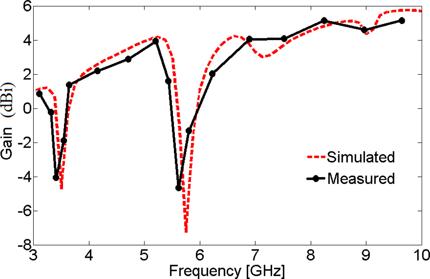
Fig. 11. Measured and simulated gains of the antenna.
To give a better insight about the dual band-notch behavior of the proposed antenna, a simulated input impedance characteristic at the band-notch performance is shown on a Smith chart in Fig. 12.

Fig. 12. Input impedance performance of the proposed antenna.
Measurement set-up of the antenna for the radiation pattern characteristics is shown in Fig. 13. Figure 14 depicts the measured far-field radiation patterns for the proposed dual-band notched UWB antenna in the E-(xy-) and H-(xz-) planes at 3, 6.5 and 10 GHz. It is observed that nearly omnidirectional radiation patterns are obtained on H-plane over the whole UWB frequency range. The radiation patterns on the E-plane are monopole-like with bidirectional patterns in a very wide frequency band. It is observed that the radiation pattern is slightly tilted off-broadside. The beam tilt is due to the asymmetrical geometry of the patch antenna, compared with a simply patch which has a symmetrical geometry and shows a broadside beam. As the frequency goes up, tiny distortions occur. This is because the electrical length of the antenna increases at higher frequency.

Fig. 13. Measurement set-up of the antenna for radiation patterns.

Fig. 14. Measured radiation patterns of the proposed antenna in the E- and H-planes at (a) 3 GHz, (b) 6.5 GHz, and (c) 10 GHz.
To analyze the signal dispersion, the group delay is simulated between two identical antennas in the face-to-face orientations, with a distance of 300 mm between them, which obtains the far-field condition of the antenna. As shown in Fig. 15, the group delay is about 1 ns across the frequency band except in the notched bands, due to the band-notched function. For the rest of the frequency band, the group delay characteristic is relatively flat, indicating that the antennas have good linear transmission performances.

Fig. 15. Simulated group delay of the proposed antenna.
As the UWB communication has been based on impulse radio, it is necessary to consider the impulse distortion of the time-domain response of the proposed antenna. In telecommunication systems, the correlation between the input and output signals is evaluated using the fidelity factor F (1),
 $$F = {\max_{\tau}} \left\vert {\displaystyle{{\int_{ - \infty} ^{ + \infty} {s(t)r(t - \tau )}} \over {\sqrt {\int_{ - \infty} ^{ + \infty} {s(t)^2 dt.\int_{ - \infty} ^{ + \infty} {r(t)^2 dt}}}}}} \right\vert, $$
where s(t) and r(t) are the input and output signals, respectively. To calculate the fidelity factor of the proposed dual-band notched UWB antenna, it is assumed that the two proposed antennas in Fig. 1 play the role of the transmitting antenna and receiving antenna. The two antennas are aligned pointing face-to-face and side-by-side orientations with a distance of 300 mm. The input signal s(t) form of the Gaussian pulse can be excited to transmitting antenna, then receiving pulse signal r(t) can be obtained to receiving antenna. This pulse simulation is performed by a CST Design Studio simulator. By substituting the two normalized pulse signal in equation (5), we can calculate the fidelity factor F which is the maximum correlation coefficient between two pulse signals. The antenna having F = 1 indicates a perfect match between s(t) and r(t), without distortion in the transmission system of the pulse signal. The fidelity factor F of the proposed dual-band notched UWB antenna for the face-to-face and side-by-side configurations were obtained equal to 0.92 and 0.86, respectively. Values of the fidelity factor show that the proposed UWB antenna exhibits a good time domain performance in the view of operating UWB communication systems.
IV. CONCLUSION
A dual band-notched UWB antenna has been proposed and designed by introducing the folded SIR-DGS and the spiral-slots as band-rejected elements. In this design, the proposed antenna can operate from 2.83 to 11.56 with two rejection bands around 3.3–4.2 and 4.9–6 GHz. Parametric studies, relevant equations and the equivalent circuit model of the antenna provide guidelines on how to understand the mechanism of band-notched characteristics. Good agreement between the simulated and measured results including stable radiation patterns, gain, and low |S 11| (except for the notched bands) for all radiating frequencies is obtained. It demonstrates that the proposed antenna is suitable for application in UWB system.
 Seyed Saeed Mirmosaei was born in Ramsar, Iran, in 1986. He received his B.S. degree in Electrical Engineering from Guilan University, Rasht, Iran, in 2008. Currently, he is working towards the M.Sc. degree in Communication Engineering from Shahid Beheshti University, Tehran, Iran. His research interests include ultra-wideband monopole antennas.
 Seyed Ebrahim Afjei received his B.S. and M.S. degrees in Electrical Engineering from the University of Texas in 1984, 1986, respectively, and the Ph.D. degree from New Mexico State University, in 1991. He is currently a Professor and Dean of the Department of Electrical Engineering, Shahid Beheshti University G.C., Tehran, IRAN. His research interests are in the areas of switched reluctance motor drives, numerical analysis, and power electronics.
 Esfandiar Mehrshahi was born in Tehran, Iran, in 1963. He received his B.Sc. degree from the Iran University of Science and Technology, Tehran, Iran, in 1987, and the M.Sc. and Ph.D. degrees from the Sharif University of Technology, Tehran, Iran, in 1991 and 1998, respectively, all in Electrical Engineering. Since 1990, he has been involved in several research and engineering projects at the Iran Telecommunications Research Center (ITRC). He is currently an Assistant Professor at Shahid Beheshti University, Tehran, Iran. His main areas of interest are the nonlinear simulation of microwave circuits, computational electromagnetics, and low phase noise oscillators.
 Mohammad M. Fakharian was born in Tehran, Iran, in 1987. He received his B.S. and M.S. degrees in Electrical Engineering from Semnan University, Semnan, Iran, in 2009 and 2012, respectively. Currently, he is working towards the Ph.D. degree in Communication Engineering from Semnan University. His research interests include low-profile printed and patch antennas for wireless communication, fractal, miniature and multiband antennas, meta-materials and EBG structures interaction with antennas and RF passive components, reconfigurable antennas, and electromagnetic theory: numerical methods and optimization techniques.


