


I. INTRODUCTION
Switched-line phase shifters (SLPS) are suitable for constant time delay to develop true-time-delay (TTD) networks, well known for their accurate linear trend in frequency phase shifts along enough wide bands, essential for the precise beam-forming required for phased array applications. Since agile beams of electronically scanned arrays provide significant system advantages, phased-array technology is receiving considerable attention by the military and industry for airborne, space, surface, and ground-based applications [Reference Parker1–Reference Van Bezouwen, Feldle and Holpp4].
Phased arrays are immobile ensemble of antennas in which, by varying the progressive phase excitation of each component, the beam can be oriented in any direction. This approach is widely used in both military and civilian applications. However, wide bandwidth is not available employing traditional electrical feeding networks due to their intrinsic narrow band nature. Conventional phase shift for a specific steering angle is decoupled from scanning frequency, resulting in beam squinting when the frequency changes. This is the problem that affects constant phase (CP) shifters.
Wide aperture arrays for transmitting and receiving wide band signals suffer beam broadening when steered away from the array normal using phase delays between the array elements. This beam dispersion is eliminated if time delays instead of phase shifts are used between antenna array elements [Reference Gesell and Feinleib5–Reference Ta-Shun and Hashemi8].
TTD steering techniques are necessary to make the far-field pattern independent of the microwave frequency. If time shift is set according to a particular steering direction, then the microwave phase shift can follow the frequency scan to avoid beam squinting [Reference Helmy and Entesari6, Reference Chen, Wu, Zhao, Kim and Chen9]. In terms of phase, a TTDL is a phase shifter with linear phase variation with frequency. This result from the fact for a constant phase velocity, the wave number is proportional to the frequency [Reference Legay10].
The most popular TTD configurations are: SL type, reflection type, and distributed type [Reference Garver11].
The SL type [Reference Gao, Zheng, Bai and Qin12, Reference Yang, Lee and Yang13] is based on different length transmission lines which are switched to produce different delays. It has an excellent performance over a large bandwidth but the size of this device is its major drawback. The bandwidth is not limited by the dispersion in the line but rather by the quality of the switching devices.
For applications where space saving is a major issue, a sensible choice is the reflection type [Reference Li, Kuo, Wu, Cheng, Huang and Tsai14, Reference Di Paolo15], which reduces the length of the lines by two by taking advantage of the reflected wave. From this point of view, the reflection type is rather an evolution of the switched type than a completely new topology. The limitation on this device is also fixed by the switches but even more significantly the 3-dB coupler needed at the input which will limit the bandwidth performance of the device. The problem is usually addressed using a Lange coupler, which guarantees an acceptable bandwidth. However, this type of design is still not suitable if wide bandwidth is a strong specification.
The distributed type is most performing in the highest frequencies (above 20 GHz), when compared with the other types [Reference Du, Bao, Wu, Cheng and Mu16, Reference Bovadilla, Rehder, Serrano and Ferrari17]. This kind of TTD takes advantage of the fact that the wave velocity depends on the line-distributed capacitance value. Consequently, such a design is a transmission line whose line-distributed capacitance can be controlled. Most designs have been done on CP shifters, but it is also possible to realize microstrip-distributed TTD [Reference Legay10].
In the proposed study, we collect the wide bandwidth of the SL and the small size of the reflection type, while considering the SL delay path supported by the combination of the reflection given by the switches and by some opportune stubs. Starting with an investigation of SLPS circuits, a particular topological configuration is identified. This topology, which we call “modified switched line phase shifter” (MSLPS), provides the necessary variables to obtain a solvable system of equations, in order to size the circuit elements, considering the possible spatial positioning of the components that allows the layout feasibility: it is possible, by introducing feasibility constraints as initial values of a numerical algorithm used to solve the system of equations. For this purpose, we propose an analytical approach to derive the formulas which describe the electrical behavior of the distributed circuit which we consider composed by ideal lossless transmission electron microscopy (TEM) transmission lines with the same characteristic impedance Z c and non-ideal switches, to use their non-idealities to our advantage to obtain the desired phase shift. We have prepared a computer program to solve this dimensioning problem to reduce the timing of project development and to improve the obtainable results.
The first step of this technique is the selection of the switches to be used. After which, we can fix Z c and the electrical length of the reference line θ 1. Then, a technical investigation is performed on the possible layout configurations that allow the layout feasibility respecting a matching condition on the ports and a TTD behavior. In this way, feasibility constraints are established. Then we instruct the computer program defining the desired delay, the maximum return loss (RL) permitted, the S-parameters of the switches, the values of Z 0, Z c, θ 1, and the feasibility constraints to solve the system of equations, derived from the analytical study, to provide the values of the electrical lengths of the lines which complete the circuit.
As an application of the proposed technique, the design of a MMIC TTD network based on the Selex GaAs pHEMT E/D technology is shown. In order to employ the vendor library for the realization of a physical circuit, the ideal distributed circuit was converted in the physical circuit by dimensioning opportune real transmission lines. The parameters of such lines have been obtained using an electronic simulator by fitting, on Smith chart, the in-frequency behavior of the S-parameters of the ideal lines. Several of these lines have been implemented with lumped elements, in order to reduce the size of the circuit.
Using the proposed technique, the user can chose a possible physical shape for the future fabrication of the device and obtain a distributed circuit composed by ideal transmission lines. By implementing the proposed formulas on a calculator, he can get directly a circuit, or a set of circuits, which satisfies the design requirements, without performing the ordinary test procedure needed on circuit simulators, for example without iterating variable setting employing tuners. Designer can insert, in the first part of the program, the design requirements on delay, center frequency, insertion loss (IL), and RL and the matrix representation of the switches, in order to obtain the optimum reference line size. Afterwards, the user can insert the parameter which describes the desired geometry of the device. These constraints can be set referring, for example, on the dimension of the antennas with which the TTD will be inserted, in order to obtain a well-integrated system. The proposed dimensioning technique can be fully automatable, but we suggest to introducing manually such shaping parameters in order to drive the design toward a certain physical layout which can be inserted between or behind the single PAA's component. A further innovation, proposed in this paper, is the introduction of a modality for the dimensioning of the TTD reference path, in order to ensure the better performances by considering the selected switches.
Moreover, since the proposed technique provides ideal line parameters, it is applicable to any process technology, such as for example waveguide with electromechanical switches and T-junctions, silicon or GaAs circuitry in hybrid or monolithic technology, with diode, transistor, or MEMS switches, or any whatever technology not yet discovered but available in the future.
II. ANALYTICAL APPROACH
In this section, a particular topology of SLPS is described and design formulas are proposed for the dimensioning of an ideal main circuit. Such circuit is composed by a set of transmission line sections, networks, and stubs and represents the fundamentals of the proposed technique.
A) Selection of the topology
The classical SLPS uses two SPDT switches. The lower path has transmission length l, whereas the upper path has transmission length l + Δl. The upper path has a phase delay longer than the lower path given by Δϕ = 2πΔl [Reference Garver11].
The MSLPS has been selected. It has been developed to improve performance of monolithic SLPS [Reference Maruhashi, Mizutani and Ohata18] and consists of an SLPS with an additional capacitive open-circuited line incorporated in the delay line as shown in Fig. 1. The reason of this choice is that, having five lines instead of one in the delay path, comparing with the classical SLPS, there are more variables available to meet the requirements on both phase shift and matching condition. Furthermore, the SL delay architecture, characterized by a typical wide bandwidth is supported by the combination of the reflection given by the switches and by some opportune stubs, in order to reduce size and making the non-idealities of the switches a part of the desired circuit. The SPDT can be divided into two identical single-pole single-throw (SPST) as shown in Fig. 1, and described as ABCD matrices consisting of the parameters: A 1, B 1, C 1, and D 1 for the block SPST1 and A 2, B 2, C 2, and D 2 for the block SPST2. These blocks can be referred to any type of switch as field effect transistors (FET's), diodes, micro electro-mechanical systems, etc.

Fig. 1. The MSLPS topology.
B) Derivation of the formulas
By decomposing the circuit in Fig. 1 along its symmetry plane, we have two identical circuits shown in Fig. 2. As shown in Fig. 3, the SPST1 block can be represented as an impedance matrix Z1; and the cascade of the stub L s, the line L a, and the SPST2 block can be represented with an impedance matrix Z2.
Fig. 2. Half-circuit obtained by decomposing the circuit in Fig. 1 along its vertical symmetry plane.
Fig. 3. Impedance representation of the components.
Half-circuit can be studied with separately even and odd excitation modes to obtain the voltages and the currents in both cases at the two ports; and after, with the superposition of these effects, we obtain the total voltage and current [Reference Pozar19].
The impedance transformation performed by a transmission line of length θ is given by Pozar [Reference Pozar19]:
 $$Z=\; \displaystyle{{Z_L {\rm cos}\, \theta+jZ_c {\rm sin}\, \theta \; } \over {{\rm cos}\, \theta+j\lpar Z_L /Z_c \rpar {\rm sin}\, \theta }}\comma \; \quad {\rm where}\quad j=\; \sqrt { - 1}.$$
In the Even mode, the removed half of the circuit is replaced with an open circuit, and in Odd mode by a short circuit, which are transformed by the lines L 1/2 and L 2/2 and then by the two networks Z1 and Z2, in Z b1 and Z b2 whose parallel constitutes the input impedance Z b as shown in Fig. 3.
In the Even mode, the input admittance is Y b+ = 1/Z b+ and in the Odd mode is Y b− = 1/Z b−. Owing to the symmetry of the circuit, the input and output impedance are identical.
We can represent the half-circuit as a matched generator with an internal series resistance Z 0 and a shunt resistance Z b, which in even mode is equal to Z b+ and in odd mode to Z b−. In this way, we can calculate the voltage V b and current I b effects on this resistance which represents the TTD half-circuit, respectively, in even and odd cases. The circuits for the calculations are shown in Figs 4 and 5.
Fig. 4. Even–odd mode effects calculation on the output port.
Fig. 5. Even–odd mode effects calculation on the input port.
The input and output impedances are given by (2).
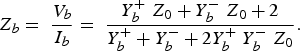 $$Z_b=\; \displaystyle{{V_b } \over {I_b }}=\; \displaystyle{{Y_b^+\; Z_0+Y_b^ - \; Z_0+2} \over {Y_b^++ Y_b^ -+2Y_b^+\; Y_b^ - \; Z_0 }}.$$
The reflection coefficient at input and output ports is given by:
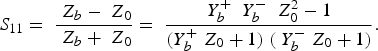 $$S_{11}=\; \displaystyle{{\; Z_b - \; Z_0 } \over {\; Z_b+\; Z_0 }}=\; \displaystyle{{Y_b^+\; \; Y_b^ - \; \; Z_0^2 - 1} \over {\lpar Y_b^+\; Z_0+1\rpar \; \lpar \; Y_b^ - \; Z_0+1\rpar }}.$$
In order to calculate the transmission coefficient, we consider the two ports networks properties, where V 1 is the voltage at the port 1 and V 2 is the voltage at the port 2, and we obtain:
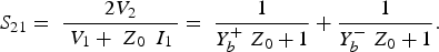 $$S_{21}=\; \displaystyle{{2 V_2 } \over {\; V_1+\; Z_{0\; } \; I_{1\; } }}=\; \displaystyle{1 \over {Y_b^+\; Z_0+1}}+\displaystyle{1 \over {Y_b^ - \; Z_0+1}}.$$
Defining the following functions:
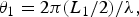 $$\theta_1 =2\pi \lpar L_1 /2\rpar /\lambda\comma \;$$
 $$\theta _2 = 2\pi \lpar L_2 /2\rpar /\lambda\comma \;$$
 $$\theta _a = 2\pi \, L_a /\lambda\comma \;$$
 $$\theta _s = 2\pi \, L_s /\lambda\comma \;$$
 $$G_1 = \; C_2 \, Z_{c\; } \cos \, \lpar \theta _a+\; \theta _s \rpar +j\, A_2 \sin \, \lpar \theta _a+\; \theta _s \rpar \comma \;$$
 $$G_2 = D_2 \, Z_c \cos \, \lpar \theta _a+\; \theta _s \rpar +j\, B_2 \sin \, \lpar \theta _a+\; \theta _s \rpar \comma \;$$
 $$G_3 = Z_c^2 \cos ^2 \lpar \theta _s \rpar \lpar A_{2\; } D_2 - B_2 C_2 \rpar \comma \;$$
 $$G_4 = Z_c \cos \, \lpar \theta _s \rpar \lsqb A_{2\; } \cos \, \lpar \theta _a \rpar +j\, Z_c C_2 \sin \, \lpar \theta _a \rpar \rsqb \comma \;$$
 $$G_1^ + = -j\, Z_c \cot \, \lpar \theta _1 \rpar \comma \;$$
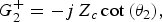 $$G_2^+ = - j\, Z_c \cot \, \lpar \theta _2 \rpar \comma \;$$
 $$G_1^{-} = j\, Z_c \tan \lpar \theta _1 \rpar \comma \;$$
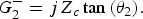 $$G_2^{-} = j Z_c \tan \, \lpar \theta _2 \rpar.$$
We can express Y b+ and Y b− in a compact form:
 $$Y_b^ +=\; \displaystyle{{A_{1\; }+\; C_{1 } G_1^+} \over {B_{1\; }+\; D_{1\; } G_1^+}}+\displaystyle{{G_1 } \over {G_2 - \lpar G_3 /\lpar G_4+G_1 G_2^+\rpar \rpar }}\comma \;$$
 $$Y_b^ -=\; \displaystyle{{A_{1\; }+\; C_{1 } G_1^ - } \over {B_{1\; }+\; D_{1\; } G_1^ - }}+\displaystyle{{G_1 } \over {G_2 - \lpar G_3 /\lpar G_4+G_1 G_2^ - \rpar \rpar }}.$$
A signal passing through the circuit goes out from it with an absolute phase shift in degree given by (19).
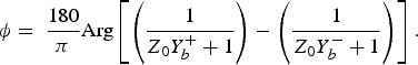 $$\phi=\; \displaystyle{{180} \over \pi }{\rm Arg}\left[{\left({\displaystyle{1 \over {Z_0 Y_b^++ 1}}} \right)- \left({\displaystyle{1 \over {Z_0 Y_b^ -+1}}} \right)} \right].$$
The RL that occurs at the input and output ports is given by (20).
 $$RL=\; - 20{\rm \; log}_{10\; \; } \left\vert {\displaystyle{{Y_b^+\; \; Y_b^ - \; \; Z_0^2 - 1} \over {\lpar Y_b^+\; Z_0+1\rpar \; \lpar \; Y_b^ - \; Z_0+1\rpar }}} \right\vert.$$
The SL TTD has two operative states: the reference state, in which the signal flows through the reference path, and the delay state, in which the signal flows through the delay path. The SPSTs must be identical. Only the state of the switches determines where the signal flows: in the reference state SPST1 are ON and SPST2 are OFF and we have: A 1 = A on, B 1 = B on, C 1 = C on, D 1 = D on and A 2 = A off, B 2 = B off, C 2 = C off, D 2 = D off. In the delay state, SPST1 are OFF and SPST2 are ON and we have: A 1 = A off, B 1 = B off, C 1 = C off, D 1 = D off and A 2 = A on, B 2 = B on, C 2 = C on, D 2 = D on. So we get double formulas: in the reference state we have: Y b ref+, Y b ref−, ϕ ref and RL ref and in the delay state we have: Y b delay+, Y b delay−, ϕ delay and RL delay.
By considering a single angular frequency ω and a non-dispersive medium, for a TEM line with effective dielectric constant ε eff and length L, we have a group delay given by:
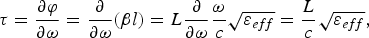 $$\tau=\displaystyle{{\partial \varphi } \over {\partial \omega }}=\displaystyle{\partial \over {\partial \omega }}\lpar \beta l\rpar =L\displaystyle{\partial \over {\partial \omega }}\displaystyle{\omega \over c}\sqrt {\varepsilon _{eff} }=\displaystyle{L \over c}\sqrt {\varepsilon _{eff} }\comma \;$$
where c is the speed of the light in the vacuum. Then we can express the absolute phase shift in radians as a function of this delay in seconds and of the frequency in Hertz as in (22).
 $$\varphi=\beta l=L\displaystyle{{2\pi } \over \lambda }=L\displaystyle{{2\pi } \over c}f\sqrt {\varepsilon _{eff} }=2\pi \cdot f\tau.$$
Given a certain differential group delay, between the two states, as a requirement for a TTD network, this can be transformed in a differential phase shift requirement using:
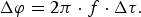 $$\Delta \varphi=2\pi \cdot f \cdot \Delta \tau.$$
Thus, the differential phase shift of a TTD network can be defined as in (24) and the differential group delay is given by (25) which we can express as in (26).
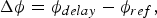 $$\Delta \phi=\phi _{delay} -\phi _{ref}\comma \;$$
 $$\Delta \tau=\tau _{delay} -\tau _{ref}=\Delta \phi /\lpar 2\pi f\rpar \comma \;$$
 $$\eqalign{& \Delta \tau = \displaystyle{1 \over {2\pi\; f}} \cdot \arg \left[ {\displaystyle{1 \over {{Z_0} \cdot Y_{bdelay}^ + + 1}} + \displaystyle{1 \over {{Z_0} \cdot Y_{bdelay}^ - + 1}}} \right] \cr & - \displaystyle{1 \over {2\pi \;f}} \cdot \arg \left[ {\displaystyle{1 \over {{Z_0} \cdot Y_{bref}^ + + 1}} + \displaystyle{1 \over {{Z_0} \cdot Y_{bref}^ - + 1}}} \right].}$$
Otherwise, by given an absolute phase shift in the reference state ϕ ref in degree at single frequency f, as a design requirement, its related delay in seconds is given by (27) and, in the delay state we would have a delay given by (28).
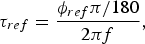 $$\tau _{ref} = \displaystyle{\phi_{ref} \pi / 180 \over 2 \pi f}\comma \;$$
 $$\tau _{delay} = \tau_{ref} + \Delta \tau.$$
Converting this delay in a phase shift, we obtain it in degree given by (29) and, by given an absolute phase shift in the reference state in radians, the design formula with which to obtain the desired differential group delay is given by (30).
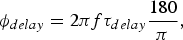 $$\phi_{delay} = 2 \pi f \tau_{delay} \displaystyle{180 \over \pi}\comma \;$$
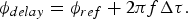 $$\phi _{delay} = \phi _{ref} + 2\pi f \Delta \tau.$$
III. DESIGN METHOD
The proposed design method is based on the numerical resolution of the equation shown before. We use a computer with a mathematical simulator including a numerical solving algorithm, where to implement a series of definitions and conditions whereby to obtain the values of the electrical lengths of the transmission lines which compose the circuit.
A) Characterization of the switches
The first step consists of retrieve information on the switches to be used. To obtain the ABCD parameters of the switches, perform an S-parameters measure with a vector network analyzer (VNA), interpolate the values and create a simulation model to be inserted into an electronic simulator. Then, on the simulator, add to the port of the model some lines of negative length equal to the length of the lines used to connect the real switch ports to the probes of the VNA to de-embed the model. Perform an S-parameters simulation with a large frequency sweep to create a report of the de-embedded S-parameters. Convert these in ABCD parameters using the classical conversion formulas.
B) Dimensioning of the reference line
In order to generate a potentially good matched circuit, it is appropriate to force the reflection coefficient of the total structure to reside in an arc of a circle identified by the intersection of the area included in the circle at desired maximum constant module of the reflection coefficient and the circle with unitary resistance or admittance, imposing a condition on the minimum RL acceptable RL min given by (31) and a condition on real part of the input (or output) impedance Z b or admittance Y b given by (32) and (33).
 $$- 20 \log \left\vert S_{11} \right\vert \geq RL_{min}\comma \;$$
 $${\rm Re}\lpar Z_b \rpar = 1\comma \;$$
 $${\rm Re}\lpar Y_b \rpar =1.$$
In this way, the circuit will be matched using only an inductive or capacitive element.
1) CONDITION OF DIRECT CONNECTION
This is the condition in which the switches are directly connected, we analyze it to know whether to use the formula (32) or (33) in the calculation of the length of the reference line. In the condition of direct connection we can see where, on the smith chart, the S 11 parameter tends to stay. Connecting directly the switches, we assume a circuit in which all the lines have null length. In this case, the forms of indetermination, due to the null lengths of the lines, must be removed in the formulas of Y b+ and Y b−, which become:
 $$Y_b^{+} = \displaystyle{C_{1} \over D_{1}} + \displaystyle{G_1 \over G_2}\comma \;$$
 $$Y_b^{-} = \displaystyle{A_1 \over B_1} + \displaystyle{G_1 \over G_2 - \lpar G_3 /G_4 \rpar}.$$
On a mathematical simulator, using analytical solver, define the values of Z 0, the central frequency f, the null condition on the length of the lines: θ 1 = 0, θ 2 = 0, θ a = 0, θ s = 0, the values of the ABCD parameters of the switches in the delay or reference state, that is the same in this case; insert (34), (35), (9), (10), (11), (12), and (3); then solve the system to find the value of S 11 and see the sign of its real part. If Re(S 11) > 0 the condition to use is (32) and if Re(S 11) < 0 the condition to use is (33).
2) CONDITION OF NULL DIFFERENTIAL PHASE SHIFT
This is the limit condition in which the return losses in the two operative states are equals. If the switches were ideal, then there would be infinite insulation in interdiction state and null insertion loss in conduction state, thus the two paths of the TTD would be completely independent, and the length of the reference line could be set respecting the requirement on the minimum RL in only one state.
As the switches are not ideal, we can find the condition in which the figures of merit of the circuit such as RL and ϕ are more equal as possible in the two operative states.
The limit condition where this happens is the one in which both paths are equal; in this case, the difference of RL in reference and delay states and the differential phase shift are null. In this condition, the lines L a and the stubs L s have null length, which generates forms of indetermination, to be removed in the formulas of Y b+ and Y b−, which become:
 $$Y_b^ +=\; \displaystyle{{A_{1\; }+\; C_{1 } G_1^+} \over {B_{1\; }+\; D_{1 } G_1^+}}+\displaystyle{{A_{2\; }+\; C_{2 } G_1^+} \over {B_{2\; }+\; D_\; G_1^+}}\comma \;$$
 $$Y_b^ -=\; \displaystyle{{A_{1\; }+\; C_{1 } G_1^ - } \over {B_{1\; }+\; D_{1 } G_1^ - }}+\displaystyle{{A_{2\; }+\; C_{2 } G_1^ - } \over {B_{2\; }+\; D_\; G_1^ - }}.$$
3) CALCULATION OF THE ELECTRICAL LENGTH OF THE REFERENCE LINE
For this operation we cannot obtain an exact solution, but we can obtain an optimum solution using a numeric solving algorithm. To do this, we must define the value around which to seek the solution of the system that will be calculated only at the center frequency f.
On a mathematical simulator, using a numerical solver, define the values of Z c, Z 0, and f, the ABCD parameters of the switches in the delay or reference state, and then insert (13), (15), (36), (37), (20), the (32), or (33) depending on the position of S 11 in condition of the direct connection, and insert the inequality (31). At this point, insert the value around which to seek the electrical length of the reference line, for example θ 1 = 1 to obtain a short line, and solve numerically to find it. Then calculate the value of ϕ to use as ϕ ref in the dimensioning of the other transmission lines which compose the rest of the circuit. The physical length of an ideal lossless TEM reference line, remembering that θ 1 is the electrical length of a half reference line, can be calculated by (38).
 $$L_1 = 2 \theta_1 /\beta \; \comma \; \quad {\rm where}\quad \beta = \displaystyle{2 \pi \over c} f \sqrt{\varepsilon _{eff}}.$$
C) Dimensioning of the delay path
Once the reference line has been dimensioned, we can express all the lengths of the other lines as functions of the length of the reference line, by normalizing these ones, using some parameters of proportionality: α 2, α a, α s as follows:
 $$L_2 = 2 \theta_2 /\beta\comma \;$$
 $$L_a = \theta_a /\beta\comma \;$$
 $$L_s = \theta_s /\beta\comma \;$$
 $$\alpha _2 = \theta _2 /\theta _1\comma \;$$
 $$\alpha _a = \theta _a /\lpar 2\theta _1 \rpar \comma \;$$
 $$\alpha _s = \theta _s /\lpar 2\theta _1 \rpar.$$
Note that θ 1 and θ 2 are referred to the half lengths of lines 1 and 2.
1) FEASIBILITY CONSTRAINTS
Feasibility constraints consist of the initial values around which to numerically seek the system solution, in this way we force the algorithm to solve the dimensioning problem around these values, ensuring the layout feasibility. It should be consider the possible spatial positioning of the components that allows the layout physical feasibility, giving to it a geometrically regular shape, typically square or rectangular. The two simplest rectangular examples are represented in Fig. 6. However, more configurations of layout may be used, including bended and meandered lines.
Fig. 6. Examples of rectangular layout configuration: the transmission lines are black-white and the switches are orange-yellow.
By arbitrarily assuming a particular geometric form, we are able to define a coarse combination of the values of α 2, α a, and α s. These coarse values may be rectified to ensure the constant delay and a good matching behavior. In other words, the user needs to suppose a possible combination of these three parameters, by on turn supposing a desired geometrical shape for the circuit. Once we have fixed the reference line, if we would obtain a physical circuit with the shape reported in the left image of Fig. 6, we can chose for example α 2 = 0.7, α a = 0.15, and α s = 0.6. Or we can use α 2 = 1, α a = 0.4, and α s = 0.15, if we would obtain a circuit similar to the right image of Fig. 6. These combinations of three values will be employed order to investigate the behavior of the system as described below. Furthermore, an automatic code can be written in order to suppose the possible combination of these coarse values.
2) TECHNICAL INVESTIGATION
The technical investigation is the procedure whereby we can determine the permitted values of the parameters α 2, α a, and α s, which ensure the constant delay and a good matching behavior of the circuit.
The constant delay is observable when Δϕ is linearly dependent to the frequency, monotonously ascending or descending. It consists in setting two of the three parameters of proportionality and varying the remaining and the frequency too, to obtain two tridimensional graphs of RL ref and RL delay, and a graph of Δϕ as functions of the frequency, where identify the region where the permitted values reside. Briefly we can say that, in the previous step, the user have selected a combination of the coarse values of α 2, α a, α s by an human choice, now he need to maintain two of these three parameter as he have fixed and an automatic program vary the remaining parameter showing the IL and RL of the system.
By performing this operation for all three parameters, we can get an idea about what values to assign to the proportionality parameters, around which to numerically seek the system solution in the calculation of the electrical lengths of the transmission lines which compose the delay path. An example of these graphs is represented in Fig. 7.
Fig. 7. Example of S 11 in reference and delay states and Δϕ versus f. In this case, there is a matching better than 18 dB for 1 < α 2 < 2 and TTD behavior for 0 < α 2 < 2, where Δϕ is always monotonously descending in frequency.
On a mathematical simulator, using an analytical solver, define the values of Z 0, Z c, the values of the ABCD parameters of the switches in the delay and reference state, the value of L 1 previously calculated at the central frequency f; insert the parameterized design formulas, as for example from (45) to (54), and then insert the equations from (9) to (16) and the formulas from (17) to (20) both in reference and in delay state and insert (24), all these ones parameterized as vector functions of the frequency and of the parameter of proportionality that sweeping. At this point, solve analytically to find the matrices of RL ref, RL delay, and Δϕ. Then generate its representative graphs, which describe these values as functions of the frequency and of the parameter of proportionality swept. An example of the parameterized formulas is reported below: in this case the two fixed parameters are α a and α s and the sweeping one is α 2; so θ 2 is function of the indexes i and k respectively relating to the frequency and the L 2 line sweeps.
 $$f_i=f_{start}+i\; \displaystyle{{f_{start} - f_{end} } \over {n_f }}\comma \;$$
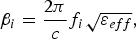 $$\beta_i = \displaystyle{2 \pi \over c}f_i \sqrt{\varepsilon_{eff}}\comma \;$$
 $$\alpha_{2k} = \alpha_{2 start} + k \displaystyle{\alpha_{2 start} - \alpha _{2 end} \over n_\alpha}\comma \;$$
 $$L_{2 k} = \alpha_{2 k} L_1 \comma \;$$
 $$L_a = \alpha_a L_1\comma \;$$
 $$L_s = \alpha_s /L_1\comma \;$$
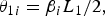 $$\theta_{1 i} = \beta_{i} L_1 /2\comma \;$$
 $$\theta_{2 i\comma \; k} = \beta_i L_{2 k} /2\comma \;$$
 $$\theta_{ai} = \beta_{i} L_a\comma \;$$
 $$\theta_{si} = \beta_i L_s.$$
In the formulas above: f start and f end are respectively the starting and ending value of the frequency sweep, n f is the number of steps in which the frequency axis is divided, and i is the frequency vector index; the same applies to α 2 start, α 2 end, n α, and k.
However, a numerical code can be written to execute automatically both the search of the feasibility constraints and the technical investigation, using as weight function a combination of the values of α 2, α a, and α s to be minimize. In this case, appropriate bonds are to be inserted in order to ensure the feasibility. For example, if we chose the shape reported in the right image of Fig. 6, must be α 2 = 1, 0.1 < α a < 0.5, and 0.1 < α s < 0.5.
The code can be written in order to select these bonds since the user have chosen the desired shape. The full automated program will search for the possible combinations which satisfy the conditions on the maximum RL and minimum IL chosen by the user, and it stops choosing the combination with the minimum area covered by the hypothetical circuit. This can be done by manipulating the values of the resulting α 2, α a, and α s for each iteration.
3) CALCULATION OF THE ELECTRICAL LENGTHS OF THE DELAY PATH
Once the reference line has been dimensioned to have optimum matching condition in reference state, and the parameters of proportionality has been selected to ensure the layout feasibility and rectified to ensure good matching and TTD behavior, we can proceed to design the delay path. As for the calculation of the electrical length of the reference line, for this operation we cannot obtain an exact solution, because the system to solve is non-analytically solvable, but we can obtain an optimum solution using a numeric solving algorithm.
On a mathematical simulator, using a numerical solver, define the values of Z 0, Z c, the values of the ABCD parameters of the switches in the delay and reference state, the value of θ 1 and ϕ ref previously calculated, the value of the desired Δτ, the central frequency f, the values of the three fine proportionality parameters around which to seek the solution, evaluated during the technical investigation; then insert the formulas from (6) to (8), and from (9) to (20) in reference and in delay state; insert (30), (24), and (31).
At this point, solve numerically to find the combination of the correct three values of α 2, α a, and α s, which ensures the desired Δτ with an RL delay less than the maximum specified. Perform the same solving operation using the 360° complement of the angle Δϕ too, by summing 360 in (24). Then, perform an analytic calculation of RL and Δτ inserting the found values of θ 1, α 2, α a, and α s to see the in band performance of the circuit, using the same algorithm used for the technical investigation with no parameter sweeping; only sweeping the frequency we obtain the two dimensional graph of the RL and Δϕ.
All the described system can be fully automated, by linking all the design steps for which all required formulas have been provided. Furthermore, in this chapter we have shown the single-frequency implementation of the proposed formulas, by which circuit sizing starts considering the S-parameters of the switches.
This approach can be extended to a more complex but fine algorithm expanded to the all the desired bandwidth by automating the described technique for all the frequencies for which the SPST's are characterized. For example, in a numerical ambient, a “for” cycle can be employed in order to sweep all the frequencies referring to the desired delay.
IV. APPLICATION: A MONOLITHIC GaAs X-BAND SL TTD
A monolithic 3-bit X-band modified SL TTD network has been designed at the center frequency of 9.6 GHz. Using the proposed technique, electrical lengths of ideal lossless TEM transmission lines have been dimensioned in order to obtain a high-performance circuit starting from the ABCD parameters of the available switches.
The computer program we have described has been written on MATHCAD and, using this mathematical simulator, the ideal lines that compose the circuit have been designed then, on an electronic simulator, have been implemented using microstrip line sections and lumped elements on a GaAs substrate.
This model has been created by fitting the S-parameters curves in frequency on the smith chart of each ideal sized line. Described migration from ideal lines to lumped elements has been performed on AWR MW Office. The ideal transmission lines circuit, computed by the custom mathematic code, has been drawn in AWR and their S 11 and S 21 have been plotted in the operating bandwidth. Lumped circuit has been manually designed in order to fit these plots. Open circuit stubs have been realized by employing short circuit closed capacitors. Transmission lines have been obtained by using shunt capacitors and series inductor π-networks. Values of the lumped elements have been tuned in order to have the same response on the smith chart. Numerical computed transmission lines, implemented on the circuital simulator, had a very long electrical length but with the desired rectangular shape, therefore it was necessary to implement those using lumped elements and line sections. The aim of the transfer from numerical computed ideal circuit to the circuital model was to keep the good IL and RL reducing size while maintaining the rectangular shape.
The circuit uses individual SPSTs which consist of two Depletion FETs based on the technology Selex GaAs pHEMT E/D with 0.4 µm of channel length and 60 µm of channel width, disposed as shown in Fig. 8, in which the series element has four fingers and the shunt element one finger.
Fig. 8. Configuration of the SPST switch.
The proposed circuit operates from 8.1 to 11.1 GHz and consists of three bit TTD element of 15, 30, and 60 ps delay which operates in eight operative states, providing a differential delay from 0 to 105 ps in steps of 15 ps. The chip size is 5 × 2 mm2 and presents a maximum insertion loss of 7.5 dB and minimum RL of 20 dB.
The circuit layout is shown in Fig. 9. Simulated performances of the proposed device are summarized in Table 1; the simulations of the reflection S-parameter and the relative delay versus frequency in each state are respectively shown in Figs 10 and 11. Phase shifts are represented in Fig. 12; relative and absolute transmission S-parameters are shown respectively in Figs 13 and 14.
Fig. 9. The SL TTD layout.
Fig. 10. Reflection parameters.
Fig. 11. Relative delays.
Fig. 12. Phase shifts.
Fig. 13. Relative transmission parameters.
Fig. 14. Absolute transmission parameters.
Table 1. Simulated circuit properties.
We report for comparison, a brief description of two of the most performing recent GaAs MMIC-based TTD networks, found in literature. The 6-bit device presented in [Reference Willms, Ouacha, De Boer and Van Vliet20] operates from 2 to 20 GHz, providing a delay from 2.5 to 145 ps. Even if the total area is 4.0 × 1.4 mm2, the maximum IL is 25 dB and RL is not reported. Another example is described in [Reference Choi, Cho, Bae and Kim21]. This is a 5-bit TTD circuit with a delay from 3.3 to 106 ps operating at 5–20 GHz. The chip size is 1.04 × 0.85 mm2, but presents a maximum insertion loss of 27 dB and minimum RL of 12 dB.
Since the simulation has been performed in a factory provided ambient, by employing the library of transistors, microstrips, lumped elements, and substrate provided by the Selex foundry, we can consider these result with a nice grade of reliability.
V. CONCLUSION
The Modified SL TTD Network Topology has been studied and the formulas that describe its electrical behavior have been derived. To obtain wide band and good matched devices, a design technique, based on technical choices and on the numerical resolution of systems of these equations, has been developed and proposed, and a computer program, which it does, has been implemented on a mathematical simulator.
By employing the proposed technique, the reader might obtain a transmission line based circuit by implementing the reported formulas in a calculator, in which insert the design requirements, the parameters of the switches, and the parameter which describes the desired shape of the device, referring, for example, on the antenna to be use.
This results in achieving optimal performance and much project time saving, as we have documented in this paper. A monolithic 3-bit X-band modified SL TTD from 0 to 105 ps at the center frequency of 9.6 GHz has been designed with great performance: 30% of overall operative band with an RL greater of 20 dB in 10 mm2 of area.
 Alberto Leggieri received his degree in Electronic Engineering in 2011 from the University of Rome “Tor Vergata”. Now, he is with S.I.T. S.p.A as R&D R.F. Engineer and R.F. Laboratory Manager in developing IORT dedicated electron accelerators, and he is attending the Ph.D. course in Electronic Engineering in developing High Power Microwave devices such as Power Spatial Combiners, Electron Guns, LINAC, Magnetrons, and Vircators. He upgraded the accelerating structures and designed several Electromagnetic and RF-MW devices of the mobile e-IORT accelerators LIAC and LIAC-S. His research interests are in applied electromagnetism, MMIC devices, Vacuum Tubes, LINAC, and Multiphysics Modeling.
 Davide Passi received his degree in Electronic Engineering in July 2013 from the University of Rome “Tor Vergata”. Now, he is attending the Ph.D. course in Electronic Engineering in developing High, Medium Power, and passive Microwave devices such as Power Spatial Combiners and Power amplifiers. He designed several Spatial Power Combining Amplifiers in collaboration with Elettronica S.p.A. His research interests are in Applied Electromagnetism, MMIC devices, and Solid State Microwave Power Amplifier.
 Franco Di Paolo received his Ph.D. degree in Electronic Engineering in 1984 from the University of Rome “La Sapienza”. He has spent several years as microwave circuit designer in industries as Fatme-Ericsson S.p.A, Elettronica S.p.A, Telit S.p.A, and Finmek-Space S.p.A. Now, he is with the University of Roma “Tor Vergata”, Italy. His research interests are in Applied Electromagnetism, Solid State Microwave Power Amplifier, and Vacuum Tube Microwave Power Amplifiers. He is an IEEE Associate Member of CAS and MTT Societies.


