


I. INTRODUCTION
Microstrip patch antennas have been designed and characterized extensively over the past many years because of their low-profile structures, light weights, and low cost in fabrication [Reference Zhao, Li and Xiao1–Reference Yuan, Yeo, Nie and Li8] where various design techniques and fast solvers have been developed to enhance radiation performance (such as bandwidth and gain). These low-profile antennas are useful in aircraft, satellite, and missile applications where size, weight, cost, performance, ease of installation, and aerodynamic profiles are strict constraints. In spite of many advantages, these antennas suffer from some disadvantages which include their low efficiency, low power, high Q, spurious feed radiation, and very narrow bandwidth [Reference Moradi and Nikmehr9–Reference Asimakis, Karanasiou and Uzunoglu14]. There have been considerable efforts made by researchers from all over the world toward increasing its bandwidth. A possible way for increasing the bandwidth is to either increase the height of the dielectric or decrease the dielectric constant. However, the first approach would make it unsuitable for low-profile structures, whereas the latter approach will make the matching circuit to the patch difficult due to excessively wide feeding lines. Various other techniques [Reference Shakelford, Lee, Chatterjee, Guo, Luk and Chair15–Reference Anguera, Puente and Borja17] have been proposed to increase the bandwidth of a patch antenna. Bandwidth of small size microstrip antennas has been improved by the use of U slot and L probe [Reference Shakelford, Lee, Chatterjee, Guo, Luk and Chair15], stacked microstrip patch antenna [Reference Lee, Lee and Bobinchak16–Reference Anguera, Font, Puente, Borja and Soler18], aperture coupled, and impedance matching network using filter design techniques [Reference Pues and Van De Capelle19, Reference Slavova, Abdel Rahman and Omar20], unbalanced structures [Reference Li, Ooa and Li21].
Another way of increasing the bandwidth of the MPA is the use of additional resonators either directly or indirectly coupled to the patch antenna [Reference Abdelaziz22].
The use of electromagnetic band gap (EBG) structures for improving the characteristics of MPA such as improving their radiation patterns, enhancing their gain, and minimizing the side and back lobe levels, etc. has attracted much attention among researchers in the microwave and antenna communities [Reference Yang and Rahmat-Samii23]. Various EBG structures have been proposed and they have found many applications in the microwave region [Reference Yang, Fan, Chen, She and Feng24–Reference Yang, Fan and Feng27]. Recently, EBG structure on the feed line has also been studied to improve the performance of a triple-band slot antenna [Reference Xu, Ooi and Zhao28].
The main objective of this paper is to present a new antenna configuration with combined effect of slotting, the use of directly coupled parasitic elements and fractal EBG structures to design a simple low-profile broadband antenna. Fractal structures have shown advantages in designing small, multiband, and high-directive antennas [Reference Anguera, Puente, Borja and Soler29–Reference Anguera, Martínez, Puente, Borja and Soler32]. Firstly, slotting was done by introducing four slits on all the four sides of a rectangular-shaped patch antenna as shown in Fig. 1. Then four different radiating elements connected together and directly coupled to the slotted antenna as shown in Fig. 2 were added, which shows an improvement in bandwidth from 9.3 to 18%. Later on by embedding fractal EBG structures in the same antenna it was being observed that the bandwidth was increased upto 23.7%. A comparative analysis was also done at different heights of fractal EBG structures. The material used as the substrate is FR4 (glass epoxy, ɛr = 4.4) and the type of feed used is coaxial probe feed. The simulation is done using HFSS, which is based on finite-element method (FEM).

Fig. 1. Top view of slotted patch antenna.

Fig. 2. Top view of slotted patch antenna with directly coupled parasitic elements.
II. ANTENNA DESIGN
A) Slotted rectangular microstrip patch antenna
In this section, a slotted patch antenna is designed. Figure 1 depicts the geometry of the proposed patch antenna with its dimensions 36 × 28 mm. The four slits, as shown in Fig. 1, are created in its shape. The FR4 material is used as the substrate whose thickness is 3.2 mm (h1) (Fig. 3). The dimensions of the slits along the length are L1 = 4 mm and W1 = 10 mm and along the width are W2 = 4 mm and L2 = 12 mm. The feed is positioned 0.6 mm along the x-axis and 4.3 mm along the y-axis from the center of the rectangular patch. The ground plane size is 100 × 100 mm. The proposed antenna is simulated using HFSS, which is based on FEM. Figure 4 shows the simulated impedance bandwidth. The impedance bandwidth is found to be 9.3% ranging from 4.2 to 4.61 GHz. By embedding the suitable slits in the radiating patch, compact operation with an enhanced impedance bandwidth is obtained [Reference Wong33].
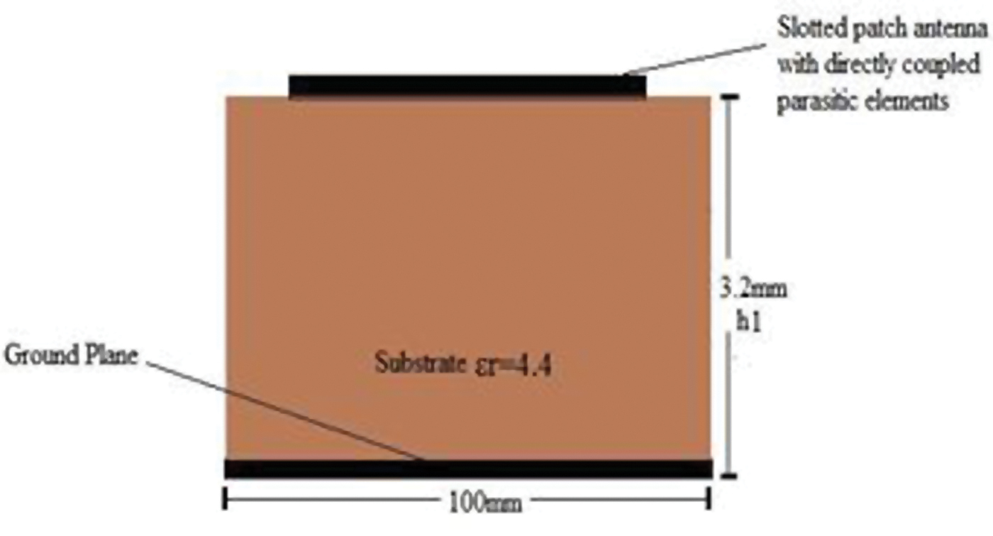
Fig. 3. Side view of slotted patch antenna with directly coupled parasitic elements.

Fig. 4. Reflection coefficient (in dB) versus frequency (in GHz) for slotted patch antenna shown in Fig. 1.
B) Bandwidth improvement by the use of directly coupled parasitic elements
The antenna designed in Section A still has narrow bandwidth by seeing the demand for overgrowing need of wireless communication. The second technique employed here to increase its bandwidth is the use of directly coupled parasitic elements. Figure 2 shows the geometry of the proposed new modified slotted patch antenna with parasitic patches. These additional resonators generate the modes very close to the fundamental resonant frequency of the main patch resulting in broad bandwidth. As shown in the figure, additional parasitic elements are directly coupled and inserted in the slits of the slotted patch antenna. All the dimensions of the parasitic elements are shown in Fig. 2. This new antenna with parasitic elements has bandwidth of 18%, which is twice that of the slotted patch antenna. This antenna operates in the range of 3.53–4.23 GHz. The length and width of each element of these parasitic elements are optimized to get the broad bandwidth. The optimized feed location is found to be at 0.62 mm along the x-axis and 4.3 mm along the y-axis from the center of the rectangular patch. The results are shown in Fig. 5.

Fig. 5. Reflection coefficient (in dB) versus frequency (in GHz) for slotted patch antenna with directly coupled parasitic elements shown in Fig. 3.
C) New modified antenna design using fractal EBG structures for wide bandwidth
In this section, a third technique is employed to further improve the bandwidth of the antenna designed in Section B. By the use of EBG structures the characteristics of the patch antenna can further be enhanced. An EBG structure is a periodic structure that forbids the propagation of all electromagnetic waves within a particular frequency band called the band gap. The performance improvement occurs due to the stop bands of these periodic structures. These structures provide a simple and effective solution to surface and leaky waves. Several types of microstrip based EBG structures have been analyzed for a variety of applications.
Figure 6 shows the geometry of the single element of the EBG structures. An array of 6 × 6 EBG structures is embedded at a height of 1.6 mm (h2) as shown in Fig. 7 and Fig. 8. Each single-array element has dimensions of L7 = 12 mm and W7 = 12 mm as shown in the figure. The gap between the array elements, L5 = 4 mm and W5 = 4 mm is also shown in the figure. This new modified antenna design using EBG structures has a wide bandwidth of 23.7% ranging from 4.15 to 5.27 GHz as shown in Fig. 9 in comparison to 18% of the antenna designed in Section B. The antenna is found to resonate at the frequency of 4.17 GHz with −38.60 dB reflection coefficient.

Fig. 6. Single element of EBG structures.

Fig. 7. 6 × 6 array of EBG structures.

Fig. 8. Side view of the new modified antenna design with EBG structures.
The side view of the new modified antenna design is shown in Fig. 8. The EBG structures were embedded at the height of 1.6 mm (h2) from the ground plane in the antenna designed in Section B. The modified feed location is found to be at 0.6 mm along the x-axis and 4.6 mm along the y-axis from the center of the rectangular patch.

Fig. 9. Reflection coefficient (in dB) versus frequency (in GHz) for slotted patch antenna with directly coupled parasitic elements and embedded fractal EBG structures shown in Fig. 6.
D) Simulated results and discussion
1) SLOTTED PATCH ANTENNA
Figure 4 shows the reflection coefficient curve for the antenna designed in Section A. The simulated results show that the resonant frequency locates at about 4.31 GHz with the maximum reflection coefficient of −33.55 dB. The −10 dB impedance bandwidth is found to be 9.3% ranging from 4.2 to 4.61 GHz.
2) SLOTTED PATCH ANTENNA WITH DIRECTLY COUPLED PARASITIC ELEMENTS
The result in Section A shows only the limited bandwidth. To further enhance the bandwidth of the patch antenna designed in Section A, the use of parasitic elements is made which increased the bandwidth to 18% ranging from 3.53 to 4.23 GHz. Figure 5 shows the reflection coefficient curve for the antenna designed in Section B. The maximum reflection coefficient is found to be −29.12 dB located at the resonant frequency of 3.63 GHz.
3) NEW MODIFIED ANTENNA WITH EMBEDDED FRACTAL EBG STRUCTURES
Figure 9 shows the reflection coefficient curve for the antenna designed in Section C. By embedding the fractal EBG structures the bandwidth was further improved to 23.7% ranging from 4.15 to 5.27 GHz. It is being observed from the figure that by embedding EBG structures the bandwidth is drastically improved.
4) EFFECT OF EMBEDDING FRACTAL EBG STRUCTURES AT DIFFERENT HEIGHTS FROM GROUND PLANE
Figure 10 shows the reflection coefficient curve of the new proposed antenna with EBG structures at different heights. The height from the ground plane of the EBG structures is optimized to get the broad bandwidth. The optimum result is found at height h2 = 1.6 mm from the ground plane as can be seen in Fig. 8.

Fig. 10. Effect of fractal EBG structures at different heights from ground plane.
Figure 11 shows the radiation pattern for slotted patch antenna with directly coupled parasitic elements and embedded fractal EBG structures at height h2 = 1.6 mm. The main beams are in the broadside direction of the antenna. The radiated power degrades in the off-axis direction.

Fig. 11. Radiation pattern for slotted patch antenna with directly coupled parasitic elements and embedded fractal EBG structures (a) 4.18 GHz, (b) 5.18 GHz.
III. CONCLUSION
In this paper a very wideband patch antenna is designed, employing the three techniques of slotting, adding directly coupled parasitic elements, and embedding fractal EBG structures. From the simulation result it is being observed that by adding slots in the normal rectangular-shaped patch antenna the bandwidth is 9.3% .This bandwidth is further improved to 18% by adding directly coupled parasitic elements, which is just twice to that of the slotted antenna. To further increase the bandwidth the third feature is incorporated that is the use of 6 × 6 fractal EBG structures. These EBG structures are embedded in the modified patch to increase the bandwidth upto 23.7%. This antenna can be used to provide the wide-band operation for WLAN and radar applications.
ACKNOWLEDGEMENT
We highly acknowledge the authorities of Jaypee Institute of Information Technology, NOIDA for their support in carrying out our work successfully.
 Archana Agrawal is B.E., M.Tech, and pursuing Ph.D. in the field of Electronics and Communication Engineering. She is working as an assistant professor in the Department of Electronics and Communication at ITM Bhilwara and has a total teaching experience of 8.5 years. Her area of interest lies in the field of antenna designing and microwave engineering.
 Pramod Kumar Singhal is B.E., M.Tech, and Ph.D. in the field of Electronics Engineering. Presently, he is working as a professor and head of the Department of Electronics, Madhav Institute of Technology and Science, Gwalior. He is also working as a chief coordinator of research projects sponsored by the Department of Science and Technology, Govt. of India and All India for Technical Education, New Delhi, and has a teaching experience of more than 20 years. His area of interest lies in the field of antenna designing and microwave engineering.
 Ankit Jain is B.Tech in Electronics and Communication from Jaypee Institute of Information Technology, Noida. His areas of interest are Antennas Designing, Wireless Communication.


