


Introduction
The current trend for millimeter-wave (MMW) wireless communication systems is toward high integration and high flexibility, which has led to an interest in developing multi-band and multi-standard transceivers. Traditional design strategies have adopted separate single-band radio-frequency (RF) front-ends in parallel for multi-band and multi-standard operations, which increase the power consumption and chip size. To alleviate this problem, the RF building blocks which can be shared among multiple frequency bands are highly required [Reference Wolf, Joram, Schumann and Ellinger1–Reference Alqaisy, Chakrabraty, Ali and Alhawari3].
There have been several demonstrations of dual-band mixers. For instance, a 4/8 GHz dual-band up-conversion mixer was proposed by using two mixer cores followed by a combiner [Reference Arasu, Zheng and Yeoh4]. A 2.4/5.7 GHz dual-band Gilbert up-conversion mixer and a 2.45/5.2 GHz dual-band Gilbert down-conversion mixer using dual-band LC matching networks were proposed in [Reference Syu and Meng5] and [Reference Liang, Rao, Huang and Chung6], respectively. By reconfiguring the output waveform of the local oscillator (LO), dual-band mixing can also be achieved [Reference Jackson and Saavedra7, Reference El-Nozahi, Amer, Sánchez-Sinencio and Entesari8]. All these mixers, however, were demonstrated below 12 GHz. Recently, an MMW dual-band switchable star mixer and an MMW fundamental and subharmonic hybrid ring mixer have been proposed in [Reference Wang, Hou, Chen and Hong9,Reference Zhu and Luo10], respectively. However, the passive mixers suffer from high conversion loss and require high LO pumping power, especially in complementary metal oxide semiconductor (CMOS) technologies. An MMW dual-band CMOS down-conversion mixer with a modified Gilbert topology was demonstrated in [Reference Zhu, Wang and Wu11], but the balun-based input stage is not suitable for an up-conversion mixer and the conversion gain is still unsatisfactory.
In this paper, an MMW dual-mode and dual-band switchable Gilbert up-conversion mixer in a commercial 65-nm CMOS process is presented. The proposed CMOS Gilbert up-conversion mixer can be switched between subharmonic and fundamental operation modes by simply changing its bias, and thus is suitable for dual-band applications. This is appealing for 5 G MMW systems to reduce the system size and increase the versatility.
Circuit design
Figure 1 shows the schematic of the proposed MMW dual-mode and dual-band switchable CMOS Gilbert up-conversion mixer. It is composed of three levels of sub-circuits. The lower-level sub-circuit (M 1–M 2) acts as a transconductance stage, which converts the intermediate frequency (IF) input signal to output current. The middle-level sub-circuit (M 3–M 8) is composed of a switching quad (M 3–M 6) and a differential common-gate stage (M 7–M 8). The bias voltages of the switching quad and the differential common-gate stage are provided through two switches, i.e. SW 1 and SW 2, which are controlled by the control voltage V C. The upper-level sub-circuit (M 9–M 12) acts as another switching quad. The two stacked switching quads are driven by two quadrature LO signals, i.e. LOI and LOQ, respectively, which are generated by a 90° coupler and two Marchand baluns [Reference Zhu, Wang and Wu11, Reference Wei, Meng, Wu and Tsung12]. By adding four bypass capacitors (C 4–C 7), the LO baluns could provide dc bias voltages (V A and V G3) for the top and bottom switching quads without affecting the LO characteristics. The up-converted RF differential output signals are directed to a Marchand balun [Reference Tsai and Lin13] for differential to a single output, while the inductors L 1 and L 2 are inserted between the RF balun and the top switching quad for RF impedance matching.
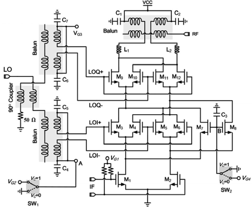
Fig. 1. Schematic of the proposed MMW dual-mode and dual-band switchable CMOS Gilbert up-conversion mixer.
To better understand the operation of the proposed CMOS Gilbert mixer, let us define S 1(t) as the switching function of the middle-level sub-circuit (M 3–M 8), and S 2(t) as the switching function of the upper-level sub-circuit (M 9–M 12). Since the IF current is sequentially multiplied by S 1(t) and S 2(t), the equivalent switching function of the whole circuit can be expressed as S(t) = S 1(t)S 2(t).
When V C = 1 V, the differential common-gate devices M 7–M 8 are in off-state, while the gates of the transistors M 3–M 6 are biased at V G2 (i.e. V A = V G2), which is around the turn-on voltage of the bottom switching quad. In this case, S 1(t) equals to the switching function of the bottom switching quad. On the other hand, S 2(t) equals to the switching function of the top switching quad. Assuming hard switching of the transistors, S 1(t) and S 2(t) can be represented as two square waves aligned with the two LO signals (i.e. LOI and LOQ), as illustrated in Fig. 2(a). Since LOI and LOQ are in quadrature, the switching frequency of S(t) is doubled, as shown in Fig. 2(a). Thus, subharmonic mixing is obtained. Specifically, the whole circuit operates as a Gilbert stacked-LO subharmonic mixer [Reference Sheng, Jensen and Larson14], which has the advantages of high conversion gain and high port-to-port isolation while requiring a low LO pumping power.

Fig. 2. Switching functions of the proposed CMOS Gilbert up-conversion mixer for (a) subharmonic operation mode and (b) fundamental operation mode.
When V C = 0 V, the differential common-gate devices M 7–M 8 are activated, while the gates of the transistors M 3–M 6 are biased at 0 V. The bottom switching quad is in the off-state during both the positive and negative excursions of LOI as long as V LOI < V DT + V TH, where V LOI is the voltage amplitude of LOI, V DT is the drain voltage of the IF transconductance stage, and V TH is the threshold voltage of the transistor. In this case, S 1(t) equals to the switching function of the differential common-gate stage and therefore can be represented as a constant in the time diagram. Therefore, the switching frequency of S(t) equals to that of S 2(t), as shown in Fig. 2(b). Since S 2(t) still equals to the switching function of the top switching quad, fundamental mixing is obtained. In particular, since the lower- and middle-level sub-circuits are acting as a differential cascode amplifier, the conversion gain of the mixer can be improved. It should be noted that the condition V LOI < V DT + V TH is necessary during the operation of the fundamental mode, otherwise, the bottom switching quad will be activated during the positive excursion of LOI and the conversion gain of the mixer would drop rapidly. The simulation indicates that the LO pumping power should be lower than 8 dBm for the operation of fundamental mixing mode.
By exploiting these two distinct mixing modes of operation, the proposed CMOS Gilbert up-conversion mixer can be adopted to cover two different MMW bands for dual-band applications.
For the mixer design, the selection of device size and bias point is critical. Theoretically, larger devices have a higher transconductance and hence should result in a higher conversion gain. However, they also suffer from larger parasitic capacitances and higher dc power consumption. Therefore, a trade-off should be concerned during the device selection. In this design, the gate width is 20 μm for M 3–M 12 and is 40 μm for M 1–M 2. The bias voltages are first investigated to make sure that the devices are in saturation, and then are optimized for each mode to obtain sufficient conversion gain and low dc power consumption. The final bias voltages are V G1 = 0.45 V, V G2 = 0.7 V, V G3 = 0.9 V, and V G4 = V CC = 1 V.
An Agilent ADS corresponding to a Taiwan Semiconductor Manufacturing Company design kit was employed for circuit simulation. The passive structures, including the inductors, capacitors, coupler, and Marchand baluns, were simulated by ADS Momentum, and the whole circuit was simulated by ADS harmonic-balance simulator.
Experimental results
The proposed MMW dual-mode and dual-band switchable Gilbert up-conversion mixer is designed and fabricated in commercial 65-nm CMOS technology. The chip photo is shown in Fig. 3. The chip size is 0.5 mm2, including all pads and dummy metal. The measurements of the circuit are performed via on-wafer probing with 150 μm pitch coplanar ground-signal-ground probes. The input IF signal is generated by a vector signal generator (Agilent E8267D), the LO source is generated by an analog signal generator (Agilent E8257D), and the up-converted RF signal (the upper sideband) is measured by a spectrum analyzer (Agilent N9030A). The insertion losses of the probes and cables were measured by a PNA-X network analyzer (Agilent N5245A) and de-embedded from the measured results. Under 1-V supply voltage, the proposed CMOS Gilbert mixer draws 6 mA of dc current in both subharmonic and fundamental operation modes.

Fig. 3. Chip photo of the proposed CMOS Gilbert up-conversion mixer.
Figure 4 shows the simulated and measured conversion gain of the proposed CMOS Gilbert up-conversion mixer for both subharmonic and fundamental modes versus LO power. The LO frequency is fixed at 24 GHz and the IF frequency at 0.1 GHz. As can be observed, an LO power of 3 dBm is required to achieve a good conversion gain for both subharmonic and fundamental modes. In addition, as expected, the measured conversion gain of the mixer in the fundamental mode drops rapidly when the LO power is higher than 8 dBm. In the following measurements, the LO pumping power (i.e. the output power at the tips of the LO probe) is fixed at 3 dBm. To level the LO power with frequency variation, the insertion losses of the probe and cable on the LO path versus LO frequency, which have been measured by PNA, should be compensated at the output of the LO signal generator.

Fig. 4. Simulated and measured conversion gains versus LO power for both subharmonic and fundamental modes.
Figure 5 shows the simulated and measured IF bandwidth of the proposed CMOS mixer for both operation modes. As can be observed, the IF bandwidth is larger than 2 GHz and 1.5 GHz for the subharmonic and fundamental modes, respectively. Without loss of generality, a single tone with the frequency of 0.1 GHz is used for the IF input signal in the following measurements.

Fig. 5. Simulated and measured IF bandwidth for both subharmonic and fundamental modes.
Figure 6 shows the simulated and measured conversion gains versus RF frequency for both operation modes. The proposed CMOS Gilbert up-conversion mixer exhibits a measured conversion gain of −0.5 ± 1.5 dB from 37 to 50 GHz and 2.5 ± 1.5 dB from 17.5 to 32 GHz for the subharmonic and fundamental modes, respectively. The two operation bands cover the 24.75-27.5 GHz and 37-42.5 GHz bands for 5 G MMW applications.

Fig. 6. Simulated and measured conversion gains for both subharmonic and fundamental modes.
The discrepancy between the simulation and measurement shown in Figures 4–6 is mainly due to the inaccurate modeling of the transistors, non-predictable parasitic effects of the layout, and inaccurate extraction of the effective relative permittivity of the multi-layered substrate. In fact, general device models provided by foundry are not guaranteed above a certain frequency range (e.g. <30 GHz) and do not include the parasitic effects due to the interconnects within the transistors, which can be very significant at MMW frequencies. The pads and lossy substrate also introduce considerable high-frequency parasitic effects. Besides, unwanted coupling effects between neighboring structures are not accurately predicted. Additionally, the inaccurate effective relative permittivity of the multi-layered substrate used in the layout simulation may cause frequency offset between the measured and simulated results.
Figure 7 shows that the measured 2LO-to-RF isolation for the subharmonic mode is higher than 47 dB and the measured LO-to-RF isolation for the fundamental mode is higher than 41 dB, respectively. Figure 8 shows the measured conversion gains for both operation modes versus the IF input power. The output 1 dB power compression point (OP1dB) of the proposed CMOS Gilbert up-conversion mixer is −14.4 and −8.1 dBm for the subharmonic and fundamental modes, respectively. To investigate the linearity of the mixer, an IF two-tone with frequency offset of 10 MHz is generated for the input. Figure 9 shows that the measured output third intercept point (OIP3) of the proposed mixer is −3.9 and 1.2 dBm for the subharmonic and fundamental modes, respectively when the LO frequency is 24 GHz.

Fig. 7. Measured LO-to-RF and 2LO-to-RF isolations.

Fig. 8. Measured conversion gains versus the IF input power for both subharmonic and fundamental modes.

Fig. 9. Measured OIP3 for both subharmonic and fundamental modes.
Table 1 shows the performance of the proposed CMOS Gilbert up-conversion mixer along with several other MMW CMOS subharmonic up-conversion mixer dies. The proposed CMOS Gilbert up-conversion mixer achieves good conversion gain in dual bands and high port-to-port isolation with a low LO pumping power and a low dc power consumption.
Table 1. Comparison of MMW CMOS subharmonic up-conversion mixer dies.

*I/Q Modulator. **With RF buffer. ***Single sideband value.
Conclusion
In this paper, an MMW dual-mode and dual-band switchable Gilbert up-conversion mixer using a commercial 65-nm CMOS process is presented. With a 3-dBm LO power and a 6-mW dc power consumption, the proposed CMOS up-conversion mixer exhibits a conversion gain of −0.5 ± 1.5 dB from 37 to 50 GHz and 2.5 ± 1.5 dB from 17.5 to 32 GHz for the subharmonic and fundamental modes, respectively. Both the 2LO-to-RF and LO-to-RF isolations are higher than 40 dB. The measured OP1dB is −14.4 and −8.1 dBm for the subharmonic and fundamental modes, respectively. Compared with previously reported MMW CMOS subharmonic up-conversion mixers, the proposed CMOS Gilbert up-conversion mixer achieves good conversion gain and isolation performances for dual operation modes and dual frequency bands.
Acknowledgement
This work was supported in part by the Natural Science Foundation of China under Grant 61901147 and in part by the Qianjiang Talent Project Type-D of Zhejiang under Grant QJD1902012.
 Fang Zhu received the B.S. degree in electronics and information engineering from Hangzhou Dianzi University, Hangzhou, China, in 2009, and the M.S. and Ph.D. degrees in electromagnetic field and microwave technique from Southeast University, Nanjing, China, in 2011 and 2014, respectively. From 2014 to 2016, he was a MMIC Designer with Nanjing Milliway Microelectronics Technology Co., Ltd, Nanjing, China. From 2016 to 2019, he was a Postdoctoral Research Fellow with the Poly-Grames Research Center, Polytechnique Montréal, Montréal, QC, Canada. He is currently a Professor with the School of Electronics and Information, Hangzhou Dianzi University, Hangzhou, China. His current research interests include microwave and millimeter-wave integrated circuits, components and transceivers for wireless communication and sensing systems.
 Guo Qing Luo received the B.S. degree from the China University of Geosciences, Wuhan, China, in 2000, the M.S. degree from Northwest Polytechnical University, Xi'an, China, in 2003, and the Ph.D. degree from Southeast University, Nanjing, China, in 2007. Since 2007, he has been a Lecturer with the faculty of School of Electronics and Information, Hangzhou Dianzi University, Hangzhou, China, and was promoted to Professor in 2011. From October 2013 to October 2014, he joined the Department of Electrical, Electronic and Computer Engineering, Heriot-Watt University, Edinburgh, UK, as a Research Associate, where he was involved in developing low profile antennas for UAV applications. He has authored or co-authored over 110 technical papers in refereed journals and conferences and holds 19 patents. His current research interests include RF, microwave and mm-wave passive devices, antennas, and frequency selective surfaces.


