


I. INTRODUCTION
Integrated transformers represent an important component on the design of RF integrated circuits. They have been extensively used as part of wireless transceivers which comply with communications standards operating in frequencies inferior to 10 GHz, such as Wi-Fi, Bluetooth, and Universal Mobile Telecommunications System (UMTS). Some important studies concerning the design and modeling of transformers at those frequencies are included in [Reference Niknejad and Meyer1–Reference El-Gharniti, Kerherve and Begueret4].
More recently, some relevant new applications have emerged in the millimeter-wave (mm-wave) range. Among them, one can mention the high data rate Wireless Personal Area Network (WPAN) and Wireless Local Area Network (WLAN) exploiting the unlicensed band in the vicinity of 60 GHz, the automotive radar at 77 and 79 GHz, and imaging at 94 GHz. At these frequencies, as well, the use of transformers has shown very useful properties [Reference Dickson, LaCroix, Boret, Gloria, Beerkens and Voinigescu5–Reference LaRocca, Liu and Chang8].
Transformers can perform different functions in an integrated circuit. They are frequently employed as a balanced to unbalanced modes conversion element (balun). Their advantage over traditional transmission-line-based structures consists mostly on the lesser surface occupation and their wideband behavior. Transformers are also often included in matching networks within or between circuits in transceivers. They are also known to constitute effective power combiners, which are especially useful for parallel power amplifier topologies, and to perform DC decoupling and be part of feedback and resonant networks.
As aforementioned, the use of transformers for impedance matching may be very interesting in an integrated circuit. In order to accomplish this task as efficiently as possible, it is important that the component provide a suitable impedance transformation from its primary to secondary coil.
Previous works have reported different techniques used to obtain the desired impedance ratios on integrated transformers. For RF transformers operating in lower frequencies, the adopted topology is usually based on multiturn spirals. The transformation ratios are hence obtained through the choice of a convenient turn ratio between primary and secondary. In those cases, the number of turns of a particular winding is generally limited to five [Reference El-Gharniti, Kerherve and Begueret4, Reference Rotella, Cismaru, Tkachenko, Cheng and Zampardi9].
Nevertheless, even for those frequencies, different topologies have been proposed to achieve higher impedance ratios. In [Reference El-Gharniti, Kerherve and Begueret4], for instance, all turns of one of the windings are connected in parallel in order to decrease its overall effective inductance. Lim et al. [Reference Lim10] extrapolate this idea by connecting the different primary turns several times in parallel. Moreover, a multi-layer approach is used to further increase secondary inductances.
At mm-waves, on the other hand, we cannot design transformers with more than two turns in a winding. A superior number of turns would imply a considerably low resonant frequency, so that proper mm-wave operation would not be possible, and higher losses would appear. For this reason, most of the transformers currently used in mm-wave-integrated circuits present stacked single-turn primaries and secondaries so that their inductance ratios are close to 1 [Reference Chowdhury, Reynaert and Niknejad6, Reference Chan, Long, Spirito and Pekarik11]. Hence, they are mostly suited to work as baluns.
Some transformers that perform impedance transformation at mm-waves can be seen in [Reference Dickson, LaCroix, Boret, Gloria, Beerkens and Voinigescu5, Reference LaRocca, Liu and Chang8]. Those transformers present a 1:2 turn ratio and an interleaved topology (primary and secondary implemented on the same metal layer). Additionally, in all those cases, the trace width of primary conductors is the same as that of the secondary. A different approach is presented in [Reference Cheung and Long12]. For this transformer, the primary is placed within the secondary, i.e., the secondary completely encloses the primary both horizontally and vertically. In this case, the primary, which has two turns, presents narrower traces than the single-turn secondary.
In this paper, we propose a novel topology based on a stacked configuration, for which primaries and secondaries present different trace widths and diameters in order to achieve higher transformation ratios for frequencies inferior to 90 GHz in the mm-wave spectrum [Reference Belot, Leite, Kerhervé and Bégueret13]. In Section II, the structure of the transformers is introduced and detailed. Section III reports the characteristics of the technologies that were employed in this study and specifies the adopted model and measurement setup. Finally, Section IV summarizes and discusses the obtained results.
II. TRANSFORMERS DESIGN
Our design employs a stacked topology, as shown in Fig. 1. The primary is implemented on the top copper metal layer available in the technology and the secondary on the layer immediately beneath. This allows the conductors to be as far as possible from the substrate, which reduces the associated capacitance. It also reduces the metallic losses, since, for many current technologies, the two top metal layers are considerably thicker than the others. Also, the choice of a stacked topology permits a smaller surface occupation and a stronger magnetic coupling between windings, as long as metal layers are sufficiently close in the vertical direction – as it is the case for the considered technologies. Moreover, in order to minimize losses, no shield is inserted between the conductors and the substrate [Reference Leite, Kerhervé, Bégueret and Belot14] and the windings present an octagonal shape.

Fig. 1. Layout of stacked transformer with different diameters (D) and trace widths (W).
The proposed topology is based on two well-known principles of transmission lines and lumped inductances. First of all, the longer a line is, the higher its inductance will be. Considering the geometric parameters we adopt in our transformer design, it means that larger diameters will lead to higher inductances. Also, the wider a conductor trace is, the lower its respective inductance will be. Moreover, we also employ the number of turns as a parameter to obtain the desired impedance ratios. An inductor with two turns will present a higher inductance value not only for being electrically longer, but also due to the mutual inductance between turns.
The partial inductance of a conductor can be expressed by equation (1). It depends linearly on the length ℓ, and logarithmically on the width W and thickness t. This expression is derived from a fundamental formula for the mutual inductance between filaments, for which the distance separating them is replaced by the geometric mean distance among the points within a section of the conductor [Reference Grover15], and their length is considered much greater than the other dimensions:
![\eqalign{L\lpar \ell\comma \; W\comma \; t\rpar =\displaystyle{0.42\mu _0 \over \pi }&\ell \left[{\ln \left(\displaystyle{2\ell \over 0.2235\lpar W+t\rpar } \right)}\right. \cr &\left. {\quad+\displaystyle{{0.2235\lpar W+t\rpar } \over \ell } - 1} \right].}](https://static.cambridge.org/binary/version/id/urn:cambridge.org:id:binary:20151130141029191-0042:S1759078711001073_eqn1.gif?pub-status=live)
Hence, we design a transformer presenting its primary and secondary with different conductor widths and different diameters. The dimensions should be comprised between the cases when inner diameters and outer diameters of the windings coincide, so that vertical coupling can take place. The minimum and maximum trace widths, on the other hand, should be determined by metal density rules, which are specific to each technological process.
Therefore, in order to achieve a transformation ratio as high as possible, the primary traces should be made as wide and the secondary traces as narrow as possible. Additionally, the primary must be single turn and the secondary would present two turns. Finally, the outer diameters of the windings should coincide, as in Fig. 1(b).
III. MODELING AND MEASUREMENT SETUP
A) Technologies
We designed integrated transformers applying the topology described in Section II, using two different technologies from STMicroelectronics. The 65-nm CMOS technology we used presents a moderate substrate resistivity (between 10 and 20 Ω·cm) and seven copper metal layers. The two top copper layers are thicker than the others. We also designed with a SiGe 130-nm BiCMOS technology optimized for mm-wave operation [Reference Avenier16]. Its substrate resistivity is comparable to the one observed in the CMOS. The most important difference concerning transformer design between these technologies is related to their back-ends. This BiCMOS technology presents six copper layers, including the two top layers, which are 3-µm thick; significantly thicker than its other layers and CMOS top metal layers. These metals are also placed in a higher position, so that substrate losses tend to be less expressive. The distance between top metals is greater for the BiCMOS, nevertheless, which tends to weaken magnetic coupling. Additionally, this SiGe technology allows the use of wider metal traces.
B) Modeling
The mm-wave transformers are represented by the electrical model of Fig. 2. It consists of a 2 − π configuration for which the series resistances are frequency-dependent in order to account for the skin effect. The calculation of the self-inductances follows equation (1) to which the respective positive and negative mutual inductances are included. Their computation follows the procedure described in [Reference Unterweissacher, Brandtner and Pribyl17], and their contribution is negative for the feed lines and opposite sides of the loop and positive for the coupling between turns in the case of a two-turn winding.

Fig. 2. Electric model of the mm-wave transformer.
In addition to the series components, this model contains substrate branches and inter-winding coupling elements. Coupling is represented by mutual inductance and capacitance between windings whereas substrate branches contain a combination of an oxide capacitance, and silicon capacitance and resistance. As a portion of the primary is shielded from the substrate by the secondary, only their unshielded area is considered in the capacitance calculation. All elements in the model are calculated through physics-based expressions depending on their geometrical and technological factors.
C) Measurement
A 65-nm CMOS and a 130-nm BiCMOS chip including a set of transformers were fabricated in order to validate the techniques described in this paper. A micrograph of these transformers is shown in Fig. 3. The on-wafer S-parameter measurements of the fabricated transformers were performed using an Agilent E8361A network analyzer between 0.5 and 110 GHz. For these measurements covering the mm-wave range, a three- or four-port test bench was not available. For this reason, all the transformers were designed in a two-port configuration, grounding one terminal of each winding. De-embedding of pad and feed lines was carried out through an open-short procedure.

Fig. 3. Micrograph of the fabricated (a) CMOS, and (b) BiCMOS transformers.
D) Parameter extraction
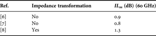
The purpose of this study is to investigate the attainable inductance ratios using the proposed topology while evaluating the impact it presents on the performance measures of the transformer. Thus, we extract the inductance values from the measured impedance parameters as in (2). In order to evaluate the overall performance of the component, we choose the minimum insertion loss (IL m) as a figure of merit, which considers simultaneously the quality factors Q P and Q S and coupling coefficient k of the transformer. Its value in decibels is extracted by (5) and (6), and is defined as the insertion loss of the two-port component in the best possible case, i.e., when both ports are perfectly matched. An overview of the attainable values for the minimum insertion loss found in the literature is presented in Table 1:
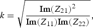
Table 1. Measured minimum insertion loss of integrated transformers at 60 GHz.
E) Different trace widths
1) CMOS MEASUREMENT
The first comparison we perform concerns the impact of presenting different trace widths for the primary and secondary. The structure of the considered CMOS transformers is shown in Fig. 4. They present the same secondary geometry consisting of a two-turn winding, with a 4-µm trace width, 1.5-µm spacing between turns, and a 42-µm average diameter. Primaries, on the other hand, present a 42-µm average diameter, so that they are centered above the secondaries. In the first case, as for a traditional design, the trace width is the same as for the secondary, i.e., 4 µm, and in the second case the primary is 12-µm wide, which corresponds to the maximum allowed width for this technology.

Fig. 4. 3-D view of CMOS transformers with (a) W P = 4 µm, and (b) W P = 12 µm.
The measurement results of these transformers are depicted in Fig. 5. It is observed that the proposed topology allows an increase from 3.1 to 4.2 on the inductance ratio at 60 GHz, as predicted by model simulation. On the other hand, the resonant frequency of the component is reduced, due to the augmentation of its effective capacitance. Nevertheless, mostly as a result of the stronger magnetic coupling, a better minimum insertion loss is achieved. Indeed, using the proposed topology, the minimum insertion loss is reduced from 1.3 to 1 dB at 60 GHz. Thus, we observe that the use of a wider primary above the secondary not only allows a higher transformation ratio, but also a better performance at mm-waves.

Fig. 5. (a) Primary quality factor and coupling coefficient, (b) minimum insertion loss, and (c) inductance ratio of CMOS transformers for different primary widths.
2) BiCMOS MEASUREMENT
In order to further evaluate this topology, we have designed three other transformers in the SiGe technology. This technology allows metal widths up to 30 µm, whereas the maximum allowed by the CMOS process is 12 µm. The secondaries of these transformers present two turns, with a 45-µm diameter, 4-µm trace width, and a 2-µm interturn spacing. Their primary diameter is equal to 45 µm, while the metal widths are, respectively, 12, 18, and 24 µm (Fig. 6).

Fig. 6. Layout of BiCMOS transformers with (a) W P = 12 µm, (b) W P = 18 µm, and (c) W P = 24 µm.
The obtained results (Fig. 7) confirm how transformation ratios are increased as primaries are wider. Hence, the obtained ratios at 60 GHz are as high as 4.8, 5.5, and 6.1 for respective primary widths of 12, 18, and 24 µm. In these cases, the resonant frequency is not strongly affected. Unlike the previous observation for CMOS transformers, widening the primary traces leads to a weaker magnetic coupling. This is due to the fact that the mutual inductance between the coils depends directly on the overlapping area between primary and secondary, which in this observation becomes proportionally lower as primaries are enlarged. The performance of the 12- and 18-µm transformers is very similar in terms of coupling and quality factor, and as a consequence, minimum insertion losses are equivalent for 12- and 18-µm primaries (IL m about 0.8 dB), and higher for the 24-µm transformer (1.2 dB). These results show that there is a limit on improving the performance of the transformers as transformation ratios are increased using the trace widths of the windings.

Fig. 7. (a) Primary quality factor and coupling coefficient, (b) minimum insertion loss, and (c) inductance ratio of BiCMOS transformers for different primary widths.
F) Different diameters
1) BiCMOS MEASUREMENT
We have also investigated the impact of designing transformers with different average diameters on the primary and secondary. Their layouts are presented in Fig. 8. We have taken advantage of the greater widths allowed for this process, so that the primary traces of the designed transformers are 18-µm wide. The primary diameter D P is 45 µm, secondary trace width is 4 µm, and secondary inter-turn spacing is 2 µm. The first transformer presents both primary and secondary with the same inner diameter (D S = 37 µm), for the second one the secondary is perfectly centered under the primary (D S = 45 µm), and for the third one outer diameters coincide (D S = 53 µm).

Fig. 8. Layout of BiCMOS transformers with (a) D S = 37 µm (D Sin = D Pin), (b) D S = 45 µm (D S = D P), and (c) D S = 53 µm (D Sout = D Pout).
Measured results are shown in Fig. 9. As expected, it is observed that greater diameters provide higher secondary inductances and hence higher transformation ratios. At 60 GHz, the inductance ratio is equal to 4 for the coincident inner diameters, 5.5 for the average diameters, and 7 for outer diameters. As it is observed that geometries presenting better coupling provide lower quality factors, we notice an equivalent minimum insertion loss in the three cases (IL m around 0.8 dB), when sufficiently distant from their resonant frequencies. It is moreover observed that resonant frequencies are lower for greater secondary diameters due to the increased equivalent capacitance to the substrate.

Fig. 9. (a) Secondary quality factor and coupling coefficient, (b) minimum insertion loss, and (c) inductance ratio of BiCMOS transformers for different secondary diameters.
These results prove that, for the metal width range allowed for this BiCMOS technology, it is possible to achieve a substantial increment on the inductance ratio by defining the relative diameter of the secondary under the primary without impacting on its losses.
IV. CONCLUSION
A novel layout topology to design transformers with high transformation ratios and compatible with mm-wave constraints was presented. This topology consists of defining different trace widths and different diameters for the stacked primaries and secondaries of the transformers. Experimental results of STMicroelectronics 65-nm CMOS and 130-nm SiGe BiCMOS components have been presented in order to support this study. The proposed electric model was shown to supply an accurate representation of the transformers' inductances. The obtained results proved the proposed transformers effective at providing higher inductance ratios than traditional topologies while reducing insertion losses, which are as low as state-of-the-art 1:1 transformers. Indeed, inductance transformation ratios as high as 7 at 60 GHz have been reported in our investigation. Such designs are simple to implement and constitute an interesting alternative to take advantage of the transformer properties to integrate matching networks within wireless communication-integrated circuits. Future developments could include investigating the impact of metal slotting in order to extend the achievable width ranges as well as differential characterization of the transformers.
 Bernardo Leite was born in Curitiba, Brazil, in 1984. He received his master's degree in electronics from ENSEIRB, University of Bordeaux, France in 2007, and is currently pursuing the Ph.D. degree in electronics at the IMS Laboratory, University of Bordeaux, France. His research interests include the design and modeling of on-chip passive components, and RF and mm-wave-integrated circuits.
 Eric Kerhervé received the Ph.D. degree in electrical engineering from University of Bordeaux, France in 1994. He joined ENSEIRB and the IMS Laboratory in 1996, where he is currently a professor in microelectronics and microwave applications. His main areas of research are the design of RF, microwave, and millimeter-wave circuits (power amplifiers and filters) in silicon and BAW technologies. He is and was involved in several European projects (Medea + UPPERMOST, Medea + QSTREAM, Catrene PANAMA, and FP6 MOBILIS), to develop silicon RF and mmW power amplifiers and BAW duplexer. He has authored and co-authored more than 190 technical papers in this field, and was awarded 17 patents. He has organized five workshops on advanced silicon technologies for radiofrequency and millimeter-wave applications. He is involved in the technical program committees of various international conferences (ICECS, IMOC, NEWCAS, EuMIC, SBCCI, LASCAS) and he was the chair of the international IEEE ICECS 2006 conference. He is co-editor of Special Issues for IEEE-ICECS'2006, IEEE-ICECS'2007, IEEE-LASCAS 2010. He is associate editor for IEEE Transactions on Circuits and Systems II (TCAS II). He is a member of the IEEE-CAS, IEEE-MTT, and IEEE SSCS.
 Jean-Baptiste Bégueret received the M.S. degree in electronics in 1990 and the Ph.D. degree in 1996, both from the University of Bordeaux, France. In 1997, he joined IXL, the microelectronics laboratory of University of Bordeaux, France, as an assistant professor, became associate professor in 1999 with the IC Design Team, where he leads the “High-Speed Mixed IC” Team since 2000. From 2005 to 2010, he was leading this “IC Design Team”. In 2006, he became a full professor in this University, in the IMS Laboratory (Laboratory of Integration, from Materials to Systems of the University of Bordeaux). From 2011, he is the head of the “Design Group”. His research interests are in silicon (SiGe, CMOS bulk, and SOI) ICs design for RF (up to 170 GHz) and high-speed data link (up to 100 Gbps) applications. He has been a member of the Technical Program Committee (TPC) of the IEEE Custom Integrated Circuit Conference (CICC). In 2002, he received the Best Paper Award at the “IEEE Asian Pacific Microwave Conference” in Japan. He is currently a member of the IEEE Bipolar/BiCMOS Circuits and Technology Meeting (BCTM) and the IEEE International Conference on Electronics, Circuits and Systems (ICECS) Steering Committee. He is also a member of the IEEE European Solid-State Circuits Conference (ESSCIRC), IEEE International Workshop on Radio-Frequency Integration Technology (RFIT), and the IEEE Radio Frequency Integrated Circuits Symposium (RFIC) Technical Program Committee. He is co-author of more than 150 publications in international conferences, journals, and 20 patents. In 2006, he was Technical Program Chair of the IEEE ICECS conference held in Nice, and in 2007, General Chair of IEEE PRIME conference in Bordeaux. In 2009, he received as a co-author the Best Paper Awards at the “IEEE NEWCAS-TAISA” and at “IEEE Symposium on Integrated Circuits and Systems Design (SBCCI)”.
 Didier Belot received the “D.U.T Electronique” degree from the “Institute Universitaire de Technologie” of Grenoble, Grenoble France in 1982, and the M.S degree from the “Ecole Nationale Superieure d'Electronique et de Radioelectricite de Grenoble”, Grenoble France in 1991. In 1983, he joined the Bipolar Device Characterization and Modelization group, Thomson Semiconductor. In 1986, he joined Thomson “Etude et Fabrication de Circuits Integres Speciaux”, where he was involved with digital CMOS design. In 1988, he was involved with the design of high speed ECL/CML data communication ICs at STMicroelectronics. In 1996 he moves to the Radio Frequency design. From 1999 to 2005 he managed an RF-Analog design group which has developed WPAN and 3 G transceivers in BiCMOS and CMOS processes. At present, he manages the Minatec Advanced R&D Analog RF team which develops new solutions for early RF and mmW standards for STMicroelectronics, Crolles & Minatec Grenoble, France.


