Introduction
Since the 1990s, pulsed power technology has continued to progress in the direction of ultra-high power and high-energy of single-pulse systems to meet the needs of flash radiography, X-ray generation, inertial confinement fusion, and so on (Quintenz, Reference Quintenz2004; Deng et al., Reference Deng, Shi, Xie, Zhang, Feng, Li, Wang, Xia, Dai, Li, Li, Wen, Chen, Li, Huang, Lai, Zhang, Xia, Guan, Song, Chen, Ji, Zhou, He, Zou, Huang, Zhou, Zhang, Zhang, Ren, Wei, Tian, Yang, Li, Xie, Liu, Ma, Ma, Wang, Wang, Yang, Gu, He, Li, Zhou, Zhang, Dai, Wang, Chen, Liu, Sun, Xu, Meng and Ma2015, Reference Deng, Xie, Feng, Wang, Li, Song, Xia, Ji, He, Tian, Gu, Guan, Wei, Huang, Ren, Dan, Li, Zhou, Cai, Zhang, Wang, Xu, Wang, Zhang, Wang, Guo, He, Zhou, Zhang, Yang and Zou2016; Ding et al., Reference Ding, Zhang, Xiao, Wu, Dai, Yin, Gao, Sun, Xue, Ning, Shu and Wang2016). At the same time, driven by the demand for directed energy applications such as high-power microwaves, the development of compact repetitive pulsed power technology is accelerating (Gaudet et al., Reference Gaudet, Barker, Buchenauer, Christodoulou, Dickens, Gundersen, Joshi, Krompholz, Kolb, Kuthi, Laroussi, Neuber, Nunnally, Schamiloglu, Schoenbach, Tyo and Vidmar2004; Kim et al., Reference Kim, Kovalchuk, Kokshenev, Shishlov, Ratakhin, Oreshkin, Rostov, Koshelev and Losev2016). Initially, miniaturization of high-power microwave systems was focused on high-power microwave devices. As the mobility requirements of high-power microwave systems have increased, research has begun to pay more and more attention to the miniaturization of pulsed power sources (Korovin et al., Reference Korovin, Rostov, Polevin, Pegel, Schamiloglu, Fuks and Barker2004; Pan et al., Reference Pan, Yang and Cheng2016; Zhang et al., Reference Zhang, Ge, Zhang, He, Fan, Li, Jin, Gao, Ling and Qi2016). The Multidisciplinary University Research Initiative (MURI) program on compact, portable, pulsed power that began in the USA in 2001 (Gaudet et al., Reference Gaudet, Barker, Buchenauer, Christodoulou, Dickens, Gundersen, Joshi, Krompholz, Kolb, Kuthi, Laroussi, Neuber, Nunnally, Schamiloglu, Schoenbach, Tyo and Vidmar2004) was mainly focused on the fundamental research on the essential components of compact pulsed power for directed energy application. A series of compact pulsed power generators based on Tesla transformers and their applications has been developed and researched in Russia (Mesyats et al., Reference Mesyats, Korovin, Gunin, Gubanov, Stepchenko, Grishin, Landl and Alekseenko2003, Reference Mesyats, Korovin, Rostov, Shpak and Yalandin2004; Kim et al., Reference Kim, Kovalchuk, Kokshenev, Shishlov, Ratakhin, Oreshkin, Rostov, Koshelev and Losev2016). Compact repetitive pulsed power research began at IAE in the early 2000s with the development of helical high-current accelerator (650 kV, 6.5 kA, 210 ns, 20 Hz) (Cao et al., Reference Cao, Tan, Fan, Hu, Wu and Hou2006). IAE developed a further type of pulse accelerator (1 MV, 20 kA, 40 ns, 100 Hz) based on Tesla transformer in 2006 (Zhang et al., Reference Zhang, Chang, Xiang, Song, Kang, Luo, Li and Gong2007), followed by a repetitive pulse generator (800 kV, 8.5 GW, 180 ns, 25 Hz) based on a Linear Transformer Driver (LTD) in 2010 (Xiang et al., Reference Xiang, Tan, Zhang, Wang, Luo, Cao, Kang, Gong, Luo, Li, Jin and Zhang2010). Though the three pulsed power systems mentioned above have a good performance and repeatability, their sizes and weights are still too large. Since 2010, IAE has embarked on more compact pulsed power system research. In order to minimize the size and weight, a simplified bipolar charged Marx circuit was proposed with a series of pulsed power generators developed based on the simplified Marx circuit. The detailed simplification of the Marx circuit is described in section “Simplification of Marx circuit”. Research and developments on several key technologies and components, such as compact pulse-forming modules, a compact and repetitively triggered spark-gap switch, a high-voltage bipolar charging power supply with high precision and high average power, and a fast rise-time trigger source with low jitter and high energy are presented in section “Continuing research and development of key technologies and vital components”. Several typical compact repetitive Marx generators are described in section “Development of repetitive pulsed power generators”.
Simplification of Marx circuit
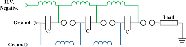
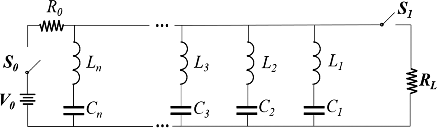
The Marx circuit widely used in the high-power pulsed generators is a voltage-multiplying circuit that charges a number of capacitors in parallel and discharges them in series (Lehr and Ron, Reference Lehr and Ron2017). Figure 1 shows a typical single-sided charged Marx generator, where a number N of switches and of capacitors are used, producing an open-circuit voltage of NV 0 (where V 0 is the charging voltage). A bipolar charged Marx circuit is shown in Figure 2, where N switches and 2N capacitors are used, producing an open-circuit voltage of 2NV 0. The advantage of this bipolar charged Marx circuit is that it has half the number of switches but twice the stage voltage for a given output voltage. An isolation resistor to ground is connected between the two capacitors of each stage in the conventional bipolar charged Marx generator, as shown in Figure 2. The isolation resistor chain may be replaced by an inductor chain to enable faster charging and to attain the capability of repetitive operation, and reduce the time of electric stress on the insulation during charging.

Fig. 1. A typical single-sided charged Marx generator.

Fig. 2. A typical bipolar charged Marx generator.
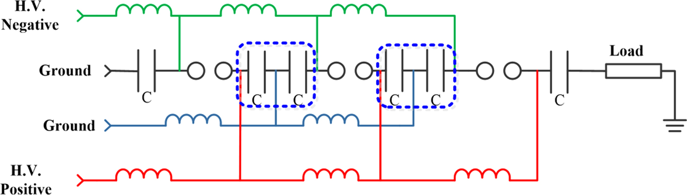
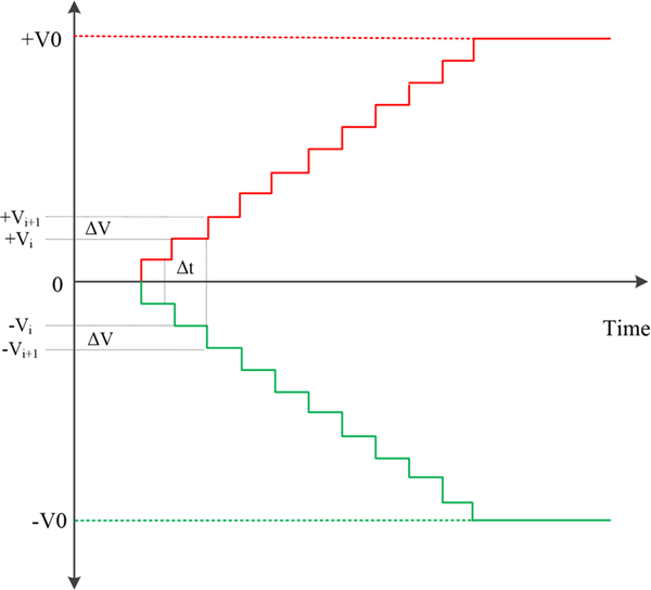
Without affecting the basic characteristics of the Marx circuit, removal of the grounding resistors from the Marx circuit and the combination of two capacitors of the same stage into one capacitor will further simplify the circuit, as shown in Figure 3. The capacitance of the first and last capacitors are both C 0, and the capacitance of 2nd to (N–1)th are C 0/2. If the capacitors are replaced by pulse-forming lines (PFL) or pulse-forming networks (PFN), an output pulse with flat-top duration can be obtained, as shown in Figure 4, where the waveform obtained using the simplified Marx circuit is the same as that of the conventional bipolar charged Marx circuit. This simplified Marx circuit reduces the number of capacitors and eliminates the resistors to ground, which facilitates miniaturization of the pulsed power system.

Fig. 3. Simplified bipolar charged Marx generator.
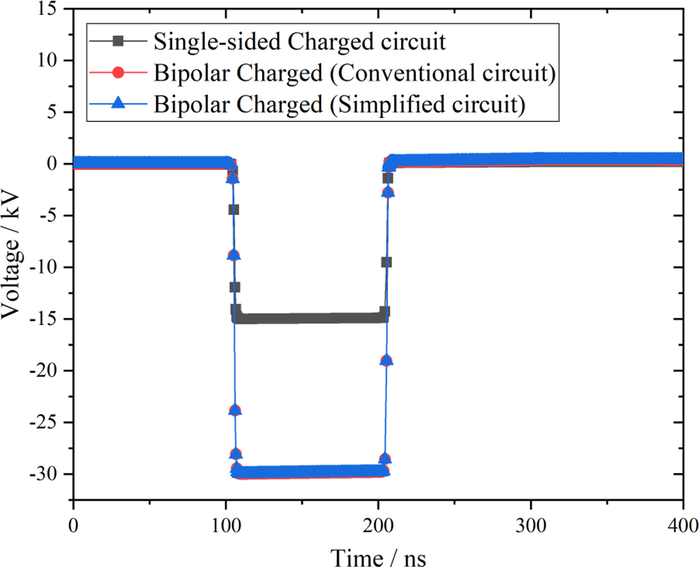
Fig. 4. Comparison of the output waveforms using three types of Marx circuits based on PFL.
Continuing research and development of key technologies and vital components
Pulse-forming modules
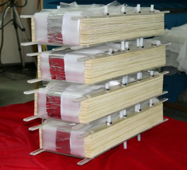
Several different kinds of pulsed forming modules were developed at IAE, such as thin-film dielectric PFLs, PFL based on Printed Circuit Board (PCB), and non-uniform PFN. Thin-film dielectric PFL is easy to fold and wind (Smith et al., Reference Smith, Champney, Hatch, Nielsen and Shope1971; Schamiloglu et al., Reference Schamiloglu, Schoenbach and Vidmar2003; Ouyang et al., Reference Ouyang, Liu, Liu, Wang and Feng2008), which is beneficial to the miniaturization of pulse power sources. Figure 5 shows a compact, portable, layer-wound mylar dielectric Blumlein line, having the dimensions of 50 cm × 18 cm × 12 cm, maximum withstand voltage of 60 kV, and a pulse width of 180 ns (Gan et al., Reference Gan, Song, Zhuo, Qin, Zhang, Gong and Jin2012). Figure 6 shows the typical output waveform of a layer-wound Blumlein line. As can be seen that there is a pre-pulse about 90 ns before the voltage waveform due to the spatial electric field coupling to the load. Affected by the coupling effect, the pulse amplitude decreases during the second half of the main pulse.
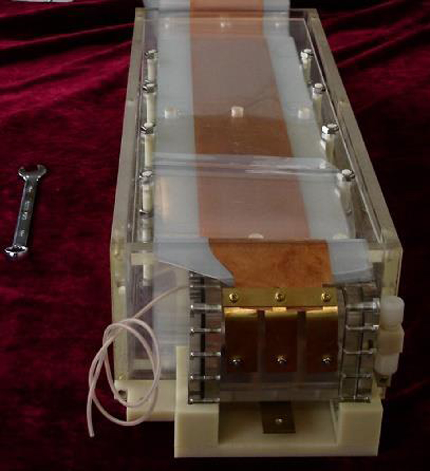
Fig. 5. Compact, portable layer-wound Blumlein line.
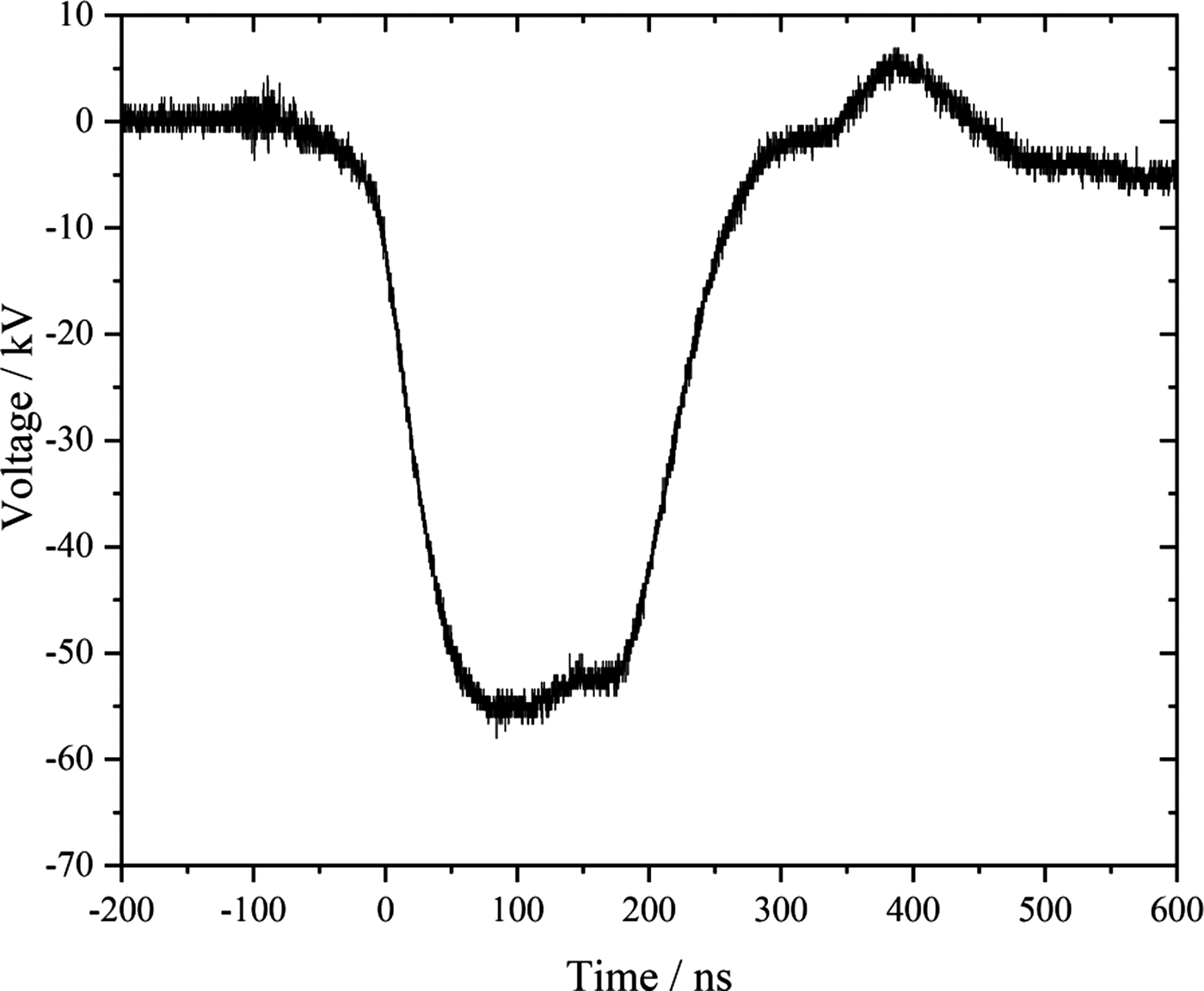
Fig. 6. Output waveform of layer-wound Blumlein line.
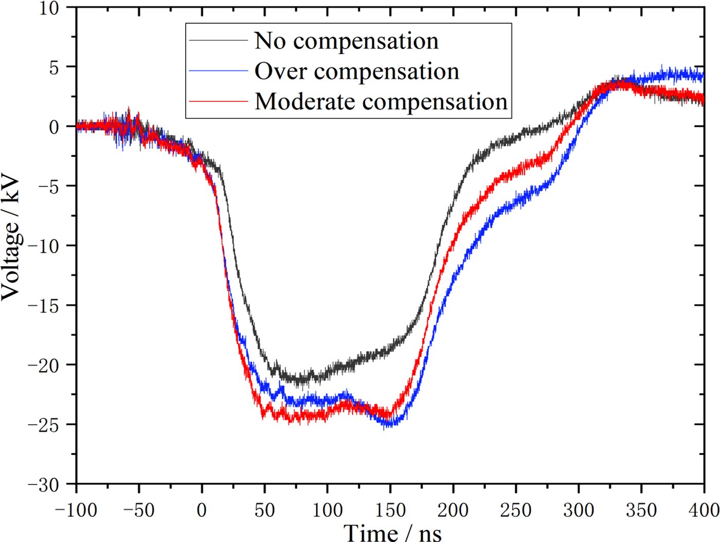
In order to reduce the influence of the coupling effect on the flat-top of the pulse waveform, the characteristic impedance of the second half of the Blumlein line is changed to a gradient impedance to compensate the output waveform. Figure 7 shows the thin plate-isolated Blumlein lines. The output waveforms before and after impedance compensation were shown in Figure 8. The results show that a waveform with a better flat-top is obtained after the compensation.
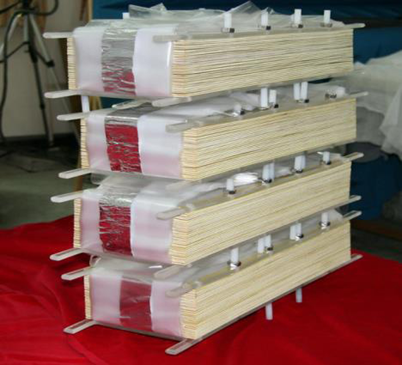
Fig. 7. The thin plate-isolated Blumlein lines.

Fig. 8. Output waveforms of the thin plate-isolated Blumlein line with and without impedance compensation.
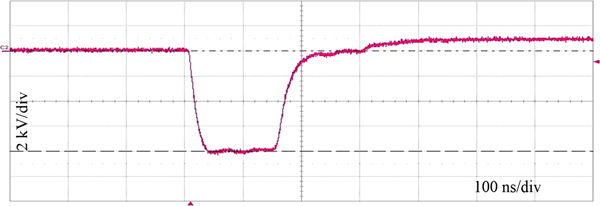
A spiral strip Blumlein line with a withstand voltage of 100 kV and a pulse width of ~200 ns was developed (Song et al., Reference Song, Qin, Zhuo, Gan, Luo, Gong and Jin2012). This type of line is spirally wounded on a flat insulator of Polymethyl methacrylate, as shown in Figure 9. This type of PFL has a relatively wide pitch and layer spacing, so the output waveform is not affected by the coupling effect, and the spiral winding makes the structure more compact. The thickness of the thin-film dielectric layer is determined by the designed characteristic impedance and withstand voltage. An output waveform with a rise time of 40 ns, a pulse width of 207 ns, and a flat-top of 140 ns is obtained, as is clear from Figure 10.

Fig. 9. Schematic of a layer-wound spiral strip line.
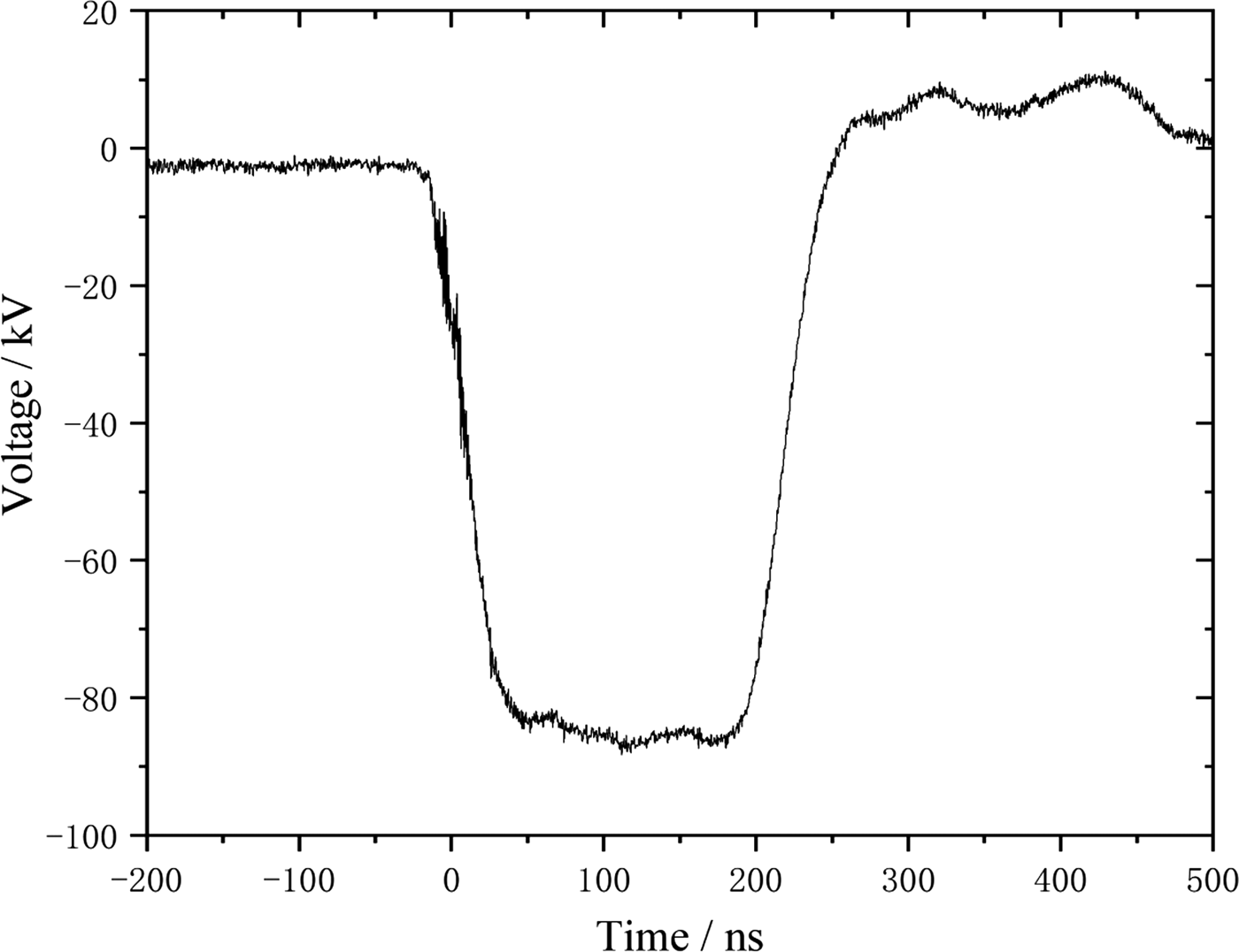
Fig. 10. Output waveform of spiral strip line with charging voltage of 100 kV.
In order to meet the requirement of a relatively low-power pulsed system, a more compact solid-state PFL based on a PCB was developed (Li et al., Reference Li, Chang, Song, Qin, Gan, Gong and Jin2013). Figure 11a shows a planar S-type folded PFL with a withstand voltage of 50 kV. A multi-stage PFL module was designed in parallel in order to reduce the characteristic impedance and improve the energy-storage density, as shown in Figure 11b. A typical output waveform having a pulse width of 140 ns and a flat-top width of 100 ns is shown in Figure 12. This kind of PFL has a pulse square wave with good flat-top, but a low withstand voltage due to the limitation of the dielectric material of PCB. It is suitable for use in relatively low-power, low-voltage pulsed circuits.
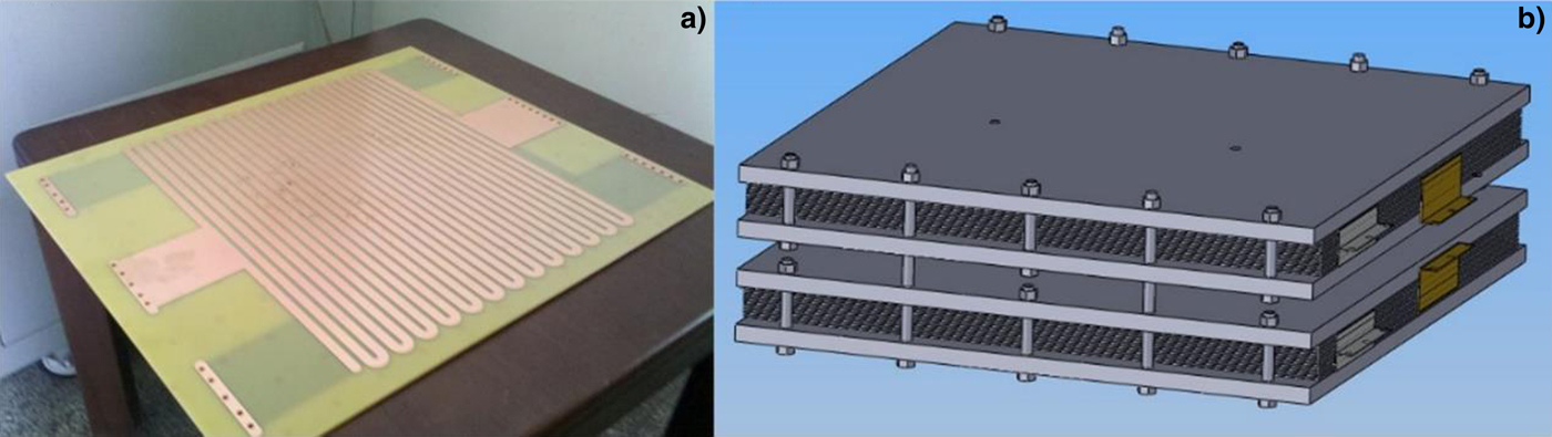
Fig. 11. S-type folded planar pulse-forming line based on PCB, (a) single module, (b) multi-stage parallel modules.

Fig. 12. Output waveform of S-type folded planar PFL.
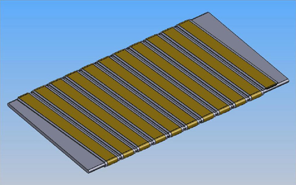
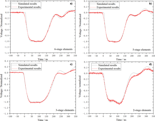
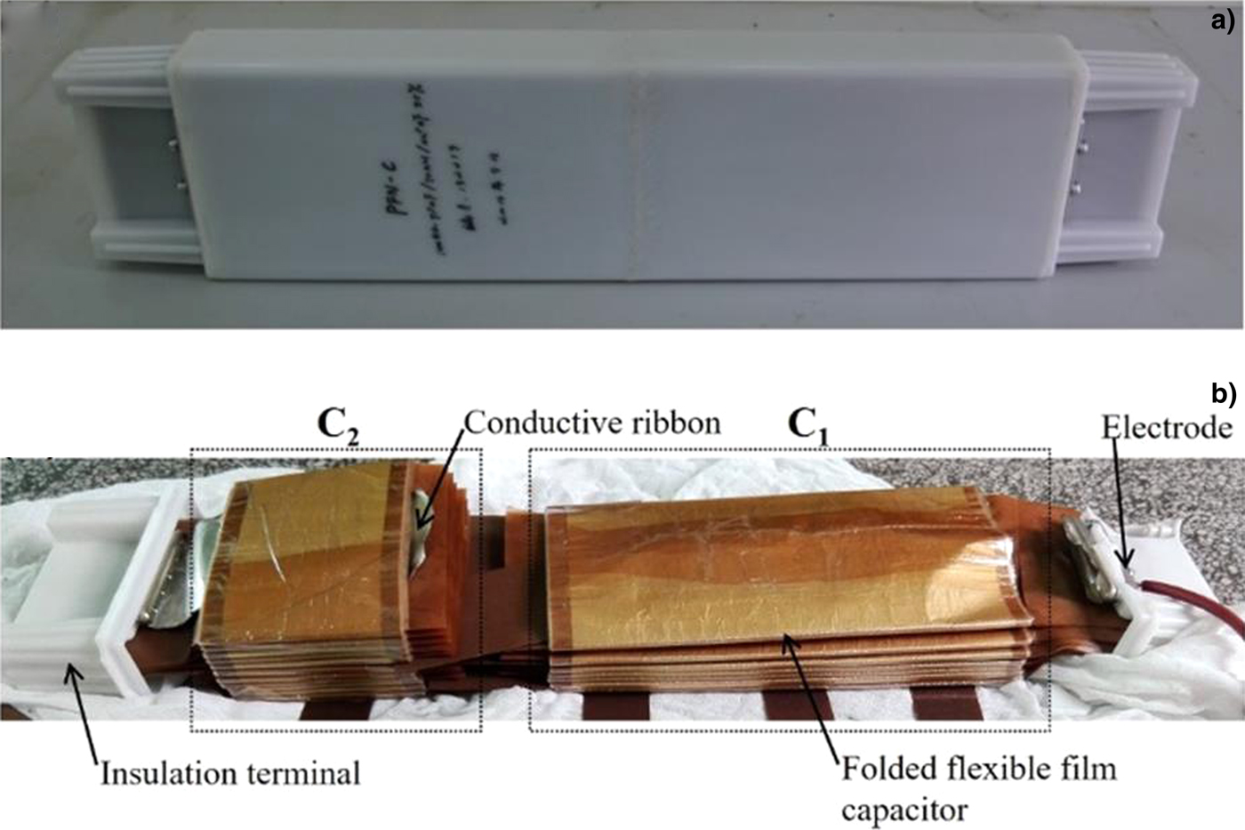
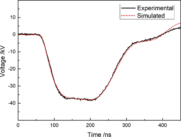
The PFN is a typical square wave pulse-forming technique using L-C circuit. Figure 13 shows an equivalent electrical circuit for the Guillemin type C network with n branches (Li et al., Reference Li, Song, Zhu, Jin, Gan and Gong2018). The experimental results show that when the L-C cell number of the Guillemin type C network is gradually reduced from 6 to 2, a good square-wave pulse can still be obtained, as shown in Figure 14. Therefore, in attempts to obtain a quasi-square waveform with flat-top under a compact structure, a low-inductance pulse-forming module based on two-cell L-C circuit was designed and fabricated (Li et al., Reference Li, Song, Zhu, Jin, Gan and Gong2018). The two-cell PFN was encapsulated in a shell and appears similar to a conventional capacitor, as shown in Figure 15. The dimensions of the two-cell pulse-forming module with an impedance of 2.5 Ω are 720 mm × 155 mm × 62 mm, and its energy storage density can reach 42 kJ m−3. The research results show that the developed pulse-forming module has a withstand voltage of 120 kV, a pulse of 180 ns, and a flat-top of 100 ns. Simulated and experimental output waveforms are given in Figure 16.

Fig. 13. Equivalent circuit for Guillemin type C network with n branches.
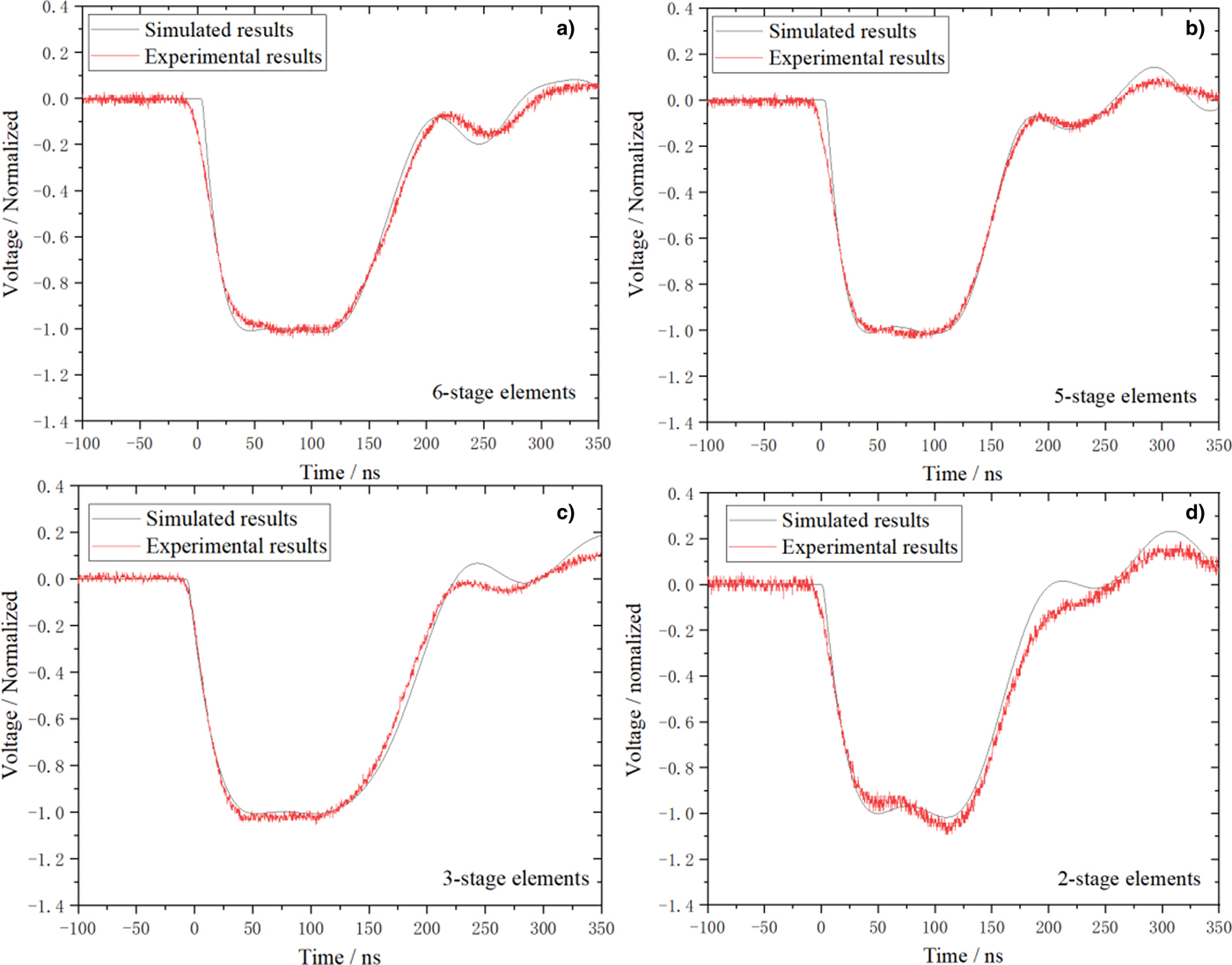
Fig. 14. Experimental and simulated results of different branches of Guillemin network.

Fig. 15. Picture of the pulse-forming module and internal structures.
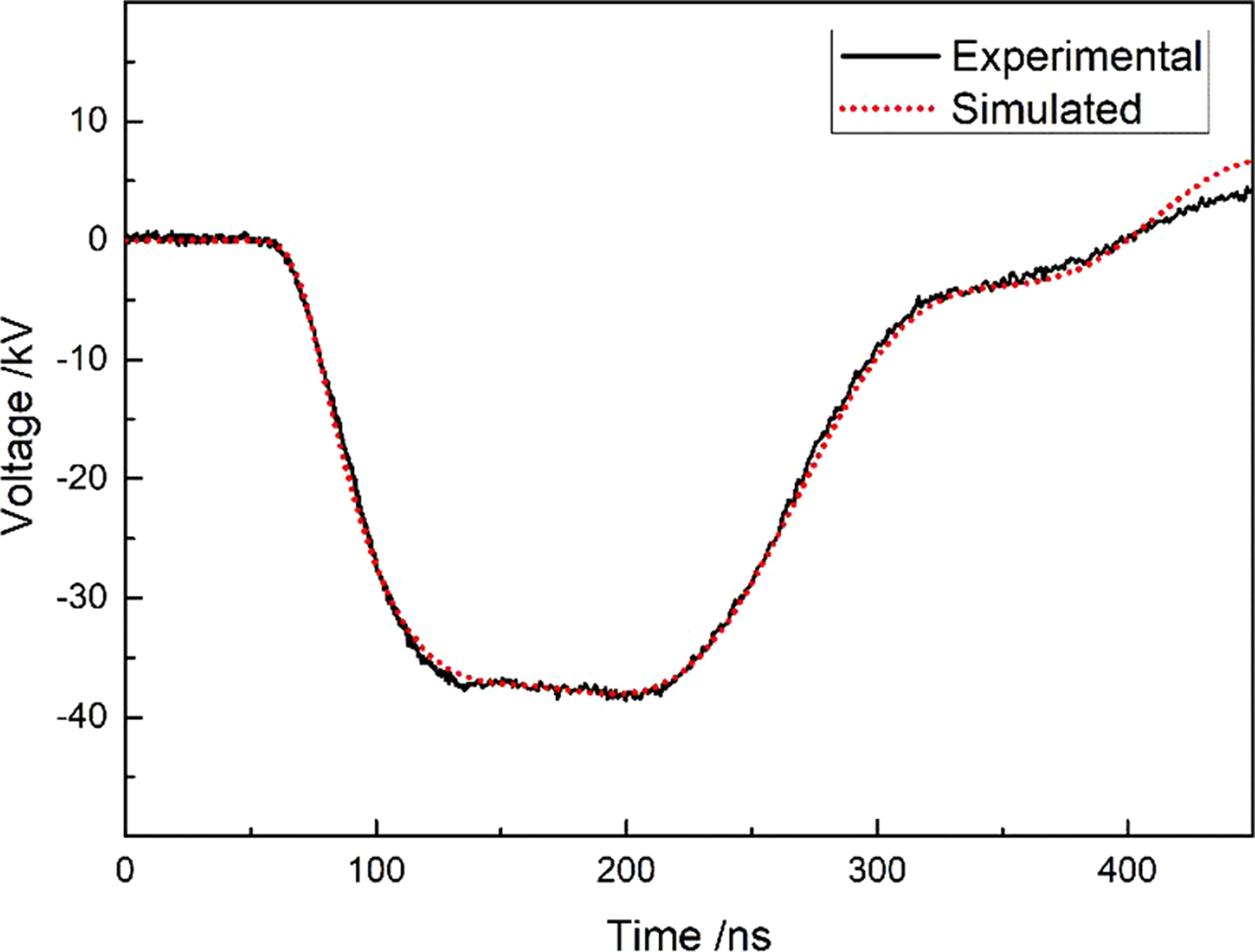
Fig. 16. Simulated and experimental output waveforms.
Three-electrode spark-gap switch with low jitter and high current
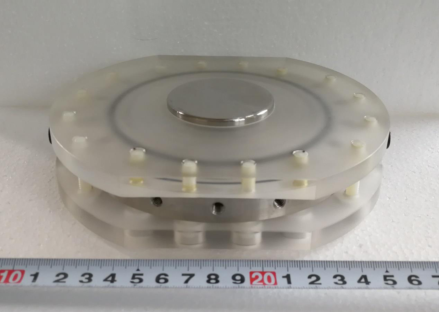
The spark-gap switch is a key component of an only pulsed power source with the performance of the switch directly influencing the output characteristics of the overall pulsed power system. Based on the application requirements of the repetitive pulsed power source, a small field distortion three-electrode spark gap switch was designed, developed, and studied (Zhang et al., Reference Zhang, Song, Zhang, Zhang, Gan, Gong and Jin2018), as shown in Figure 17. The compact switch has a small size of only 150 mm × 42 mm, a light weight of about 1.5 kg, and a high withstand voltage of over 112 kV. The switch filled with a mixed gas of 30% SF6 and 70% N2 has a wide voltage operating range of 31–90, 42–85% of the pulsed self-breakdown voltage at the gas pressures of 0.1, 0.4 MPa, as shown in Figure 18. It can be operated stably at a repetition rate between 1 and 50 Hz with a jitter of <4 ns, as shown in Figure 19. Its service life has exceeded 100 000 shots under the on-current of 8.5 kA.

Fig. 17. Photo of the small field distortion spark-gap switch.
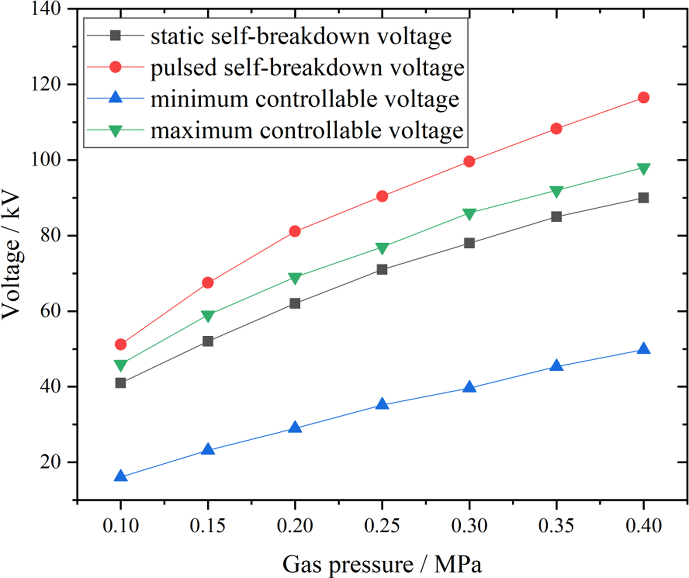
Fig. 18. Operating voltage range of the switch versus gas pressure.
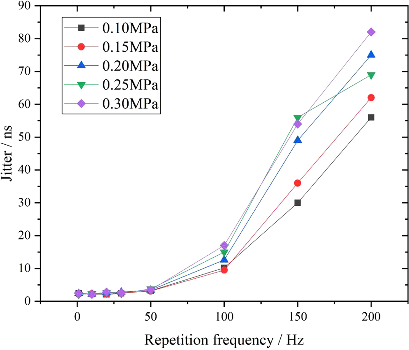
Fig. 19. Variation of jitter with the repetition frequency.
High precision and high-power repetitive power supply
Since there are no resistors or inductors to ground in a simplified Marx circuit, the potential of the capacitors is suspended during charging, which causes the positive and negative voltages of a capacitor to be inconsistent or even impossible to be charged. A special constant current charging power system was therefore developed (Gan et al., Reference Gan, Song, Lei, Luo, Zhang, Wang, Gong and Jin2018), as shown in Figure 20. A real-time comparison circuit was used in the control mode. After each small step is completed, the control system compares the positive and negative voltages so as to confirm whether they are consistent. If there is a deviation, the part with larger voltage is hold constant with the other part adjusted until the two voltages are equal. Then the joint charges are continued and repeated iteratively in order to realize the positive and negative voltage synchronous charging. Figure 21 gives the real-time comparison charging schematic.
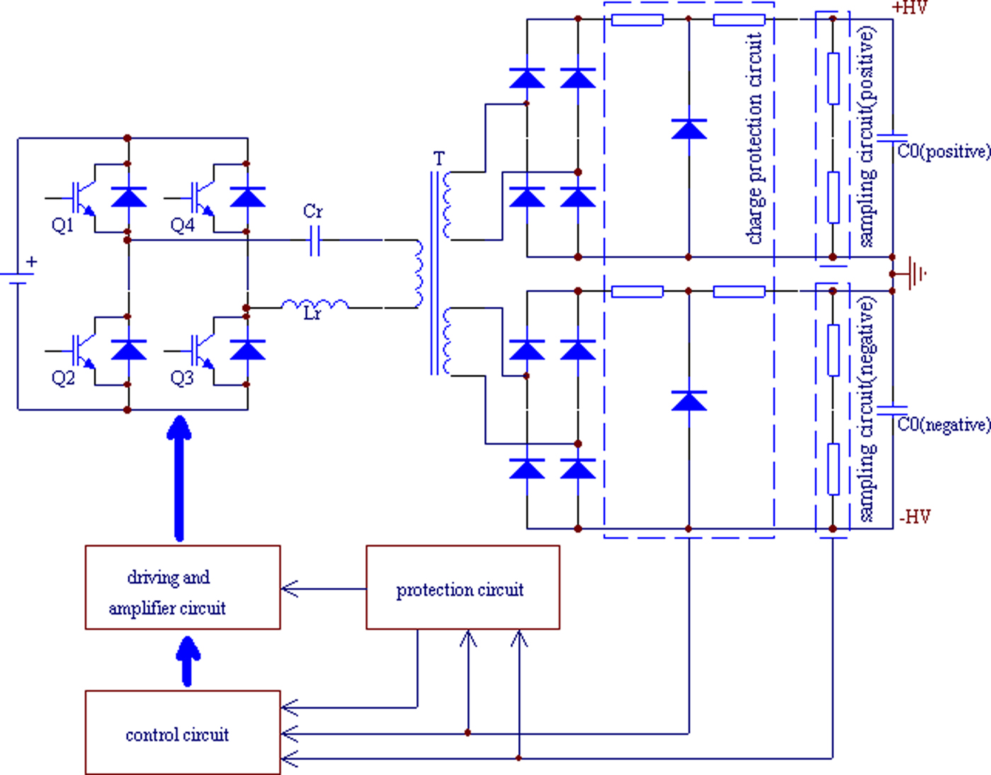
Fig. 20. Equivalent circuit of series resonant charger.

Fig. 21. A step comparison charging schematic.
Based on this design idea, a compact high-power pulse charging power supply was developed, with an output voltage between ±10 and ±50 kV, a charging accuracy of 0.1 kV, a charging current of 2.5 A, and a repetition frequency continuously adjustable between 1 and 50 Hz. The power supply has a small volume of 1.7 m × 1.5 m × 0.5 m, a light weight of 300 kg, with strong anti-interference abilities and a short-circuit capability. In practice, it has been applied to a repetitively high-power pulse power source.
Low-jitter high-energy trigger source
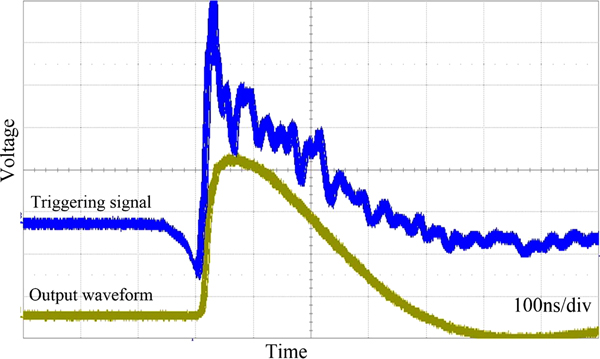
In order to reduce the delay time jitter of a repetitive pulse generator, a low-jitter and repetitively high-energy trigger source was developed (Li et al., Reference Li, Song, Gan, Jin and Zhu2017). The source consists of a ±50 kV charging power supply, a Hydrogen-thyristor pulse source with an output voltage of 80 kV, two 30 nF capacitors, a three-electrode spark gap switch, and a high-power solid resistor of 300 Ω, as shown in Figure 22. The output pulse has a rise time of 30 ns, a width of 200 ns, a maximum output voltage of 95 kV, and a maximum storage energy of 75 J. It can run with 30 pulses at a repetition rate of 30 Hz and a jitter of only 2 ns, as shown in Figure 23.
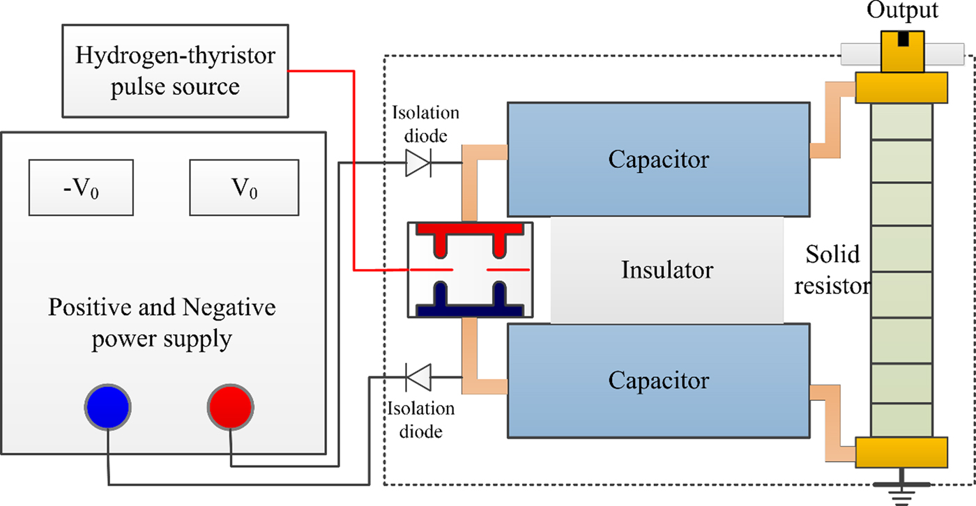
Fig. 22. Layout of the high-energy trigger source.

Fig. 23. Output waveforms of high-energy trigger source.
Development of repetitive pulsed power generators
Low-impedance Marx generator
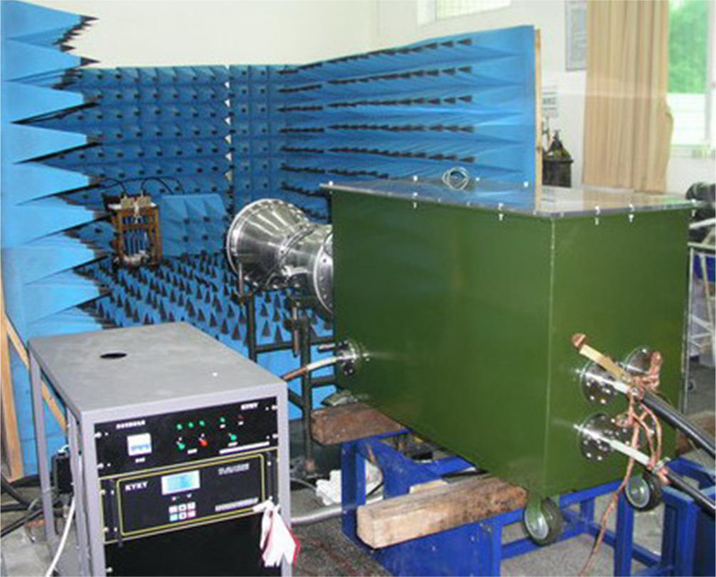
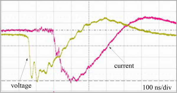
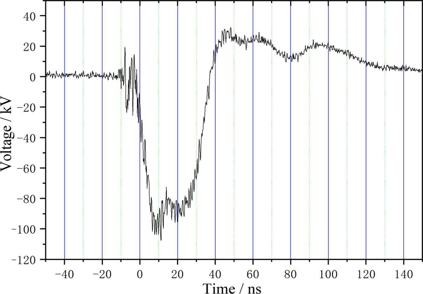
A low-impedance Marx generator with an output voltage of 628 kV, a current of 52 kA, a rise time of 97 ns, a storage energy of 5 kJ, and dimensions of 1.2 m × 0.5 m × 0.6 m was developed (Qin et al., Reference Qin, Song, Gan, Gong, Zhuo, Luo and Jin2012), as shown in Figure 24. Based on this generator, a low-impedance magnetically insulated line oscillator (MILO) was directly driven (Song et al., Reference Song, Gan, Zhang, Qin, Luo, Wang, Chen, Wen, Gong and Jin2013). With an electron-beam voltage of ~450 kV and a current of ~40 kA, the radiated microwave had a peak power of 400 MW, a pulse width of 60 ns, and the center frequency of 1.23 GHz. Figure 25 shows the voltage and current waveforms of the low-impedance Marx generator with a MILO as the load.

Fig. 24. Photo of a low-impedance Marx generator for high-power microwave application.
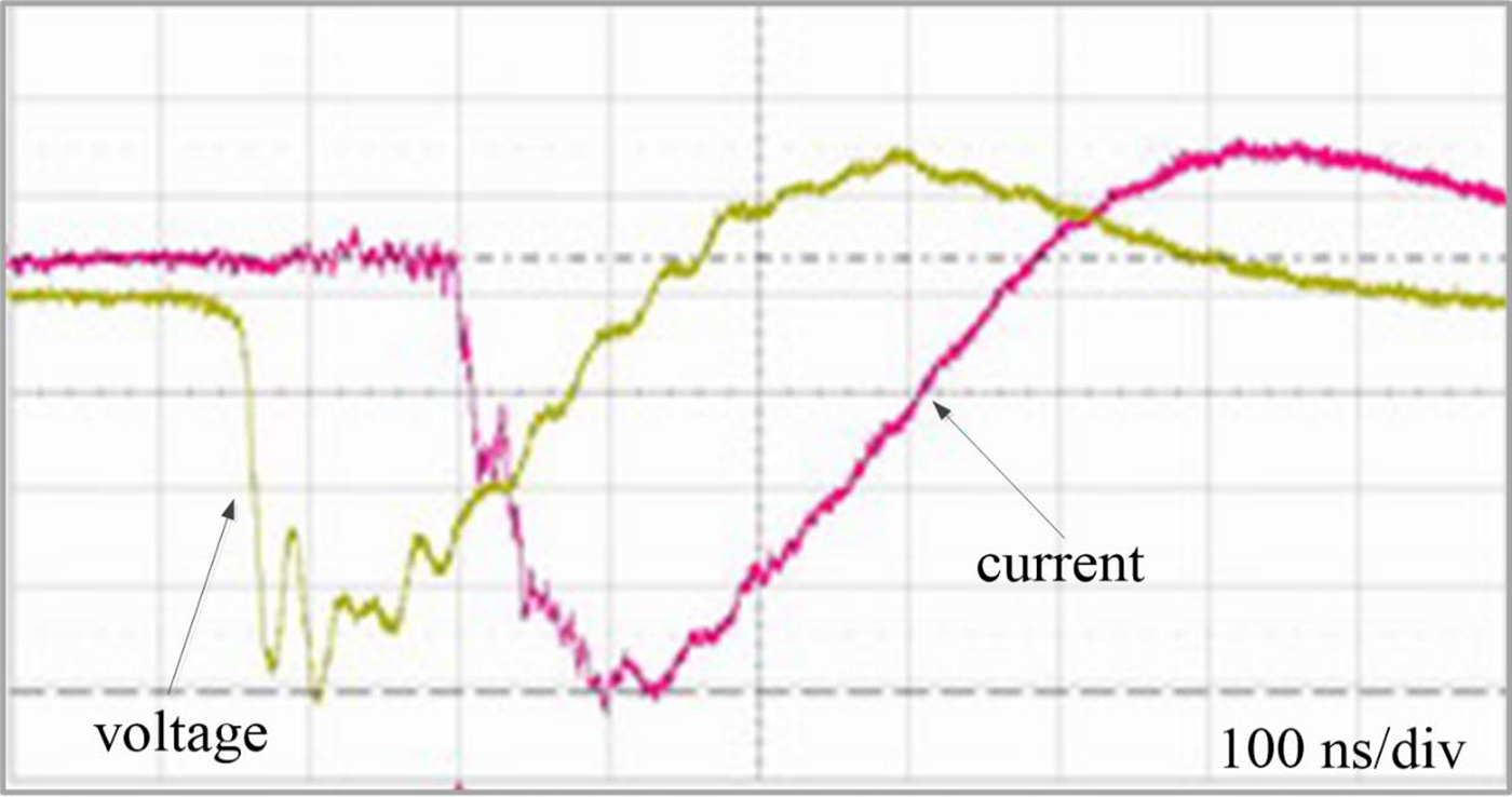
Fig. 25. Voltage and current waveforms of low-impedance Marx generator.
Square-wave pulse generator based on Kapton-film dielectric line
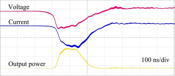
A square-wave pulse generator based on Kapton-film dielectric Blumlein line using the simplified Marx circuit was developed (Song et al., Reference Song, Li, Qing, Gan, Luo, Gong and Jin2017b), as shown in Figure 26. The output pulse obtained had a peak power of 4 GW, a width of 156 ns, a rise time of 40 ns when feeding on a 60 Ω water resistor load. It could be operated at a repetition rate of 10 Hz. Figure 27 shows the output waveform in both single shot and a repetition rate of 10 Hz.

Fig. 26. Photo of pulse generator based on Kapton-film dielectric line.
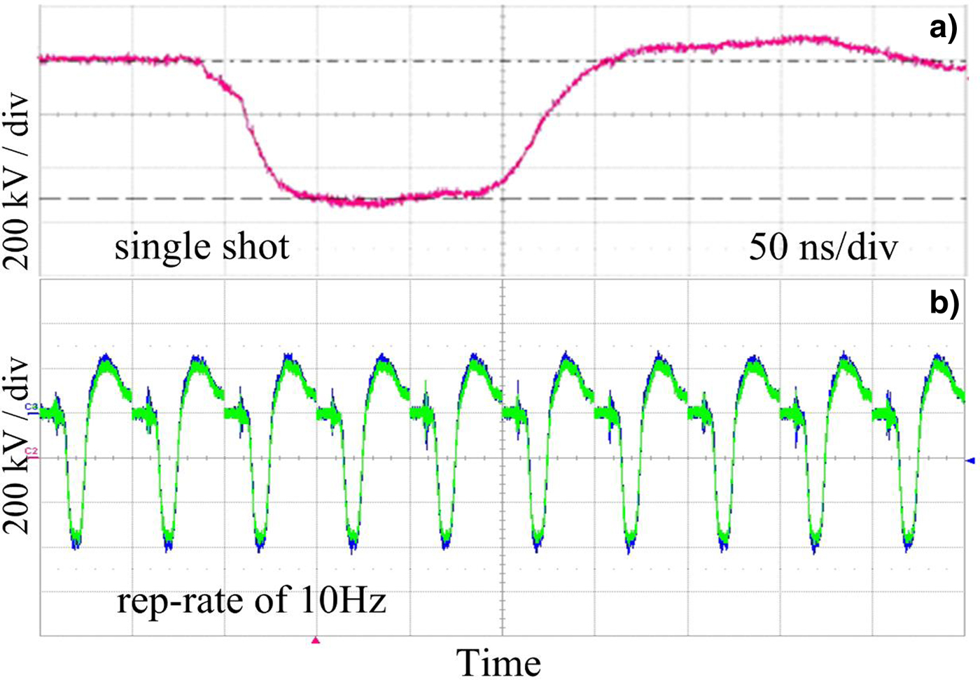
Fig. 27. Output waveforms of pulse generator based on Kapton-film dielectric line at (a) single shot and (b) repetition rate of 10 Hz.
High pulse-energy repetitive PFN-Marx generator
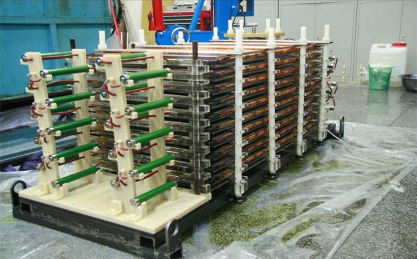
A compact and repetitively high pulse-energy PFN-Marx generator with low jitter was developed using the simplified bipolar Marx circuit (Song et al., Reference Song, Jin, Li, Luo, Zhang, Wang, Li, Su, Zhuo, Jin, Gan and Gong2017a, Reference Song, Li, Zhang, Gong, Gan and Jin2019), as shown in Figure 28. The size and weight of the generator were minimized by using two-cell pulse-forming modules as described earlier, alternating two superposition structures on both sides and high electric field shielding technology. The generator has a total volume of 2.5 m3 and a weight of 2.2 tons, making it much more compact than conventional pulsed power sources. Experimental results demonstrated that when the generator operates with a single pulse output, the voltage, current, and peak power are 0.98 MV, 19.6 kA, and 19.2 GW. The total energy storage in the Marx tank is about 3.9 kJ. When the generator was operated at a repetition rate of 30 Hz, the output pulse had a peak power of 16.7 GW obtained as shown in Figure 29. The voltage fluctuation range is limited to within ±1.5%, and the current fluctuation range is limited to within ±2%. The delay time jitter between the trigger pulse and the output pulse is <6.5 ns standard mean deviation. Statistical distributions of the delay time jitter and current amplitude variation of the 300 pulses are approximately Gaussian.

Fig. 28. Structural diagram of high pulse-energy repetitive PFN-Marx generator.

Fig. 29. The waveforms of 30 pulses on a plane diode.
Coaxial Marx generator based on ceramic capacitors
A compact coaxial Marx generator with a 3.3 nF ceramic capacitor as the stage storage capacitance was developed (Gan et al., Reference Gan, Song, Zhuo, Zhang, Qin, Gong and Jin2013). When operating at a repetition rate of 100 Hz, a pulse with a voltage of 150 kV, a width of 25 ns, and a rise time of 10 ns was obtained on a 50 Ω resistive load. The maximum voltage can reach 240 kV on open circuit. Figure 30 shows the generator, which is Ф200 mm × 550 mm in size, and Figure 31 shows a typical output waveform with an output voltage of 100 kV.
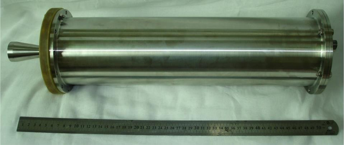
Fig. 30. The photo of coaxial Marx generator.

Fig. 31. A typical output waveform of coaxial Marx generator.
Conclusion
This paper reviews the progress of the miniaturization of repetitive pulsed power sources in recent years at IAE. A simplified bipolar Marx circuit was proposed and has been applied to the development of various types of compact pulsed power sources, laying a foundation for future miniaturization and practical application. The development of pulsed power technology is inseparable from market demands, and the miniaturized pulsed power system needs to undergo a transition from laboratory device to industrial equipment. The development of miniaturized pulsed power sources with a high average power-to-volume ratio, high reliability, and long lifetime is one of the main directions for the future. To realize the market-oriented application of high-energy pulsed power sources, further researches are needed in the following aspects: (1) primary high-energy density storage technology, (2) pulse shaping and waveform control technology in compact structures, (3) high current switch with low jitter and long lifetime, (4) system thermal management technology.
Author ORCIDs
Falun Song, 0000-0002-9666-6813.