Introduction
The 3-dB branch-line couplers are essential components in wireless communication systems. They are used for splitting/combining microwave signals. Classical branch-line couplers, which are based on four quarter-wavelength (λ/4) transmission lines, suffer from their large size, especially for low frequencies. Several miniaturization techniques in planar technologies have been proposed to reduce the physical dimensions of the (λ/4) transmission lines. The use of fractal space-filling allows size miniaturization of a rat-race hybrid up to 40%, however, λ/4 transformers were needed in order to have an acceptable matching level in the operating bandwidth [Reference Ghali and Moselhy1, Reference Caillet, Clenet, Sharaiha and Antar2]. In [Reference Jung, Negra and Ghannouchi3], high impedance transmission lines with distributed capacitors inside the open coupler area resulted in 38% miniaturization at the expense of circuit complexity. Besides, the use of discontinuous microstrip lines can offer a size reduction up to 60% at the expense of circuit complexity [Reference Sun, HO, Yen and Weide4]. All the above techniques involve the knowledge of new topologies and huge design efforts from design engineers.
In this paper, the effort is carried out on substrate technology. Hence classical shape of the coupler is proposed, thus simplifying the engineer's design task, while achieving a high degree of miniaturization, as compared with classical microstrip lines couplers, along with high electrical performance.
The proposed compact branch-line coupler is based on the slow-wave concept using a double layer printed circuit board (PCB) substrate. The slow-wave effect is achieved thanks to the insertion of blind metallic via holes in the lower substrate layer, leading to slow-wave microstrip lines (SMS lines). From a circuit point of view, the presence of these blind via holes increases the transmission line equivalent capacitance per unit length, thus reducing the wave propagation velocity and creating consequently the slow-wave effect. A similar concept of slow-wave effect was previously proposed in [Reference Niembro, Nassereddine, Pistono, Issa, Franc, Vuong and Ferrari5] and successfully applied on substrate integrated waveguides, allowing a size reduction of 60% as compared with classical SIW. In [Reference Coulombe, Nguyen and Caloz6], “Substrate Integrated Artificial Dielectric” structure was presented to reduce the size of microstrip circuits by using a mesh of blind via holes connected to the ground plane. A size reduction of 33% was obtained for a 2 GHz branch-line coupler with 4-dB insertion loss at the working frequency. Drawbacks of this structure are the huge number of required via holes, leading to high insertion loss, and the design complexity since the relative position of vias underneath signal strips depends on the vias matrix dimension. Furthermore, using a high number of via holes does not lead necessarily to better slow-wave effect since the vias that are far from the strip do not contribute to the slow wave concept as it will be explained later. In this paper, the design of the miniaturized coupler is greatly simplified by only considering one row of the blind via holes underneath the signal strip. Moreover, thanks to the limited number of via holes, the overall fabrication cost is greatly reduced as compared with [Reference Coulombe, Nguyen and Caloz6].
The organization of this paper is as follows. The proposed SMS coupler topology is presented in the section “PCB slow-wave microstrip”. Then, the design and measurements of SMS lines with 35.35 Ω and 50 Ω characteristic impedances are presented. In the section “Branch-line coupler: design and measurements”, experimental and simulation results of both classical and SMS branch-line couplers are presented and compared. Finally, the paper concludes in the section “Conclusion”.
PCB slow-wave microstrip
Topology and concept
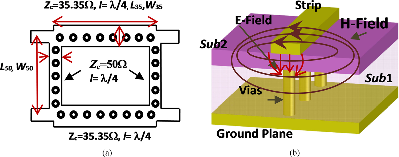
The topology of the proposed SMS coupler is presented in Fig. 1(a). The double-layer PCB is described in Fig. 1(b). The lower substrate layer Sub1 is Rogers RO4003 having h1 = 0.813 mm, εr1 = 3.55 and tan(δ1) = 0.0027 while the upper substrate layer Sub2 is Rogers RO4403 having h2 = 0.29 mm, εr2 = 3.4 and tan(δ2) = 0.005. One row of metallic vias is embedded in Sub1 along the strips length. The presence of the via holes guarantees the concentration of the electric field in Sub2 while the magnetic field still circulates around the strip as in the classical microstrip case where no vias are included. This is illustrated in Fig. 1(b) where the electric field is captured by the via holes and the magnetic field circulates in the different media around the strip (air, Sub1, and Sub2). This separation of the electric and magnetic field lines is the origin of the slow-wave effect, as explained in [Reference Serrano, Franc, Assis, Podevin, Rehder, Corrao and Ferrari7].

Fig. 1. Schematic view of the proposed (a) SMS coupler and (b) SMS line topology.
Design, realization and measurement of SMS lines
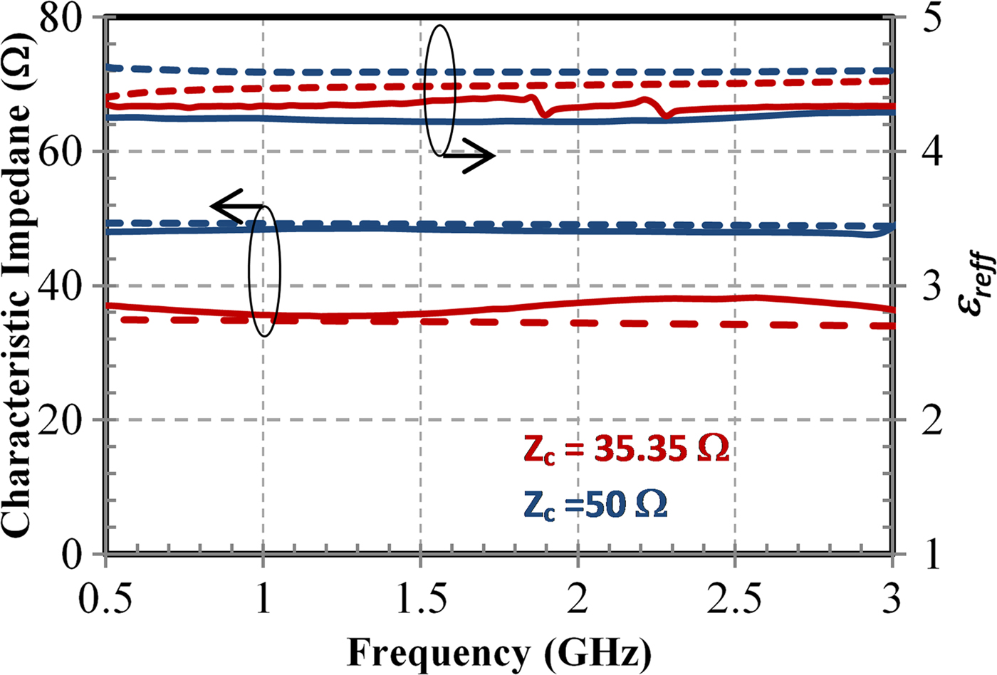
SMS lines with 35.35 Ω and 50 Ω characteristic impedances were designed, fabricated, and tested. Electromagnetic simulations were carried out using Ansys HFSS [8]. For each SMS line, three different lengths (16, 32, and 64 mm) were considered in order to extract their electrical characteristics. The extraction was done using the Two-line method [Reference Mangan, Voinigescu, Yang and Tazlauanu9]. The measurements were done using a vector network analyzer ANRITSU 37369A. The 35.35 Ω SMS line presents a width of 2.9 mm as compared with 4 mm corresponding to its classical MS counterpart designed using the same substrate stack. On the other hand, the 50-Ω SMS line has a width of 1.4 mm as compared with 2.55 mm for a classical 50-Ω MS line. Note that the SMS strip widths are thinner than for microstrip lines. This is a result of the additional capacitive effect due to the proximity of metallic vias and signal strip. Only one via row is used longitudinally underneath the strip of the SMS line because the electric field will be sufficiently captured. Inserting more via rows have drawbacks such as increase in the complexity of the structure, the cost of fabrication, and the insertion loss. This is demonstrated in [Reference El-Halabi, Issa, Pistono, Kaddour, Abou-Chahine and Ferrari10]. The simulated and measured characteristic impedance Z c, as well as the effective relative dielectric constants ε reff for both SMS lines are compared in Fig. 2. A good agreement is found between simulated and measured values of Z c and ε reff. For a SMS line having a characteristic impedance of 35.35 Ω, the measured value of ε reff at 2.45 GHz is 4.3 while the value of ε reff of its MS counterpart is 2.8, leading to a slow-wave factor equal to  $\sqrt {\varepsilon _{reff - SMS}/\varepsilon _{reff - MS}} = \sqrt {4.3/2.8} = 1.23$. The measured ε reff is 4.2 for the 50-Ω SMS line and 2.6 for its MS counterpart, leading to a slow-wave factor equal to 1.27.

Fig. 2. Characteristic impedance and relative effective dielectric constant of the SMS lines (---Simulated, —Measured).
Branch-line coupler: design and measurements
Classical microstrip branch-line coupler
A classical branch-line coupler based on microstrip lines was designed and fabricated at 2.45 GHz, to serve as a reference. Figure 3 shows the simulated and measured S-parameters of the designed MS branch-line coupler. Measurements were done with vector network analyzer KEYSIGHT N5222A using electronic calibration. A 90-MHz shift of the center frequency is noticed due to a slight variation of the upper substrate layer parameters used in fabrication. At 2.36 GHz (location of the maximum of coupling coefficient and minimum insertion loss), the measured insertion loss and coupling coefficient are equal to 3.6 and 3.8 dB, respectively, leading to an amplitude imbalance (S 13-S 12) equal to 0.2 dB. The average insertion loss, defined as [3 dB + (S 12 + S 13)/2], is equal to −0.7 dB. The measured return loss and isolation factor are equal to 70 and 71 dB, respectively. The classical MS coupler size is 26.1 × 22.95 mm2 with lines lengths L 35Ω = 19.2 mm and L 50Ω = 22.3 mm.
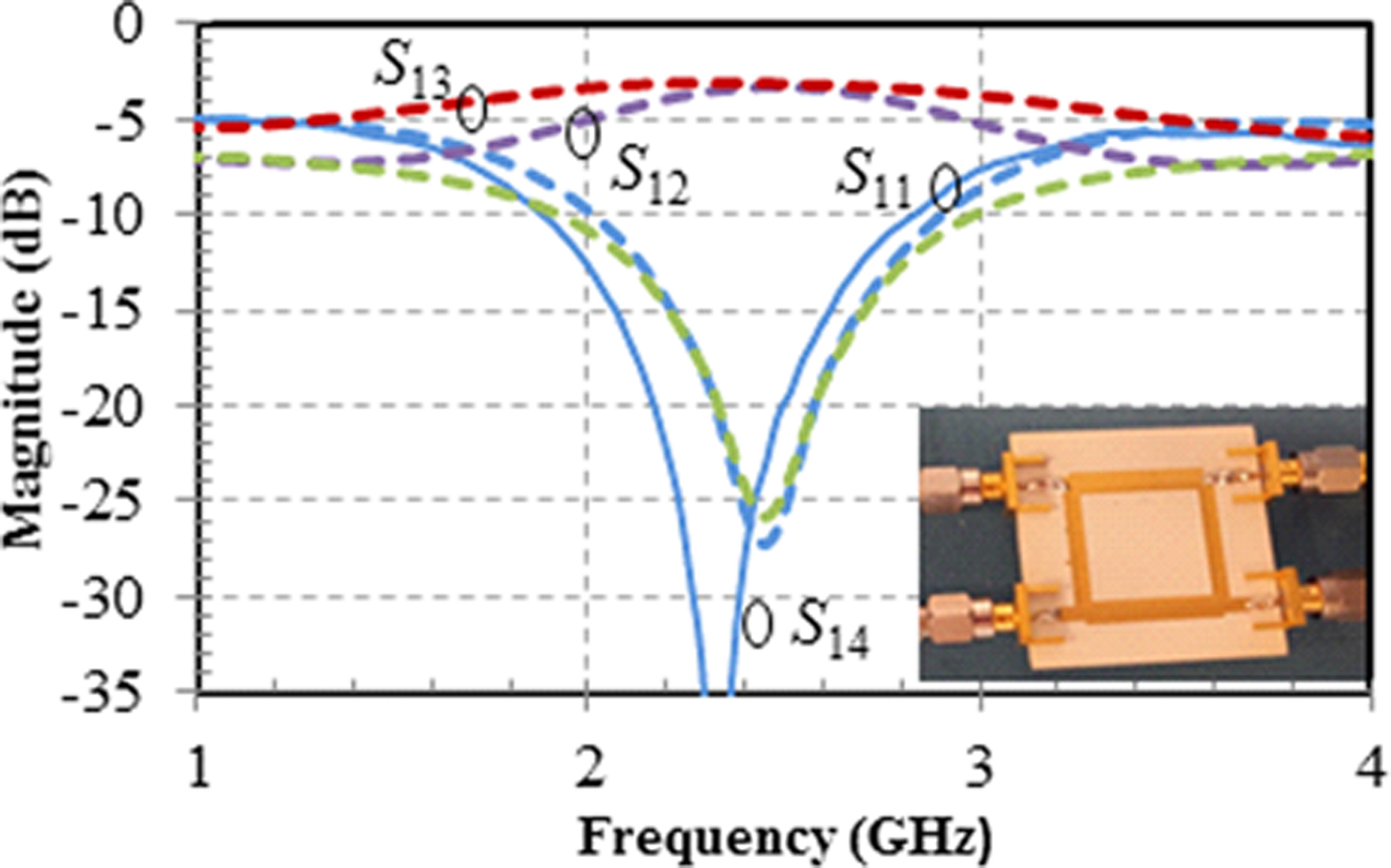
Fig. 3. Classical MS branch-line coupler S-parameters (----Simulated, —Measured).
SMS branch-line coupler
The 35.35-Ω and 50-Ω SMS lines presented in the section “PCB slow-wave microstrip” were used for the design and fabrication of the proposed SMS coupler. Final optimization of the SMS lines length was needed to get a satisfying coupler response, due to T-junctions parasitics: L 35Ω = 15.6 mm and L 50Ω = 17.0 mm. Note that the optimization of the T-junctions is much simpler with SMS lines, since the strip of SMS lines is smaller, leading to much minor parasitics.
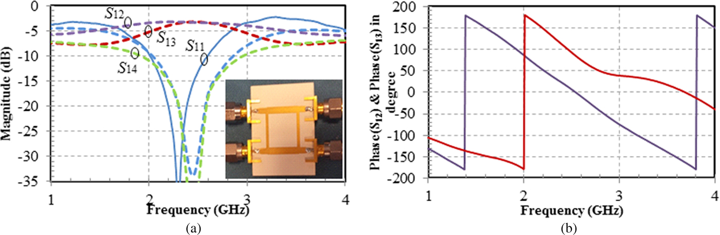
The measured magnitude and phase responses of the fabricated SMS coupler are shown in Figs 4(a) and 4(b), respectively. Here again, a shift of 90 MHz of the working frequency is noticed. The measured values of the insertion loss S 12, coupling coefficient S 13, return loss S 11, and isolation S 14 at 2.36 GHz are 2.9, 3.2, 25.5 and 27.5 dB, respectively. The amplitude imbalance is −0.3 dB, which is comparable with the reference MS coupler. The average insertion loss is equal to −0.05 dB, i.e. much lower than the MS coupler. The phase difference between the output ports is 91° at 2.36 GHz, as shown in Fig. 4(b). The surface area of the miniaturized coupler is 17 × 19.9 mm2, thus presenting a surface miniaturization of 43% as compared with the MS coupler.

Fig. 4. S-parameters of the SMS branch-line coupler: (a) Magnitude response, (b) Phase response (---- Simulated, —Measured).
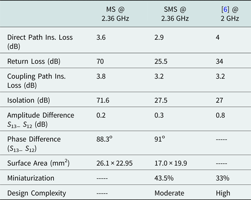
Table 1 presents a comparison between the measured characteristics and the size of both MS and SMS couplers. The phase difference between S 13 and S 12 is 88.3° for the MS coupler and 91° for the SMS coupler, respectively, at the working frequency of 2.36 GHz. Table 1 also presents a comparison between the SMS couplers realized in this work and that presented in [Reference Coulombe, Nguyen and Caloz6]. A significant improvement in both size reduction and electrical performance is noticed, accompanied with a reduction in circuit complexity.
Table 1. Coupler Comparison

Conclusion
A miniaturized and high-performance branch-line coupler based on slow-wave microstrip lines was presented. Conventional and miniaturized couplers were designed at 2.45 GHz. The proposed slow-wave microstrip technology allowed a size reduction of 43% as compared with classical microstrip coupler, by improving too its electrical performance since insertion loss is reduced by 0.7 dB for the slow-wave based coupler as compared with the microstrip classical one. This size reduction highlights the potential of slow-wave microstrip lines for the realization of RF miniaturized circuit devices, without any specific design effort as compared to classical microstrip lines. As compared with [Reference Coulombe, Nguyen and Caloz6], the technology is simpler, leading to a simpler design, and ultimately better electrical performance.
Acknowledgement
This work was partially supported by the franco-lebanese program “Partenariat Hubert Curien” CEDRE and by the French program Rhône-Alpes International Cooperation and Mobilities (CMIRA).
 Heba Alhalabi received her Ph.D. degree in Communication and Electronics Engineering from Beirut Arab University, Beirut, Lebanon. She is currently a faculty member in the engineering department of Beirut Arab University. Her current research interests include miniaturization of RF devices
 Hamza Issa received his B.E. in Electrical Engineering – Communication and electronics section from Beirut Arab University, Beirut, Lebanon. He finished his Master Degree in Radiofrequency and Optoelectronics from Grenoble University, France in 2006. He was awarded the Ph.D. degree from Joseph Fourier University, France, in 2010. In 2010, he held a temporary lecturer and research assistant position in Grenoble University, Grenoble, France. In 2011–2012 he had a postdoctoral position with Demokritos, Greece, and continued as a temporary lecturer and research assistant in Grenoble University. Since 2013 he has been an associate professor with the Beirut Arab University, Lebanon. His research interests focus on design, characterization, and modeling of passive microwave devices and antennas.
 Florence Podevin received the Ph.D. degree in Microelectronics from the “Université des Sciences et Technologies de Lille, France, in 2001. Between 2001 and 2016, she has been an assistant professor at the Grenoble Institute of Technology, part of the University Grenoble Alpes, Grenoble, France. She is now an associate professor. In 2001, she joined the IMEP-LAHC, Grenoble, France. She was initially involved in projects concerning optical control of microwave devices and periodic structures filtering. She recently joined the Radio Frequency Integrated Circuits Lab where she is currently involved under the framework of RF and Millimeter-Wave projects. She has authored or co-authored more than 100 papers published in international journals or conferences. She co-holds two patents. Her main research interest concerns tunable and miniaturized devices, such as phase shifters, power dividers, couplers based on high performing transmission lines as slow-wave ones, at mmw frequencies, in silicon technologies or on advanced substrates dedicated to millimeter waves.”
 Philippe Ferrari received the Ph. D. degree from the “Institut National Polytechnique de Grenoble” (INPG), France, in 1992, with honors. Since 2004, he is a professor at the University Grenoble Alpes, Grenoble, France. His main research interest concerns tunable and miniaturized devices, such as filters, phase shifters, matching networks, couplers, power dividers, and VCOs. These devices are developed in many technologies, PCB, CMOS/BiCMOS, and nanowires, at RF and mm-wave frequencies. He has worked towards the development of slow-wave CPW, and developed new topologies of slow-wave transmission lines, based on microstrip lines and SIWs, respectively. He is author or co-author of more than 190 papers published in international journals or conferences, and co-holder of six patents. He is an IEEE senior member, a member of the Editorial Board of the International Journal on RF and Microwave Computer-Aided Engineering (Wiley), and an Associate Editor of the International Journal of Microwave and Wireless Technologies (EuMA).