


I. INTRODUCTION
Nowadays, the companies working in the communication market need to constantly increase the number of customer's services to boost their offers. From the engineering point of view, to face this challenge, it becomes mandatory to increase the data rate transmission and thus to use digital modulated signals like CDMA-2000, WCDMA, OFDM, etc. [Reference Steer1]. Therefore, due to the high peak-to-average power ratio (PAPR) shown by such signals, the RF transmitter, and in particular the power amplifier (PA), has to be able to amplify signals with significant time-varying envelope, maintaining its efficiency and linearity levels as higher as possible for the whole signal dynamic range. Consequently, to fulfill the increasing market requests, the research activities have been focused on different solutions to develop more efficient PAs able to operate with time-varying envelopes signals. In these cases, in fact, the instantaneous efficiency, typically optimized for the peak envelope power level, becomes less significant as compared with the average efficiency, defined as the ratio between average output power and average supplied DC power [Reference Raab2–Reference Kennington4]. Therefore, the key issue in modern PA design is to develop techniques capable to improve the average efficiency [Reference Kennington4]. Clearly, the latter depends on both the PA instantaneous efficiency and the signal probability density function, i.e. the relative amount of time spent by the input signal envelope at different amplitudes. Therefore, to obtain high average efficiency when time-varying envelope signals are used, the PA should work at the highest efficiency level in a wide range of its output (i.e. input) power. This requirement could be satisfactorily fulfilled by the Doherty power amplifier (DPA), as shown in Fig. 1, where its theoretical efficiency behavior is reported [Reference Doherty5, Reference Colantonio, Giannini, Giofrè and Piazzon6]. The region with almost constant efficiency identifies the DPA output back-off (OBO) range, and it is fixed according to the PAPR of the signal to be amplified.

Fig. 1. Theoretical efficiency behavior of a DPA.
On the other hand, the requirement for high power, for instance in base station applications, necessitates transistors with high power density, large breakdown voltage, and high thermal capability. In this context, the research investigations on materials with large energy gap brought to the development of III–V devices with very attractive characteristics [Reference Mishra, Shen, Kazior and Yi-Feng7, Reference Trew8]. In particular, the combination of the wide bandgap property of GaN technology and the availability of the AlGaN/GaN heterostructure brought the GaN high electron-mobility transistors (HEMTs) to be a serious candidate to replace actual solid state devices in application where high-power and high-efficiency operation is needed [Reference Mishra, Parikh and Wu9]. With this combination, in fact, high voltage, high current, and low on-resistance can be simultaneously achieved. A space qualification is also expected in the near future and several efforts are concentrated to improve such a strategic technology. The use of GaN allows also a strong reduction in the active area required to achieve a fixed output power level as compared with GaAs technology; thus, for instance, reducing also the combining structures and their related unavoidable losses [Reference Mishra, Parikh and Wu9].
In this contribution, the possible benefits coming from both the use of GaN HEMT technology and the implementation of DPA architecture in the next generation of wireless systems are evaluated. In particular, the capabilities and the relevant drawbacks of a GaN HEMT technology [Reference Peroni10] when designing DPAs are highlighted throughout several experimental results. Moreover, a deep discussion of the DPA's design guidelines is also presented.
II. GaN HEMT device
The active devices used in the following have been fabricated by SELEX Sistemi Integrati with their standard Co-planar Waveguide GaN-HEMT processing technology, based on a GaN/AlGaN/GaN epitaxial layer structure deposited on a semi-insulating SiC substrate [Reference Peroni10]. Device fabrication technology is based on Stepper lithography, except for the Gate definition, based on electron beam lithography (EBL). Drain and source ohmic contacts were obtained by metal deposition (Ti/Al/Ni/Au) and subsequent high-temperature rapid thermal processing (over 850 °C). Subsequently, the wafer surface is passivated using SiN plasma-enhanced chemical vapor deposition for surface protection, while the active device isolation is achieved by means of fluorine ion implantation. The Gate electrode is then formed basing on a double step EBL process, to provide a “Γ” shape to the Gate metallization with a length of LG = 0.5 µm. The deposition of SiN layer has been optimized to minimize the carrier trap concentration at the interface with the semiconductor. Moreover, the Γ-Gate geometry has been optimized to obtain the desired compromise between device breakdown and high-frequency RF gain [Reference Peroni10]. The wafer fabrication is finally completed with Ti/Pt/Au overlay interconnection and Au-plated for lines, pads, and air bridges to provide the discrete devices in coplanar system. Figure 2 shows a photograph of the active device used to design the all DPAs reported in the following.

Fig. 2. Photo of the active device used.
III. Design guidelines for DPA
The modern DPAs are usually implemented by a proper combination of two active devices designed to operate as a class AB (Main) and as a class C (Auxiliary) power stage, respectively. Both PAs are connected at the output through a quarter-wave transmission line (λ/4 TLine), as shown in Fig. 3, with the aim to properly exploit the active load modulation concept performed by the Auxiliary amplifier on the Main one [Reference Doherty5, Reference Colantonio, Giannini, Giofrè and Piazzon11, Reference Colantonio, Giannini, Giofrè and Piazzon12]. Moreover, to further increase the DPA efficiency performance, harmonic tuning strategies could also be adopted [Reference Colantonio, Giannini, Giofrè and Piazzon6, Reference Kim13], while to improve its linearity a baseband digital predistortion is usually implemented [Reference Sung-Chan, Hammi and Ghannouchi14].

Fig. 3. Typical DPA architecture.
In any case, the behavioral analysis of DPA can be performed considering two different operating conditions [Reference Colantonio, Giannini, Giofrè and Piazzon11]:
– low power, i.e. before the Auxiliary device is turned on, which is referred as break point condition;
– medium power, when both devices are active, referred as Doherty region.
In order to infer useful design relationships and guidelines, simplified models are assumed for the DPA elements. In particular, the passive components (λ/4 TLine and power splitter) are assumed to be ideally lossless, while for the active device (in the following assumed as a FET type) an equivalent linearized model is assumed, as shown in Fig. 4. It is represented by a voltage-controlled current source, while for simplicity any parasitic feedback elements are neglected and all the other ones are embedded in the matching networks.

Fig. 4. Simplified model of the active device.
The device output current source is described by a constant transconductance (g m) in the saturation region, while an ON resistance (R ON) is assumed for the ohmic region, resulting in the output I–V characteristics shown in Fig. 5.

Fig. 5. I–V output characteristics of the simplified model.
In the DPA design, the device parameters to be considered are the maximum achievable output current (I Max), the constant knee voltage (V k), and the pinch-off voltage (V p).
Usually, accounting for the PAPR of the system in which the DPA will be used, its design starts fixing the OBO value, defined as

where the subscripts are used to refer to the entire DPA or to the single amplifiers (Main and Auxiliary respectively). Moreover a parameter x (0 ≤ x ≤ 1) is used to identify the dynamic point in which those quantities are considered. In particular x = 0 identifies the quiescent state, i.e. when no RF signal is applied to the input, while x = 1 identifies the saturation condition, i.e. when the DPA reaches its maximum output power level. Similarly, x = x break identifies the break point condition, i.e. when the Auxiliary amplifier is turned on.
Assuming a bias voltage V DD, and assuming a tuned load configuration for both amplifiers, i.e. a short circuit loading condition for the impedances at harmonic frequencies, the following consideration can be done:
– the drain voltage amplitude of the Main device is equal to V DD − V k both for x = x break and x = 1 as also highlighted by the load curves A and C reported in Fig. 6, respectively;
– the same amplitude value is reached by the drain voltage of the Auxiliary device for x = 1, as shown by the load curve “C” in Fig. 6.
Consequently the output powers delivered by the Main and Auxiliary amplifiers in such peculiar conditions become
where the subscript “1” is added to the current in order to refer to its fundamental component.
Now, exploiting the constitutional equation of the output λ/4 TLine and above all, remembering that the current on one side is a function of the voltage on the other side only (i.e. V DD − V k that is constant in the Doherty region), it is possible to write [Reference Colantonio, Giannini, Giofrè and Piazzon11]
where α defines the ratio between the currents of the Main amplifier at x = x break and x = 1. Moreover, considering the matching network lossless, the voltage V L is the one across R L and its value at the saturation (x = 1) has to be equal to V DD − V K. As a consequence, the following relationship rises:

Therefore, from the previous equations it follows:
Finally, substituting (2)–(4) in (1) and accounting for (7), the following relationship can be derived:
which demonstrates that, selecting the desired OBO, the ratio between the Main amplifier currents for x = x break and x = 1 is also fixed as well as the ratio between the Main and Auxiliary fundamental current components.
Once again, since the DPA maximum output power value is usually fixed by the application requirements, it represents another constraint to be selected by the designer. Such maximum output power is reached for x = 1 and it can be estimated by the following relationship:

which can be used to derive the maximum value of fundamental current component of Main device (I 1,Main|x=1), once its drain bias voltage (V DD) and the device knee voltage (V k) are fixed.
Finally, knowing the I 1,Main|x=1 value, it is possible to compute the values of R L by (6) and the required characteristic impedance of the output λ/4 TLine (Z 0) by using
which is derived assuming that the output voltage (V L) reaches the value V DD − V k for x = 1.
Clearly the I 1,Main|x=1 value depends on the Main device maximum allowable output current I Max and its selected bias point. The latter can be expressed as a percentage of the former through the following parameter:
being I DC,Main the quiescent (i.e. bias) current of the Main device. Consequently, ξ = 0.5 and ξ = 0 refer to a class A and class B bias condition, respectively, while 0 < ξ < 0.5 identifies a generic class AB bias condition.
Assuming a sinusoidal waveform for the drain current and performing a Fourier analysis is easy to demonstrate that
being θ AB the current conduction angle (CCA) of the Main output current, achieved for x = 1. Moreover, the bias point ξ and the CCA θ AB are related by the following relationship:
Manipulating (12), the value of I Max, Main, required to reach the desired maximum output power, can be estimated once the bias point ξ of the Main amplifier has been selected. In order to proper select the Main device bias point ξ reducing the AM/AM distortion, in [Reference Colantonio, Giannini, Giofrè and Piazzon12] a figure of merit namely gain linear factor (GLF) has been introduced. Figure 7 shows the values of ξ, which theoretically assures the best GLF, as a function of the selected OBO. This design chart provides a guideline to select the proper ξ value, having fixed the desired OBO of the DPA.

Fig. 6. Evolution of the load curves for both DPA active devices.

Fig. 7. Values of ξ assuring GLF = 0, as a function of the OBO.
The procedure followed to find the design parameters of the Main device can also be applied to determine the correspondent values of the Auxiliary one. In particular, it is possible to demonstrate that the final CCA of the Auxiliary device (θ C) is a function of x break value only [Reference Colantonio, Giannini, Giofrè and Piazzon6]:
Thus, once θ C is known, the maximum current of the Auxiliary device (I Max,Aux) can be easily calculated by using (12), replacing θ AB = θ C and the subscript Main with Aux, since the value of I 1,Aux|x=1 should fulfill (7).
Moreover, to assure the right turning on condition of the Auxiliary amplifier, its output current has to become greater than zero at x = x break. Consequently, to evaluate the x break value, the following transcendental equation has to be numerically solved:
It is obtained by replacing the Fourier expressions of the fundamental current component of the Main device in the definition of the parameter α given by (5). As previously highlighted, the value of x break is calculated once the OBO (i.e. α) and the Main device bias point (i.e. ξ) have been fixed.
To determine the Auxiliary device bias condition, a “virtual” bias current I DC,Aux can be defined, which schematizes the actual bias condition (gate voltage for FET devices) required to properly control its turning on condition. In particular, known the I Max,Aux and the corresponding CCA θ C, the (negative) “virtual” bias current can be derived:
The latter has been derived imposing that the overall Auxiliary current is equal to zero at the break point [Reference Colantonio, Giannini, Giofrè and Piazzon11].
Figure 8 reports the behavior of the ratio I Max,Aux/I Max,Main as a function of OBO and for different ξ values. From the designer point of view, the maximum currents ratio can be used as a useful information to choice the proper device periphery or scaling factor.

Fig. 8. Ratio between Auxiliary and Main maximum currents.
In order to complete the DPA design, the input power splitter has to be dimensioned. To this purpose, the following boundary conditions have to be addressed:
– when the Main device reaches the break point condition, the Auxiliary has to be turned on;
– afterwards, the Auxiliary device has to be driven into its conduction state to achieve the I Max,Aux value, while assuring that the Main device simultaneously reaches its maximum current I Max,Main.
In Fig. 9, the computed values for ΛAux (i.e. the amount of power delivered to the Auxiliary device with respect to the total input power) is reported, as a function of OBO and ξ parameters, assuming for both devices the same values for g m and R in.

Fig. 9. Λ Aux behavior as a function of OBO and ξ.
Figure 9 highlights that large amount of input power has to be sent to the Auxiliary device, requiring an uneven power splitting. This aspect dramatically affects the overall gain of the DPA, which typically becomes 5–6 dB lower if compared with the gain achievable by using a single amplifier only.
Nevertheless, it has to remark that this largely unbalanced splitting factor has been inferred assuming a constant g m for both devices. Such approximation is sufficiently accurate in the saturation region (x = 1), while becomes unsatisfactory for low power operation (i.e. small signal). Thus, if the bias point of Main amplifier ξ is selected roughly lower than 0.2, the predicted gain overestimate the gain in actual experimental conditions.
Once the DPA design parameters have been settled, closed form equations for the estimation of the achievable performances can be obtained, as reported in [Reference Colantonio, Giannini, Giofrè and Piazzon11].
An example of the inspected theoretical performance of a DPA designed to fulfill 6 dB of OBO and 4 W as maximum output power is shown in Fig. 10.

Fig. 10. Theoretical performances of a DPA.
Due to the different bias condition of both devices, the gain of the overall DPA shows a non-constant behavior, especially in the Doherty region. This results in a difference between the selected OBO and the input back-off, which generates an AM/AM distortion in the overall DPA. As already discussed, its value can be drastically reduced by selecting the Main bias point following the GLF (Fig. 7).
In order to further clarify the DPA behaviors, Fig. 11 shows the fundamental drain currents and voltages for both Main and Auxiliary devices. These behaviors can be used in the design flow to verify whether the DPA operates in a correct way. In particular, the attention has to be focused on the Main voltage, which has to reach, at the break point (x break), the maximum achievable amplitude (10 V in this example) in order to maximize the efficiency. Moreover, the Auxiliary current can be used to verify that the device is turned on at the right dynamic instant. Finally, the designer has to pay attention if the Auxiliary current reaches the expected value at the saturation (x = 1), in order to perform the desired modulation of the Main resistance.
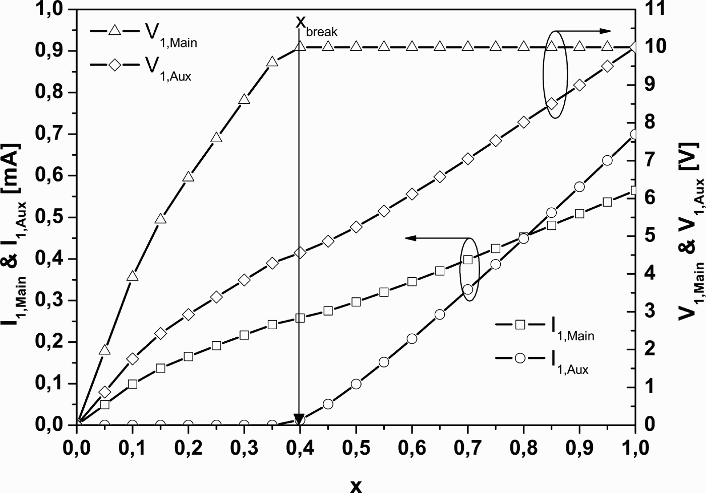
Fig. 11. Fundamental current and voltage components of Main and Auxiliary.
The extension of the analysis here reported, including also harmonic tuning strategies for the Main amplifier, and in particular a class F approach, was also discussed in [Reference Colantonio, Giannini, Giofrè and Piazzon6]. Similarly, advanced solutions based on different output drain voltage supplies or accounting on for the RON resistance were also proposed in ref. [Reference Colantonio, Giannini, Giofrè, Piacentini and Piazzon15].
IV. Experimental results using GaN HEMT
As mentioned in the introduction, the combination of DPA architecture and the GaN technology should allow to satisfy the power, efficiency, and linearity requirements of the next generation of wireless systems.
The DPA relationships reported previously represent the basic guidelines allowing a dramatically reduction in the “time to market” design, since all the design parameters and the achievable performance are known once the active device technology is chosen.
The derived formulation has been used to design several DPAs using a GaN HEMT technology provided by Selex-SI. All circuits are realized in hybrid technology for UMTS applications (center frequency 2.14 GHz) and have been designed in order to obtain 6 dB of OBO (α = 0.501).
The adopted active device, for both Main and Auxiliary amplifiers, is a GaN HEMT, 10 × 100 µm gate fingers, 0.5 µm gate length, resulting in 1 mm of gate periphery. It has been in house characterized by using both static DC and pulsed I–V measurements, together with S-parameters measurements. A nonlinear model has been developed and validated through load pull measurements by using the equivalent circuit approach proposed in [Reference Cabral, Pedro and Carvalho16]. The resulting output characteristics are depicted in Fig. 12.

Fig. 12. Output DC I–V characteristics of the used active device.
From this figure, it can be easily inferred a knee voltage of V k = 2.4 V, a pinch-off and built-in voltages of V p = −6.5 V and V bi = 0 V, respectively, and a maximum output current of I Max = 0.93 A. Moreover, the device presents a power gain estimated by simulation for a class A bias condition of G A = 14.9 dB, for the selected drain bias voltage V DD = 15 V.
Once the limits of the device active region have been identified, using the derived formulas it is very easy either to determine the DPA design parameters or to evaluate the achievable performance. In this case, since only one periphery was available, the design started fixing the maximum current of the Auxiliary device equal to I Max = 0.93 A.
The first example is a tuned load DPA (TL-DPA), reported in Fig. 13, implementing short circuit condition at harmonic frequencies for both active devices.

Fig. 13. Photo of the realized GaN TL-DPA.
The impedances seen across the intrinsic nonlinear current sources of both Main and Auxiliary devices, obtained through a full nonlinear simulation, as compared with the theoretical ones inferred from the simplified analysis, are depicted in Fig. 14.

Fig. 14. Intrinsic load impedances of Main and Auxiliary devices.
As can be noted, in this kind of GaN device, the intrinsic output resistance is not negligible and its effect has to be accounted in the load modulation phenomenon. Consequently, for the Main device it becomes critical to simultaneously fulfill the theoretical load conditions at the break and at the saturation points. If the load value at break point is fulfilled (in this case 77 Ω), then in saturation the resulting load becomes higher than the theoretical expected (i.e. 43 Ω instead of 38.5 Ω), so reducing the current swing and the final achievable output power. On the contrary, fulfilling the condition in saturation (38.5 Ω) the final maximum output power can be achieved, while the load value at the break point will be lower as expected (i.e. 84 Ω instead of the required 77 Ω). Clearly the second solution is most convenient in terms of achievable output power, and thus was preferred in this example, as evidenced in Fig. 14.
The comparison between the continuous wave (CW) measured performance and the simulated ones are reported in Fig. 15.

Fig. 15. Measurements of the realized TL-DPA compared with the simulations.
In the obtained 6 dB of OBO, an average drain efficiency of 40.7% is achieved with 3 W of saturated output power.
In Fig. 15 are also reported the comparisons of the DC currents of both devices. It is interesting to highlight the role could have this kind of measurement in an experimental evaluation of DPA behavior. Since the DC currents supplied to the two devices can be easily measured, their comparisons with the expected values can put into evidence how close the realization of the amplifier and the original design are. Moreover, both the bias level of the Main amplifier and the turning on point of the Auxiliary device can be properly adjusted to overcome two practical issues: the uncertainty on the actual value of device pinch-off voltages and the lack of information related to the behavior of the Auxiliary device in its off condition.
The second DPA was designed implementing a class F harmonic termination for the Main device (F-DPA), based on the same active devices [Reference Colantonio, Giannini, Giofrè and Piazzon6]. This approach was useful to highlight which are the differences in terms of design relationships and expected performances when a tuned load or class F harmonic termination is used to build a Doherty amplifier. In fact, when a tuned load solution is considered, all the harmonic components of the output current are short-circuited with the aim to shape a purely sinusoidal waveform for the resulting output voltage. Conversely, in high-frequency class F approach (i.e. considering only the first three harmonics), the harmonic components of the device output current are properly terminated in order to square the resulting output voltage, i.e. in order to generate the voltage harmonic components with suitable phase relationships and amplitude ratios [Reference Colantonio, Giannini, Leuzzi and Limiti17]. Moreover, to have a coherent comparison between the two different approaches (tuned load and class F), the design and the realization of a 2.14 GHz class F DPA has been performed by using for both the Main and the Auxiliary amplifiers the same active devices used in the TL DPA design already presented in [Reference Colantonio, Giannini, Giofrè and Piazzon12].
The photo of the realized class F DPA is reported in Fig. 16.

Fig. 16. Photo of the realized GaN class F-DPA.
The CW measured performance is reported in Fig. 17 compared with the simulated ones. As can be seen, in the Doherty region, an average drain efficiency of 50% has been registered while achieving a saturated output power of 3.2 W.

Fig. 17. Comparison between the simulated and measured performances of the class F-DPA.
Moreover, Fig. 18 shows the comparison between the measured performances of the TL-DPA and the class F-DPA as a function of the output power. As can be noted, the class F-DPA shows a drain efficiency roughly 15% higher than the efficiency of the TL-DPA, as expected with a class F approach [Reference Colantonio, Giannini, Leuzzi and Limiti17].

Fig. 18. Comparison between the measured performances of the TL-DPA and the class F-DPA.
The last DPA here reported has been realized implementing a different solution to design a more compact uneven TL-DPA. The proposed solution allows the possibility to dramatically reduce the size of the resulting DPA, by using a single output matching network for both Main and Auxiliary devices, without limiting the DPA operating criteria [Reference Colantonio, Giannini, Giofrè and Piazzon18]. A photo of the realized DPA is reported in Fig. 19.

Fig. 19. Photo of the realized DPA.
This DPA was also tested with complex modulation, and in particular using a 3GPP WCDMA signal at 2.14 GHz with 4 MHz of relative bandwidth and 7.4 dB of PAPR. Figure 20 shows the input and output power spectral density at 27.7 dBm of average input power. As can be seen from the picture, the power in the adjacent channel is roughly 20 dB lower than the power in the operating band.

Fig. 20. Measured output spectra for 3GPP WCDMA signal.
V. Conclusion
In the present paper, the features of GaN HEMT technology and DPA architecture have been investigated, as a possible answer for the requirements of the next generation of wireless systems. In particular, the attention has been focused on the capabilities and the relevant drawbacks of a GaN HEMT technology when designing DPAs. A discussion of the DPA's design guidelines has also been presented through the realization of three prototypes implementing different design solutions and working at 2.14 GHz. The first example was a tuned load DPA which showed an average drain efficiency of 40.7% with 3 W of saturated output power in the obtained 6 dB of OBO. The second DPA was designed implementing a class F harmonic termination for the Main device, based on the same active devices. In this case, the relevant differences between the two approaches have been reassumed, showing an improvement of roughly 15% in output power and efficiency behavior of class F DPA towards TL DPA. The last DPA has been realized implementing a single output matching network for both Main and Auxiliary devices, which allows a relevant reduction in the size of the resulting DPA, without deteriorating the DPA performances.
 Paolo Colantonio was born in Roma, Italy on March 22, 1969. He received the degree in electronic engineering from University of Roma “Tor Vergata” in 1994 and the Ph.D. in Microelectronics and Telecommunications in 2000. In 1999 he became a Research Assistant at the same university, where since 2002 he has been a Professor of Microwave Electronics. His main research activities are in the field of nonlinear microwave circuit design methodologies, nonlinear analysis techniques and modeling of microwave active devices.
 Franco Giannini was born in Galatina (LE) Italy, on November 9, 1944. He received the Electronics Engineering (summa cum laude) from the University of Roma “La Sapienza”, Rome, Italy, in 1968. Since 1980, he has been a Full Professor of applied electronics with the University of Rome Tor Vergata, Rome, Italy. Since 2001, he has been an Honorary Professor with theWarsaw University of Technology (WUT), Warsaw, Poland. He has been involved with problems concerning modeling, characterization, and design methodologies of linear and nonlinear active microwave components, circuits, and subsystems, including monolithic microwave integrated circuits (MMICs). He is a consultant for various national and international industrial and governmental organizations, including the International Telecommunication Union and the European Union. He has authored or coauthored over 340 scientific papers. Prof. Giannini is a member of the Board of Directors of the Italian Space Agency (ASI). He is president of the GAAS Association. He has also been a member of numerous committees of international scientific conferences. He was the recipient of the Doctor Honoris Causa degree from the WUT in 2008.
 Rocco Giofrè was born in Vibo Valentia (Italy) on August 13, 1979. He received the electronic engineering degree (M.S. Eng.), summa cum laude, from University of Roma “Tor Vergata” in 2004 and the Ph.D. degree in space systems and technologies in 2008 from the same University. He is presently a researcher at the Electronics Engineering Department of the University of Roma “Tor Vergata”. His research interests include RF power amplifier theory, design and test, linearization techniques, and efficiency improving techniques. He was recipient of the 2005 Young Graduated Research Fellowship presented by the Gallium Arsenide application Symposium Association (GAAS) and of the best paper award at the 2th EuMIC Conference in 2007. He has authored or coauthored over 50 scientific papers.
 Luca Piazzon was born in Frascati, Italy, in 1982. He received the B.S. degree in Electronic Engineering from Tor Vergata University, Rome, Italy, in 2007. Currently, from November 2008, he is a Ph.D. Student at the Tor Vergata University. His current research interests include RF power amplifier theory, design and test, linearization techniques, and efficieny improving methodologies.


