


I. INTRODUCTION
AlGaN/GaN high electron-mobility transistors (HEMTs) show better power performances at a given frequency than lower band-gap materials. At material level, piezoelectric effects in the GaN structure lead to the presence of fixed charges at interfaces, giving rise to a two-dimensional electron gas with an electron density larger than that created for example in GaAs HEMTs using intentional doping. The large band-gap of 3.4 eV results in a high breakdown field of 3 MV/cm and allows an increase in bias voltage and power by a factor of at least five compared to low band-gap technologies [Reference Wu, Kapolnek, Ibbrtson, Parikh, Keller and Mishra1–Reference Couturier4]. This high breakdown field combined with a high electron saturation velocity, as well as a high carrier density and mobility through the AlGaN/GaN heterostructures, lead to many developments on this technology. GaN HEMTs were initially developed for power applications, the thermal conductivity of GaN at 300 K of 190 Wm−1K−1 and that of silicon carbide (SiC) of 400 Wm−1K−1, allowing a good dissipation of the heat generated in the channel. These good thermal properties promoted epitaxial structures grown on SiC substrate for power applications. Nevertheless, the noise factor and the robustness to high levels of overdrive lead such technology to be evaluated in other functions [Reference Kobayashi, Chen, Smorchkova, Tsai, Wojtowicz and Oki5–Reference Mancuso, Gremillet and Lacomme8]. At the emission part, power switches are studied as an alternative solution to circulators to reduce size and weight. For the reception, robust low-noise amplifiers (LNAs) should allow module designers to move the limiter behind the amplifier. This should reduce the noise budget of the reception chain and thus increase the dynamic of reception. Mixers are also studied for good inter-modulation performances, noise characteristics, and linearity [Reference Sudow9]. In this work, we present an overview of the circuits realized at Alcatel-Thales 3–5 lab last years. High-power amplifiers in L- and X-bands and broadband 6–18 GHz are presented. Hybrid or MMIC amplifiers were developed taking into account the availability of via-holes in through the SiC substrate and frequencies of operation. Results on LNAs and power switches are also shown. All these developments contribute to prepare the next generation of Tx-Rx front-end modules based on GaN material.
II. MATERIALS
AlGaN/GaN HEMT epitaxial layers are grown on an SiC substrate using low-pressure metal organic chemical vapor deposition. Mercury probe C–V measurements show a typical sheet carrier density of 1.1013 cm−2. TLM (Transmission line measurements) measurements present a mean sheet resistance of 490 Ω per square for an aluminum fraction of 28% in the 22-nm-thick AlGaN layer. Figure 1 shows a cross-section of such typical layer structure.

Fig. 1. Typical layer structure of AlGaN/GaN HEMT.
III. DEVICE TECHNOLOGY
The electrical isolation of components is performed by helium implantation. Ti/Al/Ni/Au ohmic contacts are formed using a rapid thermal anneal at temperature of 900 °C. Good and reproducible contact resistances are obtained at a typical value of 0.2 Ω mm. Mo-based field-plated 0.7 µm gate length process or 0.25 µm mushroom gate process are defined by electron beam lithography to address applications from 1 to 18 GHz. Devices are passivated by depositing an SiO2–Si3N4 layer by plasma enhanced chemical vapor deposition (PECVD). Then, main electrical interconnections are made using Ti/Pt/Au metals.
MMIC production needs additional process steps. Passive elements consist in PECVD nitride MIM capacitors, NiCr resistors, and evaporated Ti/Pt/Au inductances. After frontside processing, the AlGaN/GaN heterostructure grown on SiC wafer is mounted top side down on a sapphire substrate and thinned down to 100 µm. Plasma etching via-holes technology is then used to ground the devices. Vias and backside metallization consisted in sputtered TiW/Au and Au plating. Figure 2 shows a cross-section of the main steps realized during the 0.7 µm gate length process.

Fig. 2. Cross-section of main steps of 0.7 µm gate length process.
IV. DEVICES TOPOLOGIES
Appropriate device topologies are necessary to cover applications ranging from around 1 to 18 GHz, LNAs to high-power amplifiers emitting few watts at upper frequencies to more than 100 W in S-band. For a given application, ‘pizza’ mask combining a large set of components are thus often designed in a first step to evaluate and choose the best suitable device. Trade-off between gain, power, and or input and matching has to be considered. Figure 3 shows photographs of coplanar 4 × 250 µm with coplanar accesses for typical S-band applications and microstrip 12 × 100 µm transistor dedicated to X-band.

Fig. 3. Photograph of coplanar 4 × 250 µm (left) and microstrip 12 × 100 µm power device (right).
The 4 × 250 µm devices built with the 0.7 µm gate length process exhibit a maximum drain current value at V gs = 0 V (I dss) of 0.7 A/mm at a drain voltage of 6 V. The maximum DC transconductance g m is 0.4 S/mm. Pinch-off and breakdown voltages (at 1 mA/mm of drain current) are, respectively, −3.6 and 160 V. Minimum noise factor (NF min) of the 4 × 250 µm device is 1.2 dB at 2 GHz for a V ds voltage of 10 V (Fig. 4). Power 8 × 250 µm devices under load-pull measurements demonstrate an output power of 9 W (4.5 W/mm) with 56% of power-added efficiency (PAE) and 16.5 dB of gain at 3 GHz and 40 V of drain voltage in continuous wave (CW) operating conditions.

Fig. 4. NF min of 4 × 250 µm device versus frequency in L-band at different V gs voltages (V ds = 10 V).
The 12 × 100 µm devices are based on the 0.25 µm gate length process for X-band applications. These power transistors show an I dss drain current of 1.1 A/mm (Fig. 5). Its small signal gain is 15 dB at 10 GHz at a drain voltage of 25 V and a drain current of 210 mA.

Fig. 5. Pulsed I–V characteristics of 12 × 100 µm device from quiescent point V gs = 0 V and V ds = 0 V.
Figure 6 shows the current gain cut-off frequency (F t) and maximum available power gain cut-off frequency (F mag) for 0.25 µm gate length devices with various total gate widths.

Fig. 6. F mag and F t evolution versus total gate width (V ds = 5 V, I ds = 100 mA/mm).
A typical power device of 1.6 mm presents F t and F mag values of, respectively, 18 and 35 GHz. A ratio of 2 between F t and F mag values is well conserved from elementary to power devices.
Figure 7 shows load-pull power measurements of the 1.2 mm device at 10 GHz. Measurements are performed in pulse mode with a pulse length of 10 µs with 10% of duty cycle. The device is biased at a voltage of 25 V and quiescent drain current of 290 mA. At the optimum output load impedances of 12.6 + j.9 Ω at the fundamental frequency, with 50 Ω at harmonic frequencies, the device shows a typical output power of 37 dBm (5 W) corresponding to a power density of 4.2 W/mm. The PAE is 47% and the associated gain is 11 dB.

Fig. 7. Load-pull measurement of 12 × 100 µm device (V ds0 = 25 V, I ds0 = 290 mA, F 0 = 10 GHz, 10 µs/10%).
Appropriate devices are then combined to build functions delivering more gain, more power to fulfill system requirements. LNA results, power switches, or power amplifiers presented in the present paper are based on these elementary devices and technologies performances.
V. POWER SWITCH
GaN-based power switches are studied as an alternative to circulator to save space and weight in equipments. Depending on the operating frequency and bandwidth, the trade-off between performances and compactness can be discussed and power switches seem to be more interesting for wideband than for narrow band applications. Here we present the performances of a power double pass double thru (DPDT) switch designed using 4 × 250 µm GaN transistors [Reference Piotrowicz10, Reference Jardel11]. The fours paths are identical and each one is constituted of three paralleled transistors separated by a λ/4 transmission line (Fig. 8).

Fig. 8. Power DPDT principle description.
At an input power of 42 dBm, the DPDT insertion losses are lower than 2 dB over the [Reference Wu, Kapolnek, Ibbrtson, Parikh, Keller and Mishra1–Reference Sheppard2] GHz band (Fig. 9). Isolations between the four ports are better than 50 dB.
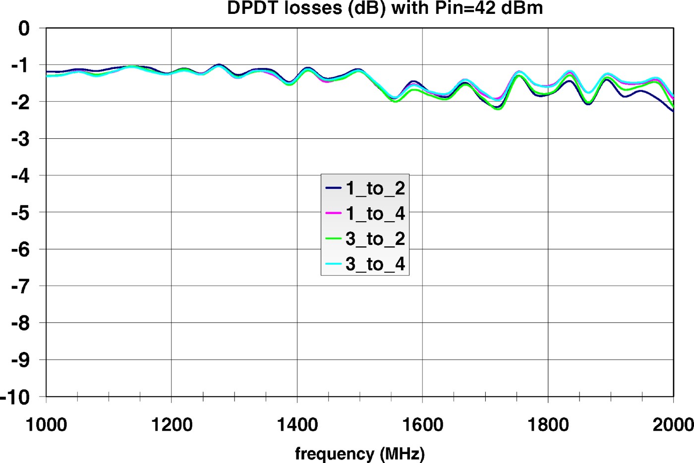
Fig. 9. Power DPDT losses with P in = 42 dBm.
The power DPDT robustness was also measured to test the maximum input power survivability. Input powers as high as 49 dBm (80 W) were necessary to destroy the switch (Fig. 10) showing the high level of power withstand by these power switches.
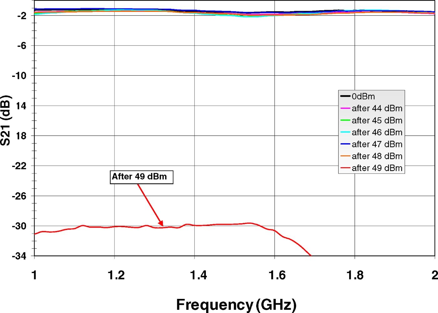
Fig. 10. Power DPDT losses versus input power ranging 44–49 dBm.
VI. LNAs
On the receive part of a transmission chain, discrete PIN diodes are often used to limit the power incoming from the antenna and protect the GaAs LNA. As for power switches, GaN-based LNAs can withstand around 10 times more power than GaAs ones allowing to suppress or move the limiter behind the LNA and improving the dynamic of the receiver. However, the noise factor of GaN HEMT has to be sufficiently low in order to have a GaN LNA noise factor comparable to the association of a GaAs LNA and a limiter.
Figure 11 shows a photograph of robust two-stage L-band LNA designed with 4 × 250 µm GaN transistors. Figure 12 shows measurements of the LNA at a quiescent bias point of V ds = 10 V and I ds = 220 mA. A noise figure of 1.7 dB and an associated gain of 22 dB are obtained.

Fig. 11. Low-noise two-stage amplifier photograph.

Fig. 12. Measured gain and noise figure of the LNA.
Return losses are better than −12 dB. An on–off switching time of 30 ns is also obtained. In order to demonstrate the robustness of the LNA to high level of overdrive, it was measured with an aggression test bench in CW mode. Input powers ranging from 22 to 38 dBm were injected at the input of the amplifier. The LNA handled input powers up to 37 dBm demonstrating the high level of overdrive capability of GaN-based LNAs.
GaN devices were also evaluated in X-band with a hybrid or MMIC approach [Reference Jansen, van Heijningen, Provenzano, Visser, Morvan and van Vliet12]. Figure 13 shows the photograph of a hybrid single-stage X-band amplifier. The amplifier is based on an 8 × 75 µm device from 0.25 µm gate length process.

Fig. 13. Hybrid single-stage X-band LNA.
Such amplifier has a small signal gain of 9 dB at 10 GHz at a quiescent current of 80 mA and V ds voltage of 10 V. The gain of the amplifier is highly reduced by the wire bondings necessary to connect the source contacts to ground but allow the device to be stabilized. Figure 14 shows the noise measurements at 10 V of V ds voltage for drain currents ranging 40–100 mA.

Fig. 14. Noise factor of hybrid single-stage X-band amplifier.
The noise factor is 1.6 dB over more than 2 GHz bandwidth with a low dependency to drain current. At the 1 dB compression point, the amplifier delivers an output power of 25.6 dBm (360 mW).
VII. HIGH-POWER AMPLIFIERS
Due to its high breakdown electrical field, high-power amplifier is the microwave function which takes more advantages of the GaN technology. These functions are developed from few Megahertz to more than 100 GHz. In this part, we present results of hybrid and MMIC high-power amplifiers up to 18 GHz.
Figure 15 shows the power stage of a broadband hybrid power amplifier in L-band and a 6 × 8 × 250 µm power die in package. The complete amplifier is constituted by two stages, each in a balanced configuration with 3 dB–90° hybrid couplers to ensure good input and output return losses. Thanks to such configuration, each stage can be measured under 50 Ω conditions separately.

Fig. 15. Photograph of the second stage of the power amplifier (95 × 70 mm2) and power die in package.
Each power die is mounted in a ceramic standard package including an R//C stabilization network at the input of each elementary 8 × 250 µm device of the power die. This network also contributes to reduce the gain ripple in the bandwidth. The two-stage amplifier was measured at a drain voltage of 18 V and a total quiescent current of 2.8 A. Measured S11 and S22 are below −15 dB in the 1–2 GHz band. The small signal gain S21 is 22.2 dB. Amplifiers were then measured under CW large signal operating conditions. The backside temperature was maintained at 25 °C. Figure 16 shows the results of the amplifier over the [Reference Wu, Kapolnek, Ibbrtson, Parikh, Keller and Mishra1–Reference Sheppard2] GHz frequency band. At an input power of 19.5 dBm, the measured output power is 42 dBm (16W) with a PAE better than 32%. At 1.2 GHz, the output power reaches 44.5 dBm (28 W) with a PAE of 40% and a gain of 25 dB. The drain current rises from 2.8 up to 4 A.

Fig. 16. Output power, PAE, and gain over the 1–2 GHz frequency band (P in = 19.5 dBm).
Each stage was separately characterized for different backside temperatures ranging [0–75] °C. The power stage shows a power variation between 0.015 and 0.02 dB/°C over the frequencies and temperatures ranges. Thermal simulations were performed to calculate a maximum channel temperature of 140 °C at a backside temperature of 50 °C. Due to the AB class of operation, the channel temperature was at its maximum at the quiescent point for low input power.
Electrical robustness was also evaluated. It consisted on presenting at the output of the amplifier different reflection coefficients from 0 (50 Ω load) to 0.7 with eight different phases to describe a complete circle in the Smith chart (Fig. 17). After each set of measurements, the first load was re-measured in order to detect degradations. No change in performances was seen thanks to the back-off took on V ds voltage for such operating conditions. Figure 18 shows the load lines described by one device at the intrinsic current source. Blue curves represent load lines described under 50 Ω load conditions for input powers ranging [0–32] dBm over the [Reference Wu, Kapolnek, Ibbrtson, Parikh, Keller and Mishra1–Reference Sheppard2] GHz band. Red curves represent load lines under a voltage standing wave ratio of six corresponding to a module of reflection coefficient of 0.7 showing the safe area of operation of instantaneous drain currents and voltages.

Fig. 17. Gain of the power stage versus input power for different load conditions.

Fig. 18. Load lines of one device at the intrinsic current source for various load conditions.
GaN HEMT technology was also evaluated in S-band at a higher V ds voltage in order to get more power. Power dies of 38 mm of total gate width were realized. Figure 19 shows a photograph of such power die in CuW power package including MIM matching capacitors.

Fig. 19. Thirty-eight millimeter power die in CuW power package for S-band applications.
In pulse conditions, at V ds = 40 V, an output power of 130 W (3.4 W/mm) with 40% of PAE were achieved at 2.7 GHz.
GaN MMICs were developed in the frame of the European Defense Agency contract Korrigan. Several functions were realized such as X-band or broadband 6–18 GHz switches, LNAs, or power amplifiers. Figure 20 shows a microstrip X-band power amplifier realized on 100-µm-thick SiC substrate. The amplifier includes two stages. The first stage is composed of two 12 × 100 µm and the second stage of four 16 × 140 µm devices. The chip size is 4500 × 4000 µm2.

Fig. 20. Photograph of 18 mm2 X-band MMIC amplifier.
Amplifiers were characterized on wafer under pulsed drain conditions of 20 µs/10%. First, the amplifier was biased at a drain voltage of 25 V and at a quiescent drain current of 2.3 A. Figure 21 shows the measured performances over the [Reference Mancuso, Gremillet and Lacomme8–Reference Piotrowicz10] GHz band.

Fig. 21. Gain (dB), output power (dBm), and PAE (%) of amplifier at input power of 32 dBm (V ds0 = 25 V, I ds0 = 2.3 A).
The output power was higher than 44.8 dBm (30 W) and the PAE higher than 33% in the [8.5–9.5] GHz bandwidth. The associated gain was in the range of 13.5 ± 0.5 dB. The amplifier delivered a maximum output power of 46 dBm (40 W) with 38% of PAE and 14 dB of associated gain at 9 GHz. The compression level of 4 dB allowed the amplifier to deliver its best PAE. Then, the amplifier was measured at a higher drain bias voltage of 32 V. The amplifier delivered a maximum output power of 47.7 dBm (58 W) corresponding to a power density of 6.5 W/mm with 38% of PAE and 14.6 dB of associated gain at 9 GHz. This result represents the state of the art of the output power obtained on MMIC with AlGaN/GaN HEMTs [Reference Piotrowicz13–Reference Tayrani19].
The technology was also evaluated for 6–18 GHz broadband amplifiers. Hybrid design was used because no via-holes technology was available at that time. The flip chip mounting technique was used because it offers many electrical advantages: it allows us to ground the device without wire bonding, which reduces too much the power gain of the device to operate up to 18 GHz. Moreover, it also ensures a better control and reproducibility of gate and drain connections between the circuit and the device without too high series inductances that are penalizing for a wideband matching. From a thermal point of view, aluminium nitride ceramics with a thermal conductivity of 170 W/m K−1 were used to have a good thermal dissipation. An amplifier in balanced configuration with two 8 × 75 µm device is presented in Fig. 22 [Reference Piotrowicz20].

Fig. 22. Photography of the balanced amplifier mounted in test jig.
Power measurements were performed at a quiescent bias point of V ds = 20 V and I ds = 200 mA. Figure 23 gives the output power measured at 3 dB of gain compression. An output power above 2.8 W in the [Reference Lee and Webb7–Reference Fanning17] GHz bandwidth was obtained. A maximum output power is achieved at 7.5 GHz at 4.5 W corresponding to a power density of 3.8 W/mm.

Fig. 23. Output power measured at 3 dB of gain compression (V ds = 20 V, I ds0 = 200 mA).
These very encouraging results on hybrid technology allowed us to demonstrate the wideband amplification capabilities using the 0.25 µm gate length AlGaN/GaN HEMT process.
Power amplifiers from L- to Ku-band were realized using 0.7 or 0.25 µm gate length GaN processes. Both hybrid and MMIC circuits were used showing the several advantages of the GaN technology: excellent power levels, good PAE, and high robustness.
VIII. CONCLUSION
Several designs and realizations of AlGaN/GaN-based circuits were conducted over the last years. The 0.25 and 0.7 µm gate length processes allowing building functions from L-band up to 18 GHz in hybrid or MMIC. Even if GaN was firstly developed for high-power amplifiers, interest of robust LNAs or power switches was investigated. Power switches should be an alternative solution to circulators to reduce size and weight of modules. At the reception, robust LNAs should allow module designers to remove the limiter and thus improve the noise budget of the reception chain. GaN-based high-power amplifiers shown superior power-frequency performances than lower band-gap materials and will probably replace actual technologies such as laterally diffused metal oxide semiconductor or GaAs for high power when all the reliability challenges will be won. The GaN era is only at its dawn.
ACKNOWLEDGEMENTS
The authors acknowledge the European Defense Agency, the French MOD and DGA component department, the European Commission and the French ministry of industry for supporting the development of the GaN technology.
 Stéphane Piotrowicz was born in France 1971. He received the Ph.D. degree in Electronics from the University of Lille in 1999. He joined the Thales Research Center and worked on the design of Hybrid and MMIC power amplifiers on the InGaP/GaAs HBT technology for Radar and Space Applications. He currently works on the development of AlGaN/GaN technology at Alcatel-Thalès III-V Lab. He is in charge of hybrid and MMIC demonstrators for T/R modules as power switches, power amplifiers, and low-noise amplifiers.
 Erwan Morvan is graduated in material physics and semiconductor devices at National Institute for Applied Science (INSA) in Lyon (France). He was a PhD student at National Center for Microelectronics in Barcelona (CNM) from 1995 to 1999. He worked in the field of device and technology simulation. He developed an ion implantation simulator for Silicon Carbide (SiC) crystal. He obtained the PhD degree in electronics from INSA Lyon in 1999. In 2000, he joined the Corporate Laboratory of Thomson CSF (LCR), now called Thales Research and Technology (TRT). He was involved in SiC MESFET design, technology and characterisation as a research engineer from 2000 to 2003. He is now involved in AlGaN/GaN and InAlN/GaN device technology research and development.
 Raphaël Aubry was born in France in 1973. He received the material engineering degree from ECAM Rennes in 1999, the Physic master research degree from Rennes University in 2000 and PhD degree from Lille university in 2004. His PhD work subject was on the thermal management of the power microwave devices. He joined the THALES research Center and has been working on the development of the power AlGaN/GaN HEMT technology for radar and space applications. He is currently at Alcatel-Thales III-V lab, a joint research group on III-V opto-microwave devices and power semiconductors, in charge of technology and thermal management on component based on Gallium Nitride material.
 Guillaume Callet was born in Arles, France 1983. He obtained the engineer degree from ENSEA (Ecole Nationale Supérieure d' Electronique et de ses Applications) in 2008 and is currently working towards the PhD degree from Limoges University, in the common laboratory between Xlim and Alcatel-Thales III-V Lab. He works on the development of AlInN/GaN technology and particularly on the modeling of power devices.
 Eric Chartier received the M.Sc degree in physics from Ecole Superieure de Physique et Chimie de PARIS (ESPCI), Paris, France, in 1979. Since 1981, he has been at Thales Research and Technology Laboratory and has worked for developing transistor on amorphous then 3-5 semiconductors. His research interest includes microwaves measurements of transistors and MMICs.
 Christian Dua received the Engineer degree in Physics from the University of Clermont Ferrand (France). He joined THOMSON-CSF Group (previous name of THALES) in 1982. He has been working in 2 different Units of the Group whose main activities were microwave devices (mainly diodes) and optoelectronic components (lasers and LEDs). During this period he gained experience in cystal growth (using several techniques such as Vapor Phase Epitaxy, Liquid Phase Epitaxy, Metal Organic CVD and Chemical Beam Epitaxy and physical and electrical characterization of Semiconductor epi-layers and substrates. He is presently working in the SiC activity of the research unit, TRT, and is involved in characterization and assessment of the supplied wafers, and in the study of the reliability of the SiC MESFET technology.
 Jérémy Dufraisse was born in France 1985. He received the French diploma of Engineer from Supelec and the master's degree in electronics from the University of Paris XI in 2009. He is currently a Ph.D student working on developing new designs using AlGaN/GaN technology at Alcatel-Thales III-V Lab.
 Didier Floriot was born in France 1967. He was graduated from Supelec in 1992 as electrical engineer. He received his M.S. and Phd from the university of Paris VI in 1993 and 1995. He joined the Thales research Center and worked on the development of the power InGaP/GaAs HBT technology for Radar Applications and on the integration of this technology inside demonstrators. From 2000 to 2007, he was team leader at Alcatel Thales III-V Lab, a joint research group on III-V opto-microwave devices and power semiconductors. His fields of interest cover modeling, characterization, and design of power devices including III-V and III-N semiconductors. He joint UMS (United Monolithic Semiconductors) in 2007 managing technological and product cooperations and acting as reliability quality manager.
 Jean-Claude Jacquet received the Engineer degree from the Ecole Supérieure d'Optique, Orsay, France, in 1990. He subsequently joined the Central Research Laboratory of Thales, as a Research Staff Member, where he was involved with spintronic devices. He focused his efforts on the giant magnetoresistive effect and found a new physical effect called the magnetorefractive effect. Since 1999, he has been involved with GaInP HBT and GaN HEMT microwave power devices. He is currently in charge of the thermal management and of the physical modeling aspects on GaN Hemt with the Alcatel/Thales III–V Laboratory.
 Olivier Jardel was born in Poitiers, France, in November 1981. He received the Engineer degree from Aix-Marseille I University, in 2004, and the Ph.D. degree from Limoges University in April 2008, in the common laboratory MITIC between XLIM and Alcatel-Thales 3-5 lab. He's currently a research Engineer at Alcatel-Thales 3-5 lab, and is working on the development of the new AlInN/GaN HEMT technology, on transistor modeling, and on the design of high power amplifiers.
 Benoît Mallet-Guy was born in France 1972. He received the PhD. Degree in Electronics from the University of Limoges in 1999. He joined Thales Airborne System and worked on the design of MMIC-ASICS functions / multi-function. His application domains mainly concern Radar, electronic warfare, missile electronics and space areas.
 Yves Mancuso received the Dipl.-Ing degree from the « Ecole Nationale Supérieure de Génie Physique de Grenoble », Grenoble, France, in 1979. In 1981 he joined THALES: he was in charge of different technical and technological developments for T/R modules: MMICs, packaging, test benches. From 1993 to 1997 he was mainly in charge of the T/R modules for two major phased array programs: an European one (AMSAR), and a French space program. At the present date, he is the Phased Array Antennas and T/R modules design authority for THALES Aerospace Division, including airborne and space, radar and Electronic Warfare applications; also in charge of the new microwave developments including microwave components, circuits and technology.
 Mourad Oualli was born in France in 1982. He was graduated from the Ecole Polytechnique and the Ecole Supérieure d'Electricité (Supélec) in 2007. He then joined the Alcatel-Thales III-V lab as a research engineer in the development of the AlGaN/GaN and AlInN/GaN HEMT technologies. He especially contributes to the improvement of reliability aspects by studying parasitic effects.
 Zineb Ouarch: In 1996, she joined the Research Institute of Microwave and Optical Communications (University of Limoges, France) and has worked on developing GaAs FET non linear models taking into account trapping and thermal effects to obtain the Ph.D. degree in Electronics. In 1999, she joined United Monolithic Semiconductors (Orsay, France) as a MMIC Design engineer where she was involved in the development of microwave circuits for automotive applications. She has then worked in high power amplifier activity based on HBT and PHEMT process for X band and wide band applications. She is currently working on high power amplifier development based on GaN process and she is a technical responsible of foundry cooperation for GaN development.
 Marie-Antoinette Di-Forte Poisson obtained her PhD in 1978 and joined the Central Research Laboratory of Thomson-CSF. She has been involved in the MOVPE growth, characterization and device applications of a variety of III-V compounds. Her past achievements include: the growth of high power 94 GHz InP Gunn Diodes, the first realization of a linear array of a thousand PIN photodiodes at 1.72 μm for the SPOT IV satellite, 980 nm high power laser diodes, GaInP/GaAs based HBT epitaxial structures for high power S band and X band Amplifiers. Currently, Dr di Forte-Poisson manages the team responsible for the “Epitaxial Growth of Wide Band-gap Materials”. She is a Program Committee Member of the MO-VPE EUROPEAN WORSHOP and the MOVPE international conference.
 Nicolas Sarazin was born in France in 1977. He Joined the Thales Research & Technology Center in 2004 and graduated his PhD. Degree in microwave and micro technology from the University of Lille in 2007. He is involved in AlGaN/GaN device processing and, during the last few years, has focused on AlInN based High Electron Mobility Transistors.
 Michel Stanislawiak received the PhD. Degree in Electronics from the University of Lille in 1998. In 1998 he joined THALES. He was in charge of hybrid circuits design for T/R modules as power switches, high power amplifiers solid state, low noise amplifiers and high power limiter until 2008. He is now in charge of the new microwave developments including microwave components, circuits and technology.
 Sylvain Delage obtained his PhD from University Paris VII in 1985 for his work carried out at CNET-Meylan on the demonstration of monolithic Si/CoSi2/Si Metal Base Transistor grown by molecular beam epitaxy. Afterwards he was for 2 years with IBM T.J. Watson Research Center as research staff member, where he did participate to the first demonstration of Si/SiGe HBT, which have been later on developed and manufactured worldwide by major semiconductor companies.


