


Introduction
In the last years the demand for power electronics having greater compactness, better manufacturability, and higher performance has motivated a strong increase in switching frequencies to the high MHz- [Reference Zhang, Rodriguez and Maksimovic1–Reference Hong, Mukai, Gheidi, Shinjo and Asbeck7] as well as the low GHz-range [Reference Ramos, Ruiz, Garia, Maksimovic and Popovic8]. High frequency DC/DC converters can significantly reduce the size of passive components used for conversion output networks and energy storage [Reference Ramos, Ruiz, Garia, Maksimovic and Popovic8]. This leads to reduced form factor and weight, higher power density and faster transient response. Moreover, there is potential for monolithic integration of very compact supplies with greatly reduced parasitic inductances. Applications like envelope tracking (ET) [Reference Komatsuzaki, Lanfranco, Kolmonen, Piirainen, Tanskanen, Sakata, Ma, Shinjo, Yamanaka and Asbeck4, Reference Hong, Mukai, Gheidi, Shinjo and Asbeck7, Reference Asbeck and Popovic9] and integrated power supplies on chip [Reference Zhang, Rodriguez and Maksimovic1–Reference Perreault, Hu, Rivas, Han, Leitermann, Pilawa-Podgurski, Sagneri and Sullivan3, Reference Rodriguez, Zhang and Maksimovic5, Reference Sepahvand, Zhang and Maksimovic6, Reference Ramos, Ruiz, Garia, Maksimovic and Popovic8] make use of these benefits. This paper builds on our previous work which focused on a compact integrated power supply (buck converter) suitable for efficient GHz switching power conversion. It is the extended version of [Reference Wentzel, Hilt, Würfl and Heinrich10] and provides additional characterization of the GaN-based buck converter MMIC to be used as a supply modulator for extreme broadband ET systems with an accordingly changed output network. The added sections compared to [Reference Wentzel, Hilt, Würfl and Heinrich10] are Section “Envelope Tracking Supply Modulator Module” and Section “Envelope Tracking Supply Modulator Characterization.” This will prove the potential and especially the flexibility of the digital PA approach to serve different applications.
In the last years the demand for power electronics having greater compactness, better manufacturability and higher performance has motivated a strong increase in switching frequencies to the high MHz- [Reference Zhang, Rodriguez and Maksimovic1–Reference Hong, Mukai, Gheidi, Shinjo and Asbeck7] as well as the low GHz-range [Reference Ramos, Ruiz, Garia, Maksimovic and Popovic8]. High frequency DC/DC converters can significantly reduce the size of passive components used for conversion output networks and energy storage [Reference Ramos, Ruiz, Garia, Maksimovic and Popovic8]. This leads to reduced form factor and weight, higher power density and faster transient response. Moreover, there is potential for monolithic integration of very compact supplies with greatly reduced parasitic inductances. Applications like ET [Reference Komatsuzaki, Lanfranco, Kolmonen, Piirainen, Tanskanen, Sakata, Ma, Shinjo, Yamanaka and Asbeck4, Reference Hong, Mukai, Gheidi, Shinjo and Asbeck7, Reference Asbeck and Popovic9] and integrated power supplies on chip [Reference Zhang, Rodriguez and Maksimovic1–Reference Perreault, Hu, Rivas, Han, Leitermann, Pilawa-Podgurski, Sagneri and Sullivan3, Reference Rodriguez, Zhang and Maksimovic5, Reference Sepahvand, Zhang and Maksimovic6, Reference Ramos, Ruiz, Garia, Maksimovic and Popovic8] make use of these benefits. This paper builds on our previous work which focused on a compact integrated power supply (buck converter) suitable for efficient GHz switching power conversion. It is the extended version of [Reference Wentzel, Hilt, Würfl and Heinrich10] and provides additional characterization of the GaN-based buck converter MMIC to be used as a supply modulator for extreme broadband ET systems with an accordingly changed output network. The added sections compared to [Reference Wentzel, Hilt, Würfl and Heinrich10] are Section “Envelope Tracking Supply Modulator Module” and Section “Envelope Tracking Supply Modulator Characterization.” This will prove the potential and especially the flexibility of the digital PA approach to serve different applications.
In recent years lots of monolithic integrated inverter cells with very small commutation loops have been realized as half-bridge configuration [Reference Zhang, Rodriguez and Maksimovic1, Reference Perreault, Hu, Rivas, Han, Leitermann, Pilawa-Podgurski, Sagneri and Sullivan3, Reference Komatsuzaki, Lanfranco, Kolmonen, Piirainen, Tanskanen, Sakata, Ma, Shinjo, Yamanaka and Asbeck4]. Based on commercial microwave GaN-MMIC process technologies integrated half-bridge synchronous buck converter modules with efficient gate drivers up to 100 MHz operation show 90% efficiency for 20 W/7 V DC output with pulse-width modulation [Reference Zhang, Rodriguez and Maksimovic1]. The chip dimensions were 2.4 × 2.3 mm2 with an off-chip air-core inductor of 50 nH. One focus of this paper is to further reduce chip area while maintaining performance and above all boosting switching frequency to the 1 GHz range.
According to the developments in mobile communications through much higher data rates, lower latency etc. which will be boosted even more with the introduction of 5 G in 2020 the requirements for microwave power amplifiers (PAs) have strongly increased. They need to be very efficient while driven with extremely broadband signals of up to GHz bandwidth [Reference Asbeck and Popovic9]. By applying a GaN-based soft switching envelope modulator for 4 GHz operation [Reference Komatsuzaki, Lanfranco, Kolmonen, Piirainen, Tanskanen, Sakata, Ma, Shinjo, Yamanaka and Asbeck4] 40% total efficiency has been reached. The modulator showed a total efficiency of 67% for 500 MHz switching frequency. In the X-band [Reference Lasser, Duffy, Vance and Popovic11] very efficient ET systems with 41% power-added efficiency (PAE) providing high modulation bandwidths up to 250 MHz have been realized. These systems use discrete level supply modulation with up to 8 levels of discretization [Reference Lasser, Duffy, Vance and Popovic11]. With regard to that another focus of this paper is to realize a GHz switching supply modulator for continuous ET supporting modulation bandwidths beyond 500 MHz with the same chip used for the DC/DC converter. The paper will prove the flexibility of the digital PA approach as it can be used for various applications.
The paper is organized as follows: Section “GaN-Based Buck Converter Modules” describes the realized buck converter as well as ET supply modulator module and their parts (GaN MMIC, output network) in detail while Section “Measurements” presents the measurements of both demonstrators. Finally, Section “Conclusion” concludes the work.
GaN-based buck converter modules
Integrated GaN synchronous buck converter MMIC
The core element of the converter as well as the ET supply modulator module is the GaN-based 2-stage MMIC which has been fabricated using the FBH 0.25 μm GaN-HEMT process (GaN-on-SiC). The monolithic integration of the power switches and drivers is an important requirement to minimize the parasitic inductances, at least to the low nH-range, for operation at 100 MHz and beyond. Figures 1 and 2 show the schematic and the chip photograph of the integrated buck converter.

Fig. 1. Schematic of the 2-stage GaN converter MMIC.

Fig. 2. Chip photograph of the realized GaN converter MMIC; chip area: 1.6 × 2.4 mm2.
The 2-stage circuit uses two 8 × 250 μm GaN-HEMTs (T 1, T 2) in a half-bridge configuration in the final-stage to switch the switching node RFout between Vdcin and 0 V (cp. Fig. 1). The driver is an active pull-up circuit comparable to the one published in [Reference Zhang, Rodriguez and Maksimovic1], simply connecting the high-side driver (drain of TD 3) to the switching node RFout. This significantly reduces power dissipation in the upper driver (TD 3) while at the same time the drain potential of TD 3 cannot exceed the Vdcin value. If Vgd across TD 3 is large enough so that it is in saturation region, it behaves as a current source. For a given value of R 1 the following equation is valid: Vgs = − R 1 ⋅ Id. Here Vgs then determines the drain current based on the device Id (Vgs) characteristic in saturation. The source degeneration resistance R 1 can be selected to set the current limit for the active pull-up circuit, relatively independently from variations in the device threshold voltage. In order to turn the high side switch T 1 on, TD 1 is turned off, and TD 3 turns on, pulling the gate of T 1 up to Vdd = Vdcin. During T 1 turn-on transition, RFout ramps up to Vdcin. As a result, Vgs of T 1 is maintained at ~0 V which means that he is fully switched on. T 2 is fully switched off. This is accomplished by turning the low-side gate-drive transistor TD 2 on, bringing the gate of T 2 to: Vs (low side) + ITD 4 × RTD 2,on = around −5 V. The transistors TD 1 and TD 4 are 2 × 125 μm in size while TD 2 and TD 3 are 4 × 125 μm devices. Further information on the operation principle is given in [Reference Zhang, Rodriguez and Maksimovic1].
The main difference to [Reference Zhang, Rodriguez and Maksimovic1] is that in our case no freewheeling diodes are used at the output of the final-stage to protect the transistors against negative voltage transients. It turned out in measurements that our GaN-HEMTs can handle negative V DS-swings up to −70 V for hundreds of nanoseconds. This leads to an important advantage compared to [Reference Zhang, Rodriguez and Maksimovic1]. The resulting parasitic capacitance at the output of the power stage is lower as it is reduced by the value of the diode's capacitances. This reduces losses and thus improves efficiency. Moreover, it saves chip area and cost. Figure 2 presents a photo of the compact GaN converter MMIC with an area of 1.6 × 2.4 mm2 only.
For this power core only GaN was used as a semiconductor technology as it combines speed with high maximum voltages and currents. This makes it the perfect candidate for the targeted application as a high frequency switching and thus compact power converter. However, in a full chain a pre-driver is required (see also Section “Measurements”) which would be realized in silicon, but this was not part of this work. As the converter MMIC with its transistor sizes (see above) reaches efficiencies of more than 50% with broadband bit sequences at switching frequencies up to 1 GHz (50% duty-cycle) it is not only suitable for a GHz switching VHF converter, which was the focus of [Reference Wentzel, Hilt, Würfl and Heinrich10], but also a candidate as a modulator for broadband ET systems, e.g., published in [Reference Komatsuzaki, Lanfranco, Kolmonen, Piirainen, Tanskanen, Sakata, Ma, Shinjo, Yamanaka and Asbeck4]. Along with the requirements of new mobile communication standards these systems need modulators which can handle 1 GHz and more of bandwidth when aiming for typical 5 G scenarios in the 28 GHz range. One only has to change the output network according to the application. This illustrates the flexibility of the (integrated) digital PA/converter approach. The operation as a modulator in ET systems is the topic added in this paper extension compared to [Reference Wentzel, Hilt, Würfl and Heinrich10]. The module design with regard to the two application examples mentioned above including the realized GaN buck converter MMIC (cp. Figs 1 and 2) will be shown in the next two subsections.
DC/DC converter module
The fabricated GaN buck converter MMIC from the previous subsection together with a hybrid printed circuit board (PCB) forms the DC/DC converter module. The PCB is realized on Rogers 4003C laminate with a thickness of 0.305 mm. It is connected to the chip via gold bond-wires and contains biasing circuitries (bias-Ts, lines, blocking capacitors, connectors) for the chip and the output DC-to-DC conversion circuit. The conversion circuit is composed of two 538 nH air-core inductors from Coilcraft's Maxi SpringTM series and a 470 pF ATC capacitor (0603) to ground forming a low-pass configuration.
The use of air-core inductors is important since it avoids the ferrite losses and thus saturation. This is, in addition to an integrated converter with minimized inductive loops, the major requirement for efficient VHF converters operating in the high MHz up to GHz range. Figure 3 presents the compact realized module exhibiting a volume of 50 × 33 × 15 mm3 only.

Fig. 3. Photograph of realized converter module including GaN converter MMIC and hybrid PCB with conversion (2 air-core inductors, 1 capacitor) and biasing circuitry (bias-T, RF blocking capacitors); module size: 50 × 33 × 15 mm3.
Envelope tracking supply modulator module
The realized GaN buck converter MMIC described in Section “Integrated GaN Synchronous Buck Converter MMIC” can also be used as the core active element for a supply modulator for broadband continuous ET systems. This is illustrated in Fig. 4.

Fig. 4. Proposed ET system with digital PA as a supply modulator for extreme modulation bandwidths.
The amplitude information of the modulated input signal, the envelope, is tracked and utilized by the RF PA. The envelope information is modulated with the supply modulator and is used to provide the right supply voltage for the main RF PA according to the modulated input signal of the system. In this way, it is ensured that the PA is operating at peak efficiency for the given instantaneous output power requirements. In the proposed system shown in Fig. 4 the supply modulator will take advantage of the digital PA approach to serve extreme modulation bandwidths up to the GHz range. This makes the proposed ET system suitable for applications in the 30 GHz range where such high modulation bandwidths are required. However, as a first step, this paper will focus on maximum 500 MHz modulation bandwidth operation which is manageable in the 5 G sub-6 GHz circuits.
As the chip (cp. Section “Integrated GaN Synchronous Buck Converter MMIC”) is designed as a digital switching PA without any narrowband reactive matching it is an ideal building block for testing it in the proposed ET system from Fig. 4. To do so the GaN buck converter MMIC has been combined with a simple lumped-element 2nd order low-pass filter architecture providing a cut-off frequency of 700 MHz. Its schematic is shown in Fig. 5.

Fig. 5. Schematic (left) and photograph (right) of a 2nd order low-pass filter with 700 MHz cut-off for the proposed ET system in Fig. 4 to suppress all harmonics higher than modulation bandwidth; C1 = 7.5 pF, C2 = 5.2 pF, L1 = 18 nH, L2 = 16 nH.
As a first design goal the cut-off has been chosen in a way that the proposed ET system can operate up to 500 MHz of modulation bandwidth at a low insertion loss. This means the switching frequency of the pulse pattern for this maximum bandwidth is at least 1 GHz which can be suppressed satisfactorily by the proposed filter architecture. Moreover, the chosen 2nd order low-pass could be realized in a compact way with commercially available elements showing a good performance for the targeted application. The filter uses Murata GRM 0603 capacitors and Coilcraft air-core inductors from the low profile mini spring series.
The proposed filter from Fig. 5 has been realized on a Rogers 4003C PCB laminate with a thickness of 0.5 mm. The complete board has been EM simulated in ADSTM Momentum and lumped element models have been included to have a full picture of the expected filter behavior. Figure 6 presents the simulated filter characteristic with S-parameters S 11 and S 21 for 0 … 5 GHz and inserted zoom from 0 … 1 GHz for 50 Ω input and output reference impedance.

Fig. 6. Simulated input reflection (S 11) and insertion loss (S 21) of realized 2nd order low-pass filter architecture to be used at supply modulator output before main PA drain supply; reference impedance input/output: 50 Ω.
The filter shows an insertion loss S 21 of almost 0 and 0.47 dB at DC and 500 MHz, respectively. Beyond 840 MHz all spectral components are suppressed by at least 10 dB. At 1 GHz the suppression is around 18 dB which is sufficient. The input return loss S 11 stays above 10 dB up to 600 MHz. As the impedance at the drain supply connection of the main RF PA (see Fig. 4) can vary according to the operation region one needs to check the filter characteristics for other output reference impedances at the supply modulator. From calculations and estimation the impedance varies roughly between 20 … 80 Ω. Again from simulation the insertion loss at 500 MHz shows 0.2 and 1.1 dB for 20 and 80 Ω drain input impedance, i.e., filter output impedance, respectively. At DC the attenuation is 0.9 dB (20 Ω) and 0.25 dB (80 Ω). Summing up the filter results one can state that it represents a good compromise between losses in the wanted range up to 500 MHz, steepness and suppression of switching frequencies beyond 1 GHz. If the filter order would be increased to higher order design the steepness and suppression of the switching frequency would be significantly increased. Simulations show attenuation beyond 30 dB for the 1 GHz component. But the disadvantage is a higher ripple in the passband which leads also to higher insertion loss at the wanted frequencies (500 MHz). So for this work we decided to use the more simple, compact and robust solution.
Now the low-pass filter is connected to the GaN converter MMIC module from Section “DC/DC Converter Module.” But the difference is that the DC/DC converter output network (2 × 538 nH, 470 pF) has been unsoldered and the low-pass network for ET operation is connected on a flexible Rogers board (cp. Section “Envelope Tracking Supply Modulator Module”) via a second 10 mm long microstrip output line of the module presented in Section “DC/DC Converter Module.” This line length has been already included in the simulations shown above in Fig. 6. In a final ET demonstrator which is not part of this paper all components will be integrated on one carrier with reduced line lengths to provide short interconnects. But for now the modular approach with a separated buck converter and low-pass filter is preferred as it gives the required flexibility in the development stage.
Measurements
All measurements have been carried out using a pulse-width modulated (PWM) input signal with varying duty-cycle (d.c.). The PWM sequences are generated using Keysight's M8195A AWG having a maximum sample rate of 65 GSa/s. The following subsections show characterization of the converter for two different switching frequencies (100 MHz, 1 GHz) and varying power stage DC supply voltages (Vdcin, cp. Fig. 1), respectively. Moreover, in subsection “Envelope Tracking Supply Modulator Characterization” the measurement of the GaN converter MMIC together with the 2nd order low-pass filter from Section “Envelope Tracking Supply Modulator Module” forming a supply modulator to be used in ET systems is presented.
For all measurements an external preamplifier (SHF 824) has been used. This is required since the input of the GaN-HEMTs needs a 5 Vpp voltage swing between gate and source to be fully switched on (+1 V) and off (−4 V). All following efficiency calculations are made without the DC energy consumption of this preamplifier as in a final demonstrator it will be replaced by an appropriate chip (e.g., realized in CMOS, or even integrated on GaN) with very low dissipated power. Thus, the power loop efficiency takes into account the input DC power at the (final) power stage and the DC output power after the output circuit at a 50 Ohm load. It will be referred to as final-stage drain efficiency (ηdrain) in the following. The PAE, however, includes the overall DC input power of the power stage and all the drivers (sources of TD 1/2 and drain of TD 4) integrated on the GaN chip (see Fig. 1). All measurements have been conducted by terminating the converter circuit with a 50 Ohm load at the output.
Converter switching frequency: 1 GHz
This subsection presents and discusses the measurement results for 1 GHz converter switching frequency. First, Fig. 7 plots the PAE versus DC output power, obtained for different duty-cycles (50 … 90%) and power stage drain supply voltages (20 V, 30 V, 40 Vdcin, cp. Fig. 1).
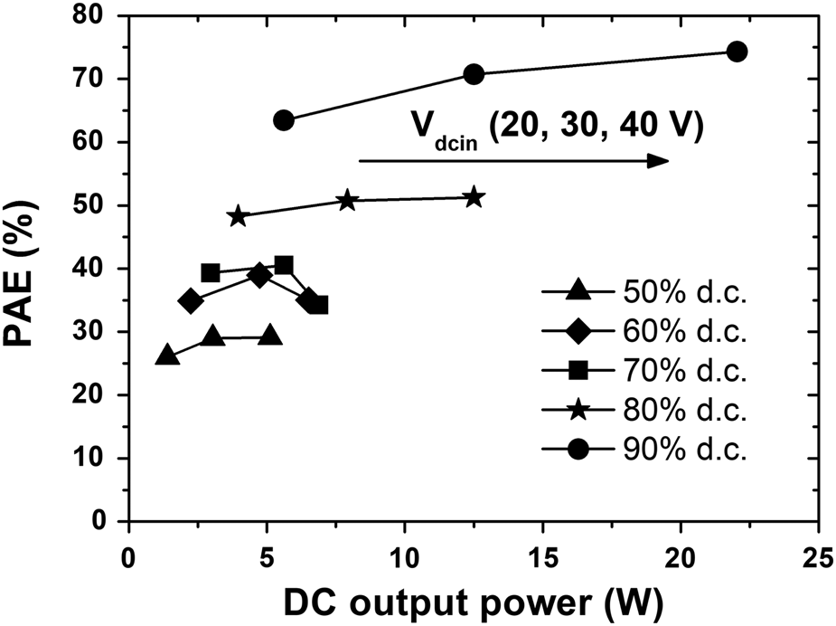
Fig. 7. Measured PAE versus DC output power, DC input voltage (Vdcin) and duty-cycle (d.c.) of the PWM input signal for the realized buck converter module; d.c.: 50 … 90%, Vdcin: 20, 30, 40 V; switching frequency: 1 GHz.
One clearly observes the expected behavior that the efficiency increases with higher duty-cycle peaking at 74% for Vdcin = 40 V and 90% duty-cycle of the PWM input signal. DC output power at a 50 Ohm load reaches 22 W for this condition.
Moreover, for almost every used duty-cycle the PAE rises with DC input voltage at the power stage. In terms of 60 and 70% d.c. one observes a small drop in PAE compared to 30 V supply when operating the converter at 40 Vdcin. In general we have to state that operation for duty-cycles below 50% is very inefficient, i.e., PAE drops down to 20%, when switching the converter at 1 GHz. This is due to the fact that the pulses are getting more narrow (<<1 ns) and thus close to the rise time of the used 2 mm GaN HEMTs in the power stage. Pulses get distorted and the expected output power is not achieved. This will be clarified more in Section “Converter Performance Comparison: 100 MHz versus 1 GHz Switching Frequency.” Here, one has to find the best trade-off between DC output power and speed. But, as this is our first realization, the results are very encouraging for further converter activities.
To have a closer look at the potential of the realized DC/DC converter Fig. 8(a) shows simulated waveforms at input and output while Fig. 8(b) displays measured DC output power (Pdcout) as well as output voltage (Vdcout) and PAE versus duty-cycle for the most challenging conditions, i.e., 40 Vdcin and 1 GHz switching.

Fig. 8. (a) Simulated waveforms of input gate-source voltages Vgs1/2 (RFin1/2–V s in Fig. 1; dotted/solid gray), switch-node output voltage before the filter (RFout in Fig. 1, Vout (dotted black)) and output voltage after the filter (Vdcout; solid black); time section: 30 ns, DC input voltage (Vdcin in Fig. 1): 40 V, switching frequency: 1 GHz, input duty-cycle: 90%. (b) Measured DC output power (Pdcout), DC output voltage (Vdcout) and PAE versus duty-cycle of PWM input signal of the realized buck converter module for power stage supply voltage Vdcin of 40 V and 1 GHz switching frequency.
From Fig. 8(a) one can see the clean switching in the stages of the buck converter in simulations. Unfortunately, correct probing on the chip and at the output before the filter during the measurements was not possible. However, simulations give a good insight. Only some minor distortions due to bond-wires and capacitances of the switching transistors can be observed. The output swing reaches 38 V maximum for a DC input voltage of 40 V. After the conversion circuit (cp. Section “DC/DC Converter Module”) the reached DC voltage is 34 V. This agrees very well with the measured results shown in Fig. 8(b). All three parameters increase when raising the duty-cycle from 50 up to 90%. The DC input voltage of 40 V at the power stage is converted to 33.4 V at the output load (50 Ohm) for 90% d.c. in a 22 W (Pdcout) conversion. With a 50% duty-cycle input signal the PAE peaks at 29% for a 5.1 W conversion to 16.2 V. These efficiency values clearly need improvement and should approach the high duty-cycle ones in further realizations. But as already stated the drop in efficiency for the narrow pulses is an indication for the switching speed limits of the used GaN HEMTs, especially in the final power-stage. There is still room for improvement in further designs. In order to compare with a lower switching frequency the next subsection presents the results for 100 MHz and compares them to 1 GHz.
Converter performance comparison: 100 MHz versus 1 GHz switching frequency
The converted DC output power (Pdcout) and appropriate voltages Vdcout are compared for 100 MHz and 1 GHz switching frequency of the converter, respectively. Table 1 summarizes the results for a DC input supply voltage at the power stage Vdcin of 30 V measured at a 50 Ohm load.
Table 1. Comparison of measured DC output voltage (Vdcout) and power (Pdcout) for varying duty-cycle (d.c.) for realized buck converter module; Vdcin = const. = 30 V

In 100 MHz operation the DC/DC converter delivers for almost every duty-cycle a higher output voltage and thus converted DC output power than for the 1 GHz case. This is a result of the wider pulses arising in the 100 MHz switching case. As already described the pulses get obviously more distorted by the transistors for higher input frequencies due to fT/fmax limits. This will also show up in the efficiency characteristics. They are plotted in Fig. 9 for 30 V DC input voltage and compare the PAE as well as power loop efficiency (ηdrain) for both switching frequencies (100 MHz versus 1 GHz).

Fig. 9. Measured power loop efficiency (ηdrain) and PAE versus duty-cycle of the PWM input signal for 100 MHz and 1 GHz switching frequency of the realized converter; power stage supply voltage (Vdcin) = 30 V.
One clearly observes that the values from Table 1 are translated into the efficiency characteristics of the converter. For all duty-cycles the power loop efficiency in the 100 MHz case stays above 80%, peaking at 87.5% for a d.c. of 90%. Only for the highest duty-cycle tested (90%) the efficiencies for both switching frequencies are converging, i.e., 78% for 1 GHz and 87.5% for 100 MHz. Again, this proves the influence of the frequency limits of the applied GaN HEMTs on the performance.
Another important observation from Fig. 9 is the small difference between PAE and final-stage power loop efficiency of the converter. In the 1 GHz case, the power loop efficiency peaks at 78% while PAE reaches 74% at this point. This proves that the gate drivers of the power stage switches consume very low power which is important for the overall energy budget. Finally, Table 2 compares the achieved results with the state-of-the-art buck converters published working in the hundreds of MHz switching frequency (fsw) region.
Table 2. Comparison of reached converter performance with state-of-the-art GaN-based integrated buck converters

In terms of combining high switching frequencies with high efficiencies and DC output powers beyond 10 W the proposed GaN buck converter module is the best solution to date. If one normalizes the output power values in Table 2 to a total 2 mm final-stage gate-width (far right column) to be comparable we still recognize that the proposed solution represents the best trade-off of all published high frequency converters so far. But as already stated the efficiency drop for duty-cycles below 50% must be solved, also for higher switching frequencies beyond 1 GHz. However, summarizing we can state that the realized GaN-based buck converter module is a suitable candidate for future small and efficient VHF power converters. They can be used for example to replace bulky power supplies for laptops or comparable applications.
Furthermore, it is possible to adapt the fabricated GaN converter MMIC for the modulator part in a broadband ET system. One only has to change the output network. The supply modulator setup is shown and explained in Section “Envelope Tracking Supply Modulator Module” while the measurements will be presented in the following subsection.
Envelope tracking supply modulator characterization
The realized supply modulator has been measured with the same setup described above. A PWM input signal with varying duty-cycle at 1 GHz switching frequency has been applied to the demonstrator. The DC output voltage was measured at a fixed 50 Ω load. Input DC drain supply voltage Vdcin (cp. Fig. 1) was fixed at 27.5 V. This is due to the fact that the targeted main PA (not covered in this paper) requires a drain supply voltage variation between 8… 25 V for optimized efficiencies over a 10 dB power back-off range, which was derived from static measurements. This can be translated into a duty-cycle variation of the PWM input bit stream of the modulator between 30 and 90%, respectively, when assuming a maximum Vdcin at the supply modulator final-stage drain of 27.5 V. Figure 10(a) shows the simulated waveforms at the input and output of the modulator chip (cp. Fig. 1) while Fig. 10(b) plots the measured DC output voltage (Vdcout) versus duty-cycle and the calculated appropriate PAE for the realized ET supply modulator utilizing digital PA approach from Section “Envelope Tracking Supply Modulator Module.”

Fig. 10. (a) Simulated waveforms of input gate-source voltages Vgs 1/2 (RFin1/2–V s in Fig. 1; dotted/solid gray), switch-node output voltage before the filter (RFout in Fig. 1, V out (dotted black)) and output voltage after the filter (Vdcout; solid black); time section: 30 ns, DC input voltage (Vdcin in Fig. 1): 27.5 V, switching frequency: 1 GHz, input duty-cycle: 90%. (b) Measured PAE and DC output voltage (Vdcout) of the realized digital supply modulator circuit for ET applications; f sw = 1 GHz.
The simulated waveforms in Fig. 10(a) show a clean switching of the two stages of the proposed converter MMIC (cp. Fig. 1), which is comparable to the waveforms in Fig. 8(a). Of course, the output voltage after the filter has another shape as, according to the targeted application, a wider passband low-pass filter is used in the ET case. The DC component at the output derived from simulations is 22.7 V which is a bit lower than in the measurements. The results are plotted in the next figure.
From Fig. 10(b), for a switching frequency fsw of 1 GHz, one clearly observes an increase of Vdcout and PAE with increased duty-cycle of the input PWM bit stream. Starting at 8.2 V for 30% duty-cycle the DC output voltage reaches maximum 24.7 V at 90% duty-cycle. This voltage range is sufficient in terms of drain supply for the targeted main RF PA (see above). The appropriate PAE is only 16% for a 30% duty-cycle input signal and peaks at 74% for a duty-cycle of 90%. The efficiency values stay below 50% for duty-cycles up to 60% which clearly needs improvement.
Also, if one would increase the order of the output filter (cp. Section “Envelope Tracking Supply Modulator Module”) we do not expect much higher efficiency values as the insertion losses would increase as well. But a higher suppression of the unwanted frequency components may result in small efficiency increase when conducting modulated measurements in dynamic operation of the ET system. This will be checked in future work with different setups.
But as the focus of this work was primarily on VHF power converters the results are promising, especially against the background of the very high switching frequency compared to other supply modulator solutions so far [Reference Komatsuzaki, Lanfranco, Kolmonen, Piirainen, Tanskanen, Sakata, Ma, Shinjo, Yamanaka and Asbeck4, Reference Hong, Mukai, Gheidi, Shinjo and Asbeck7, Reference Lasser, Duffy, Vance and Popovic11]. However, in fact, for ET systems in the 30 GHz range with targeted modulation bandwidths up to GHz the digital PA approach as a supply modulator is a real alternative but needs a lot of redesign and optimization. This is particularly true for an efficient lower duty-cycle operation in order to not destroy the overall ET system efficiency.
Conclusion
A highly efficient GHz switching GaN buck converter module has been realized and characterized. It includes a compact 2-stage GaN MMIC providing the DC/DC converter circuit with two 2 mm power switch GaN-HEMTs in the final-stage arranged in a half-bridge configuration. Here, no freewheeling diodes to protect the power switches are used which significantly reduces parasitic capacitances and thus improves efficiency. The chip is connected via bond-wires to a hybrid PCB which contains the air-core-inductor based conversion output network. By varying the duty-cycles of the PWM input signal more than 80% power loop conversion efficiency was obtained for output voltages between 13 and 25 V and a switching frequency of 100 MHz. In the 1 GHz switching case the power loop efficiency peaks at 78% for a 22 W conversion to 33.4 V. Here, the power-added efficiency is 74% which proves low gate driver losses in the GaN converter MMIC. The realized module is a good candidate for future GHz-switching small and efficient power converters.
In a second realization the GaN buck converter MMIC has been used with a 700 MHz cut-off low-pass output network to build a supply modulator for future ET systems serving extreme modulation bandwidths in the GHz range. For 1 GHz switching frequency the modulator achieves peak PAE of 74% for 90% duty-cycle PWM input signal. With 30 … 90% duty-cycle variation a drain supply voltage range between 8 and 25 V has been achieved. These two application examples show the flexibility of the digital PA approach.
Acknowledgement
This work was partly funded by the German Federal Ministry of Education and Research (BMBF) under the project reference 16FMD02 (Forschungsfabrik Mikroelektronik Deutschland).
 Andreas Wentzel received the Diploma and the Doctoral degree in electrical engineering from the Technical University of Berlin, Germany, in 2006 and 2011, respectively. Since 2015 he has been the head of the Digital PA Lab in the III-V-Electronics department of the Ferdinand-Braun-Institut, Leibniz-Institut für Höchstfrequenztechnik in Berlin, Germany. His research activities focus on the design, realization, and measurements of flexible digital TX architectures including advanced switch-mode power amplifier concepts realized on GaN and InP from GHz to sub-THz as well as on optimized modulation schemes and filter structures suitable for this type of PAs. Dr. Wentzel is a member of IEEE and MTT society.
 Oliver Hilt received his Ph.D. in Experimental Physics from the Free University Berlin, Germany in 1995 for his work on the charge transport in liquefied rare gases, performed at the Hahn-Meitner-Institut Berlin. He analyzed charge transport in organic conductors and semiconductors for optoelectronic applications at Technical University Delft and University Leiden, both The Netherlands. In 1999 he joined sglux GmbH, Berlin to develop UV photodiodes and promoted to CEO in 2003. Dr. Hilt joined FBH in 2006 for the development of GaN switching transistors for high voltage power applications. He is head of the GaN Power Electronic Devices Lab.
 Joachim Würfl received the Ph.D. degree in electrical engineering from the Technical University of Darmstadt, Germany, in 1989, where he focused on technology and design of high-temperature and high-power GaAs-based devices. As postdoc he developed III/V micromechanical sensors at the same university. Since 1992, he has been with FBH being responsible for clean room technology, process development, and processing of III/V optoelectronic and microwave devices. Additionally, he has been in charge of design and development of power HBTs and power GaN devices. In 2007, he has been appointed Head of business area GaN electronics. In this function, he is managing several projects on GaN-based L- to Ka-band MMICs and high-voltage power switching devices. He is responsible for design, technological implementation, characterization, and reliability testing of these devices. He authors more than hundred scientific papers in related fields. Since 2008 he is additionally acting as CEO of the spin-off company Berlin Microwave Technologies AG (BeMiTec).
 Wolfgang Heinrich received the Diploma, Ph.D., and Habilitation degrees in 1982, 1987, and 1992, respectively, all from the Technical University of Darmstadt, Darmstadt, Germany.
Since 1993, he has been with the Ferdinand-Braun-Institut (FBH) at Berlin, Germany, where he is the Head of the Microwave Department and the Deputy Director of the institute. Since 2008, he has been also Professor with the Technical University of Berlin. He has authored or coauthored more than 350 publications and conference contributions. His present research interests include MMIC design with an emphasis on GaN power amplifiers, mm-wave integrated circuits and packaging, and electromagnetic simulation.
Dr. Heinrich has been serving the microwave community in various functions. He served as Distinguished Microwave Lecturer for the term 2003/2005, as chairman of the German IEEE MTT/AP Chapter from 2002 to 2007, as chair of the MTT-12 Committee on interconnects, packaging, and manufacturing from 2006 through 2008, and as Associate Editor of the IEEE Transactions on MTT from 2008 until 2010. From 2010 through 2018, he was the President of the European Microwave Association (EuMA). He is the recipient of the 2019 EuMA Distinguished Service Award.


