


Introduction
The additive manufacturing technologies now provide extremely fast and convenient technologies for the creation of prototypes dedicated to proofs of concept. They bring an amazing tool for fast evaluation and optimization of microwave components, allowing a shortened time between simulations and actual working devices. These different technologies are now well known by the RF community and have already proven their benefit in different domains of application such as microelectronics [Reference Vaezi, Seitz and Yang1] and filter [Reference Liu, Gong and Chappell2]. Other publications have particularly shown the relevance of 3D printing out of plastic material for antennas [Reference Garcia Lopez, Lopez, Chandra and Johansson3–Reference Bisognin, Titz, Luxey, Jacquemod, Ferrero, Lugara, Bisognin, Pilard, Gianesello, Gloria, Costa, Laporte, Ezzeddine, Lima and Fernandes6] or even tunable filters [Reference Jolly, Tantot, Delhote and Verdeyme7].
It is now possible, due to the great accuracy provided by the present generation of 3D printers, to create prototypes and actual working parts that are high performance [Reference Cai, Khan and Papapolymeou8–Reference von Bieren, de Rijk, Ansermet and Macor13]. Monobloc components are even more desirable since they allow the skipping of the assembly of different parts; the latter option is a great source of annoyance, and field leakage results in poor microwave performance.
Single metallic parts are, of course, a simple solution [Reference Shang, Penchev, Guo, Lancaster, Dimov, Dong, Favre, Billod and de Rijk14–Reference Zhang and Zirath20] to this issue, but single parts made out of metallized plastic are a great intermediate solution as fast and cheap proofs of concept.
In this paper, we propose an extension to a previous work [Reference Sence, Feuray, Périgaud, Tantot, Delhote, Bila, Verdeyme, Pejoine and Gramond21] to use the 3D printing in successive steps (Fig. 1) to create a fast and efficient way to produce 3D printed passive components made out of metal, with plastic materials being only used for early and cheap prototyping. The studied examples are exclusively waveguide components.
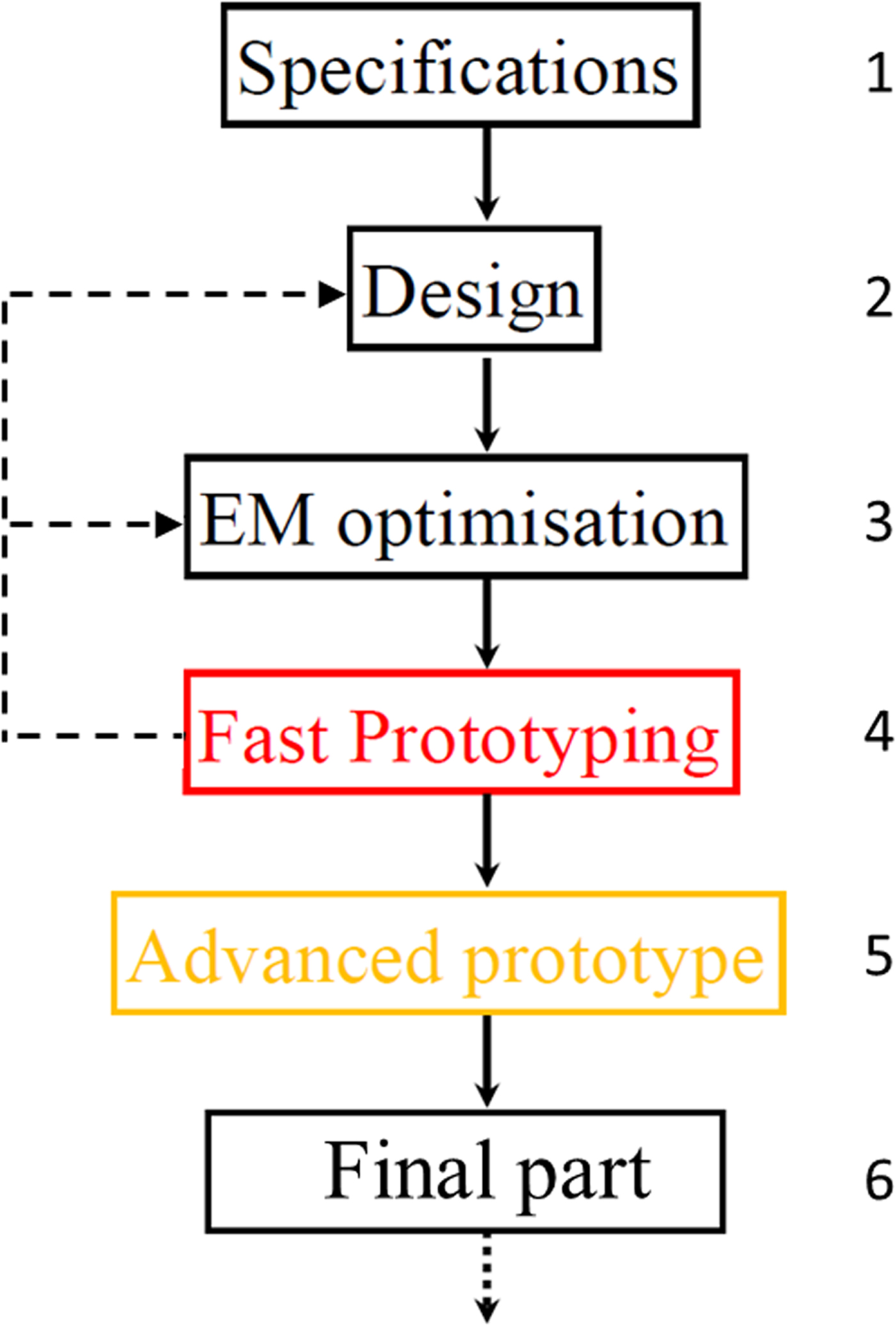
Fig. 1. Prototyping scheme: 3D printed plastic parts as initial proofs of concept before considering advanced and final parts both 3D printed out of metal.
The initial design made in step 2 is done according to the specifications defined in step 1 (Fig. 1). Step 3 is dedicated to the electromagnetic optimization using a full wave simulator (ANSYS HFSS© in our case). The different simulations performed in this paper are made by taking into account the losses coming from the conductive materials (silver coating for the plastic parts, bulk conductivity for the metal parts). Since this information is critical, a dedicated and accurate characterization method must accompany this prototyping scheme and will, therefore, be proposed in this paper.
When the obtained simulated performances are close enough to the initial specifications (step 1), a prototype is made using a fast and low-cost technology, which is, in our case, the plastic 3D printing technology (step 4). This first experimental step is considered to be a companion for the designer to provide valuable experimental feedback and to help obtain the final part by providing early information on the part manufacturing difficulties. If the measured performances of the prototypes (step 4) are not satisfactory, we may return to the optimization step (step 3) and again optimize the component dimensions based on measurements and analysis. If the measured parameters are sufficiently out of agreement with the specifications defined in step 1, we might return to step 2 if we need to define another version of the desired component.
However, this eventuality is not useful if the accuracy of the full wave simulator and printing technology is good enough. The designer can, in this case, directly move to step 5 if the proofs of concept that are obtained in step 4 are sufficiently satisfactory.
Step 4 is thought of as being as quick as possible and the fabrication of monolithic parts is typically the goal to limit the number of manufacturing steps (for example with a minimum number of parts to assemble). Monolithic metallized parts are a desirable goal here, and we can rely on the accuracy of current printers to create tuning-free components. The metallization of the plastic parts must also be as easy, convenient and cheap as possible to enjoy the benefits of this fast prototyping step (step 4).
The plastic printing technology in step 4 must also ideally bring the manufacturing accuracy as close as possible to the technology used in the next step (step 5: advanced prototype).
The optimized CAD file that is obtained in step 4 can, therefore, be used in step 5 with a minimum amount of modification (in some cases even no modifications) or need to re-optimize the component dimensions. Moreover, the real-life device from step 4 gives valuable information regarding the potential difficulties that can arise when moving to step 5 and 6 (advanced and final part, respectively). The component made in this step, even if made with better quality materials (pure metals or alloys), may not be successful after the first fabrication and another fabrication may be needed. Since this part is closer to the actual final part that we are looking for (see step 6), more effort will be placed here to match as closely as possible to the initial specifications (step 1). In other words, step 4 is thought to check the passive components concept and to optimize, with acceptable performance, its dimensions (defining acceptable values for a filter prototype operating frequency and bandwidth for example) but a more meticulous optimization of the component performances will be performed in step 5 (insertion loss, return loss and out of band isolation for a filter, for example) by providing more attention to the tuning of the metal printer parameters.
In our case, the advanced prototype in step 5 will be done with selected laser melting (SLM) technology capable of 3D printing a component directly out of metal. This technology is also more expensive compared with the plastic 3D printing used in step 4. The prototype has good conductivity without any extra steps, compared with the necessary steps in step 4 (low-cost metallization of a plastic part).
Once a prototype in step 5 is considered good enough (metal part from step 5), the final step is triggered, where extra finishing is applied in order to optimize its performance. For example, we typically apply expensive silver plating on the successfully advanced prototype from step 5 to create the final part that matches the specifications defined in step 1.
As an illustration of this prototyping scheme, the first part of this paper will be dedicated to a plastic additive manufacturing technology and, more particularly, to the impact of two manufacturing strategies with the current generation of 3D plastic printers based on the fused deposition modeling (FDM) and polymer jetting technologies. The obtained plastic material complex permittivity will be characterized, as well as its roughness at 10 and 16 GHz. Particular attention will be given to the part surface roughness and manufacturing accuracy for these different strategies. The section ‘Metallization of plastic part’ will then focus on the metallization conductivity of these plastic parts, and a dedicated characterization technique has been developed for that purpose for up to 35 GHz. The proposed method is thoroughly described in this section and applied on low-cost metallization using a paint containing silver nanoparticles.
The section ‘Prototyping of hyperfrequencies filters’ will provide a comparison between two 3D plastic quasi-elliptic bandpass filters made of plastic by the Polyjet © technology and by SLM, the latter filter is being made of stainless steel. Finally, and following the same plastic to metal 3D printing scheme, a last example of the possibility offered by additive manufacturing will be given with a rectangular TE 10 to circular TE 01 mode converter measured from 28 to 36 GHz. A conclusion will summarize the main information in this paper.
3D Printing with plastic material
uPrint SE/Stratasys, Ltd
We first used a machine commercialized by Stratasys. Based on the FDM principle, a layer thickness of 254 µm and a typical accuracy of 200 µm are possible. The FDM technology is based on the extrusion of heated (fused) plastic material: the melted plastic is then printed layer by layer for the creation of the requested 3D parts made most of the time out of ABS (Acrylonitrile Butadiene Styrene) plastic. The ABS plastic is a lightweight and rigid thermoplastic polymer providing good mechanical behavior. Its glass-transition temperature commonly ranges from 105 °C to 115 °C. Different methods have been used for the characterization [Reference Riddle, Baker-Jarvis and Krupka22] of this kind of plastic in the past. Based on the technique described in [Reference Rammal, Tantot, Passerieux, Delhote and Verdeyme23], complementary characterizations have been performed for this paper with the common ABS plastic used with the uPrint SE printer. Its measured characteristics are ε r = 2.55 and tan δ = 3.9 × 10⁻³ at 10 GHz (room temperature). Even if the ABS loss tangent is rather good considering its low cost, the FDM technology quickly reaches its limit in terms of accuracy when applications over the Ku band and above are targeted.
Eden 260 V/Stratasys, Ltd
This other printer can print thinner layers compared with the previous printer. On the high speed (HS) manufacturing configuration, the layers are 33 µm thick and only 16 µm thick when using the high quality (HQ) setup. A typical accuracy ranging from 20 to 80 µm can be observed depending on the manufactured part size. The technology used by this machine is known as Polyjet ©. It consists of the material jetting of photosensitive liquid polymer that turns into solid plastic when exposed to UV light.
Rigid plastic: VeroWhite and VeroClear
Two polymers are commonly available for this printer, the first one being transparent (VeroClear), the second (VeroWhite) being opaque and white. A characterization campaign has been made on these two polymers at 10 and 16 GHz for the HS and HQ printing methods (see Tables 1 and 2). Δ ε r and Δ tan δ represent the errors on the real part of the complex permittivity and of the loss tangent of the characterized plastics respectively.
Table 1. Permittivity of the printed plastics at 10 GHz.

Table 2. Permittivity of the printed plastics at 16 GHz.

The Verowhite and Veroclear plastics clearly show a loss tangent lower than that of ABS, making that kind of plastic not pertinent for the creation of dielectric resonators. We, therefore, determined that the characterized polymers (ABS, Verowhite and Veroclear) make such technologies more interesting to create waveguide components made with metallized plastics walls.
The different printing settings do not create a significant change in the final material properties. However, the accuracy linked to the Polyjet technology is clearly much better than with the FDM process.
Soft elastomer plastic: TangoBlack
Another material, namely, Tangoblack, is commonly available with properties similar to what is observed with elastomers. This rubber-like plastic may be very useful for the junctions of two parts and can be printed with glossy or mat setting. Its characterization has been performed at 10 GHz and the results are displayed in Table 3. Here, the printing settings again do not modify the final part electrical characteristics and this material loss tangent is more than three times higher than with the Verowhite/Veroclear plastics.
Table 3. Permittivity of the printed plastics at 10 GHz.

Manufacturing accuracy
The most direct impact of the printing settings is actually observable on two aspects: dimensional error and mean roughness depth. Focused studies have been performed here based on a close inspection of 50 mm × 50 mm printed plastic substrates. The main results are shown in Tables 4 and 5. The HQ method is clearly more accurate than the HS and produces a smoother surface. Since the Polyjet technique uses a printing head that goes along one specific direction, a clear difference can be observed between the x- and y-axis regarding the accuracy and mean roughness depth. Based on printed 600 µm thick substrates, the typical error on thickness is not modified by the printing method.
Table 4. Manufacturing errors over x-, y-axis and along the z-axis (substrate thickness).

Table 5. Surface roughness over x- and y-axis (Polyjet process).

Metallization of plastic part
Most of the hyperfrequency applications will need to rely on metal enclosure (shielding, ground plane, etc.) at some point. Even if many examples of 3D dielectric parts metallization can be found in the literature [Reference Lohinetong, Minard, Nicolas, Le Bras, Louzir, Thevenard, Coupez and Person24–Reference Tsang, Gu and Braunisch26], the use of silver paints provided by Ferro is preferred here for its simplicity, ease of application and cost. The only constraint is that curing is needed after deposition of this coating. This is applied on plastic parts (Polyjet technology) that allow curing up to 40 °C. This temperature is 23% lower than the plastic materials temperature of glass-transition. One, two, and three successive layers (each layer is cured before applying the next layer) of this silver paint have been applied for the measurement of their conductivity at 10 GHz and 35 GHz with a nondestructive method based on the resonant cavity.
A cylindrical cavity can be used with the TE 01p resonance mode, which is less sensitive to the contact default. The top cover of this cavity is replaced by the metal surface to be characterized (Fig. 2). The measurement of the unloaded quality factor, which is proportional to the root of conductivity, can lead to unknown conductivity due to a simple analytical EM model.
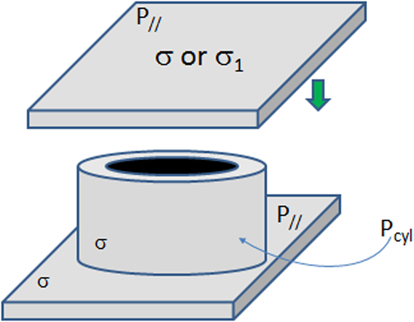
Fig. 2. Drawing of the mixed conductivity cavity on TE 01p mode.
For the TE 01p mode, there is only one component of the electrical field E φ [Reference Boudouris27] and two components for the magnetic field H r and H z, where none of these components are dependent on the variable, φ and the other field components are zero.
With the electromagnetic field equations given by [Reference Boudouris27], the unloaded quality factor (1) can be calculated from the calculation of metallic losses (2), and the energy stored in the volume of the cavity (4).
 $$Q_0 = \omega \displaystyle{{E_T \,_{}} \over {P_m \,_{}}},$$
where E T is the total EM energy stored in the circular cavity.
 $$P_m = \displaystyle{{R_s} \over 2}\int\!\!\int {\vec H\vec H^ * \,d\vec S},$$
where R s is the surface impedance,
 $$R_S = \displaystyle{1 \over {\sigma \delta _S}} = \displaystyle{1 \over {\sigma \sqrt {2/\mu _0 \mu _S \omega \sigma}}} \;{\rm and}\;\mu _S = 1,$$
 $$E_{T} = \displaystyle{1 \over 2}\int\!\!\int\!\!\int {\varepsilon _0 \varepsilon EE^ *} dv.$$
For the metallic losses of the cavity that depend on the surface impedance (equation 2):
 $$P_{m} = P_{cyl} + P_{//\sigma 1} + P_{//\sigma \,},$$
where P cyl represents metallic losses on the cylindrical wall, P //σ1 represents the losses on the parallel wall with the conductivity σ 1, and P //σ is the term identical to P //σ1 for the bottom wall with the conductivity σ.
Using equation (2), we calculated the expression of losses for each part of the cavity, either P //σ for the top and bottom covers, or P cyl for the circular surface.
Thus, after calculations, we can have the unloaded quality factor Q 0mix of the cavity (mode TE011) when the unknown metallized plate (unknown conductivity σ 1) is on the top of the cavity, it can be expressed as follows:
 $$Q_{0mix} = \displaystyle{{\pi f_0 \mu _0 H_c R_c} \over {R_{s1} (k_g^2 /k^2 )R_c + R_s \left( {(k_g^2 /k^2 )R_c + (k_c^2 k^2 )H_c} \right)}},$$
with k = 2π/λ, k g = π/H c, and k c = x′01/R c
where: λ is the wavelength, x′01 is the first zero of J′0(x), is the derivative of the first kind of the Bessel function order, R c is the radius of the cavity, H c is the height of the cavity.
For different dimensions of a cylindrical cavity on the TE 01p with different conductivities, analytical calculations were validated by comparing the obtained Q factor with full-wave simulation software (HFSS).
After calculations, we obtained the expression of the conductivity in terms of the cavity dimensions and of the measured unloaded quality factor Q 0mes.
 $$\sigma = Q_{0mes}^2 \,\displaystyle{{\left( {2(k_g^2 /k^2 )R_c + (k_c^2 /k^2 )H_c} \right)^2} \over {\pi. f_0 \mu _0 H_c^2 R_c^2}} = \displaystyle{{Q_{0mes}^2} \over {K_t^2}}.$$
In the same way, the expression of the unknown conductivity σ 1 that we intend to characterize, with the measurement of the unloaded quality factor Q 0mix, is
 $$\eqalign{\sigma _1 &= \cr & \displaystyle{1 \over {{\left( {(H_c/Q_{0mix})(\sqrt {\pi .f_0\mu _0} /(k_g^2 /k^2)) - (1 + (k_c^2 H_c/k_g^2 R_c))(1/\sqrt \sigma )} \right)}^2}}.} $$
The uncertainty on the unloaded quality factor is calculated using the expression of the measured loaded quality factor Q L mes, of the uncertainty of the resonance frequency and of the module of the transmission coefficient at f 0:
 $$\eqalign{\Delta Q_{0mes} =& \left( {\displaystyle{{\Delta f_0} \over {\,f_0}} Q_{L\;mes} + \displaystyle{{2Q_{L\;mes}^2 \Delta f_1} \over {\,f_0}}} \right)\displaystyle{1 \over {1 - \left \vert {S_{21}} \right \vert _0}} \cr &+ \displaystyle{{Q_{L\;mes} \Delta \left \vert {S_{21}} \right \vert _0} \over {(1 - \left \vert {S_{21}} \right \vert _0 )^2}},}$$
where f 0 is the resonant frequency of the selected mode, f 1 and f 2 are the frequencies at −3 dB of |S 21|@f 0 dB, Δf 0 is the uncertainty on f 0, Δf 1 = Δf 2 is the uncertainty on f 1 or f 2.
The uncertainty on the conductivity can be expressed as
 $$\Delta \sigma = \displaystyle{{2Q_{0mes} \Delta Q_{0mes}} \over {K_t^2}},$$
where K t is a form factor given in (7), and Δf 0 has been neglected.
In expression (10), the uncertainty brought by the dispersion of the inner dimensions of the cavity is neglected due to an accurate determination of the height and diameter from the resonant frequency expressions of the first two modes TE011 and TE012.
To calculate the uncertainty on σ 1, partial differential equations were performed, taking into account the uncertainties ΔQ 0, Δf 0, and Δσ.
The greatest cause of uncertainty on the Q factor comes from the TE 011 mode power coupling to the degenerate TM 111 mode which requires a quarter-wave post to remove it.
Considering that the larger the diameter of the cavity is, the lower the characterization uncertainty, we have increased the diameter of the cavity by limiting it to the usual lateral dimensions used for dielectric substrate characterization methods (based on resonant cavities) at these frequencies.
The diameter of the cavity was thus set to Øc = 50 mm and h = 21.98 mm to conserve a 10 GHz resonance frequency of the TE 011 mode. For the 35 GHz cavity, these dimensions were set to Øc = 12.4 mm and H c = 7.6 mm (Fig. 3). Different measurements were performed with these cavities.

Fig. 3. Copper cavities at 10 (left) and 35 GHz (right).
First, we have measured the conductivity of the first cavity designed to operate at 10 GHz and made with high-grade copper. An average value of σ = 51.5 ± 0.9 S/μm (±1.7%) was obtained for ten measurements. These results confirm the potential of the cavity for measuring the conductivity of conductive material having a planar surface. Another cavity operating at 35 GHz cavity and manufactured in a lower quality copper has an equivalent conductivity of σ = 41 ± 0.8 S/μm (±2%). These two cavities will then be used to measure the unknown conductivity σ 1 of different metals by replacing their top wall with the metal to be characterized.
A series of measurements have been conducted for different full metal plates (copper, aluminum, and brass plates) without surface finish and copper laminated FR4 substrates. The retrieved values are reproducible with well-mastered uncertainties. The values are consistent with the literature.
The good repeatability of the measurements is linked to an adequate Ø/h ratio and to the adding of a quarter-wave slot in the lower part of the cavity that allows the removal of the TM 111 resonant mode, which is degenerated. Without such a slot, the obtained results have unacceptable errors because the TM 111 can easily be excited for metal plates with irregularities on their surfaces.
As a next step, uncertainties of the measurement of the Q factor can be improved by the use of the complex response of the transmission parameter [Reference Kajfez28, Reference Bartley and Begley29] to extract the quality factor.
This procedure at 10 GHz has also been applied on VeroWhite and VeroClear plastics printed by the Polyjet technology and the measured results are displayed in Fig. 4. The number of layers of this silver paint clearly impacts the obtained conductivity. After three layers, the conductivity remains approximately 1.65 S/μm without observing a clear impact of the initial surface roughness. Because the metal paint is applied by hand, the thickness of a single layer is not perfectly reproducible and has been measured between 5 and 7 µm.

Fig. 4. Measured conductivity (S/µm) at 10 GHz of the silver paint over plastic parts.
Figure 5 shows the measured conductivity of the silver-painted plastic plates (three layers of silver paint) at 35 GHz. Apart from the Verowhite HQ case, which shows a conductivity of 0.71 S/μm, the other measured conductivities remain under 0.2 S/μm at 40 GHz. We then conclude that the roughness of the plastic part (ranging from 4.4 to 10.9 µm) is creating a large drop for the conductivity as the frequency increases from 10 to 40 GHz.
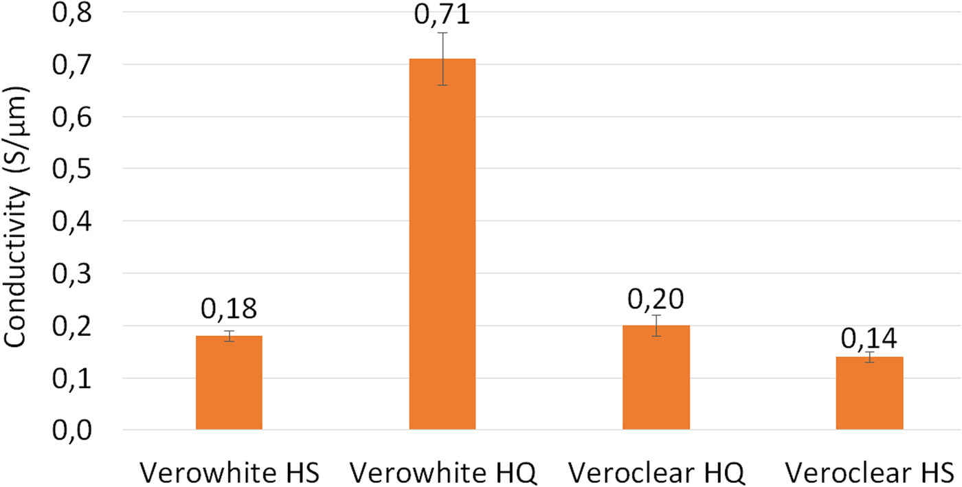
Fig. 5. Measured conductivity at 35 GHz of the silver paint over plastic parts (3 layers of silver paint).
Prototyping of hyperfrequencies filters
To evaluate the potential of these two plastic printing technologies (and the coating procedure) for the creation of microwave components, two bandpass filters have been designed. Because of the rather low accuracy of the FDM process, a first 4 poles 2 transmission zeros filter is designed approximately 6 GHz. The second one uses the exact same topology; however, it is designed approximately 12 GHz by applying a scaling factor on the previous component and a re-optimization step, considering that the Polyjet technology used for this case can provide enough accuracy for this frequency range. The filters are first synthetized based on initial specifications, and a theoretical coupling matrix is defined accordingly. Then, the full wave simulator is used to perform an optimization of the filter geometrical parameters. The extracted coupling matrix coming from the simulator optimization steps are compared with the ideal matrix, and the parameters are refined until the extracted coupling parameters are close enough to the ideal ones.
A comparison will also be made with a similar filter made with SLM technology out of stainless steel (AISI 316L). An AM250 metal printer from Renishaw is used here by our partner [Reference Bartley and Begley29]. This technology uses a laser to melt a powder bed, making the fabrication of layer-by-layer 3D part possible. The available metals are typically stainless steel, titanium, and aluminum alloys. The manufacturing tolerance is directly linked to the laser diameter and is close to 100 µm in this study. Since this accuracy is close the Polyjet© technology accuracy, the CAD files from step 4 (see Fig. 1) can be used in step 5 with this technology with very few modifications. The machine build volume is 250 × 250 × 300 mm3. The thickness of the manufactured layers is directly linked to the powder diameter (tens of μm).
Figure 6 shows the two different plastic filters made for this purpose. Because the obtained results (Figs 7 and 8) were good enough with the first and only fabrication, no extra EM optimization (in other words, moving back to step 3 in Fig. 1) was performed. The 6-GHz filter made by the FDM technology was constructed from ABS material and is 99 × 118 × 81 mm3. Because of its size, it has been made in three different parts in order to make the painting step with the silver paint easier. Cutting planes along the E-plane were chosen in order to minimize leakages. Three layers have been applied and cured. Then, the silver-coated parts were assembled with screws and bolts. Since flanges are made within the part, the filter was then ready to be measured. The 12-GHz filter measures 46.5 × 55 × 38 mm3.
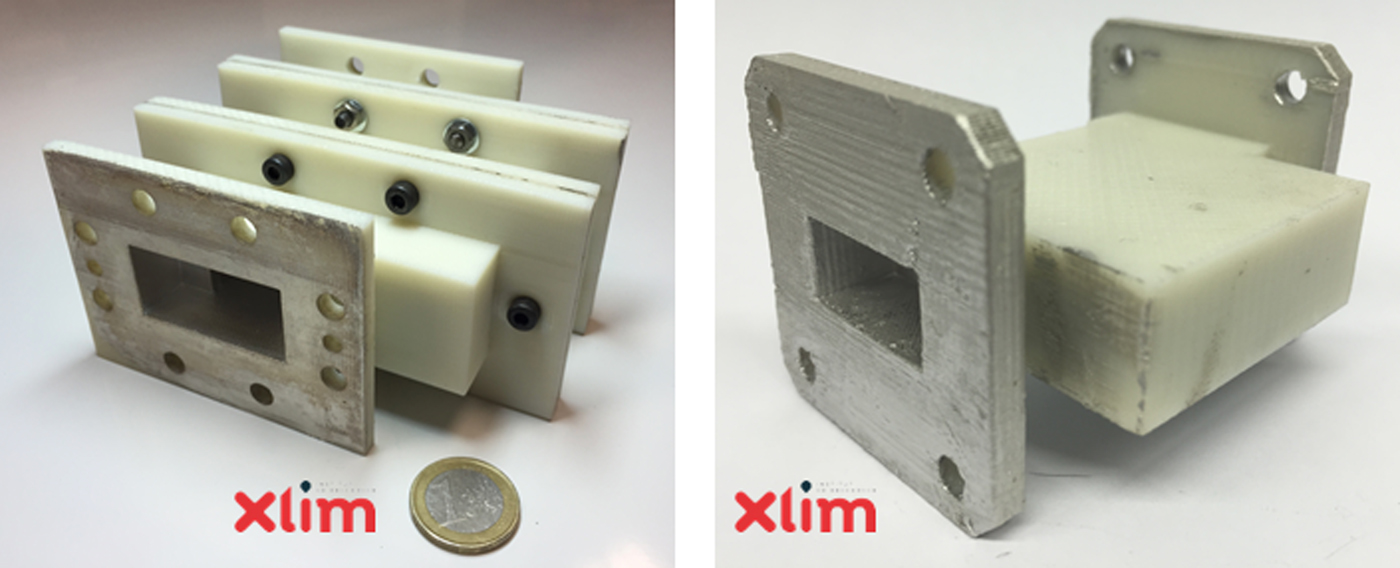
Fig. 6. (left) Bandpass filter made by the FDM technology and working at 6 GHz, (right) bandpass filter made by the Polyjet technology and working at 12 GHz.
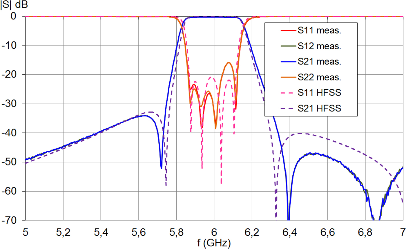
Fig. 7. Simulated and measured S parameters of the ABS filter made by the FDM technology.
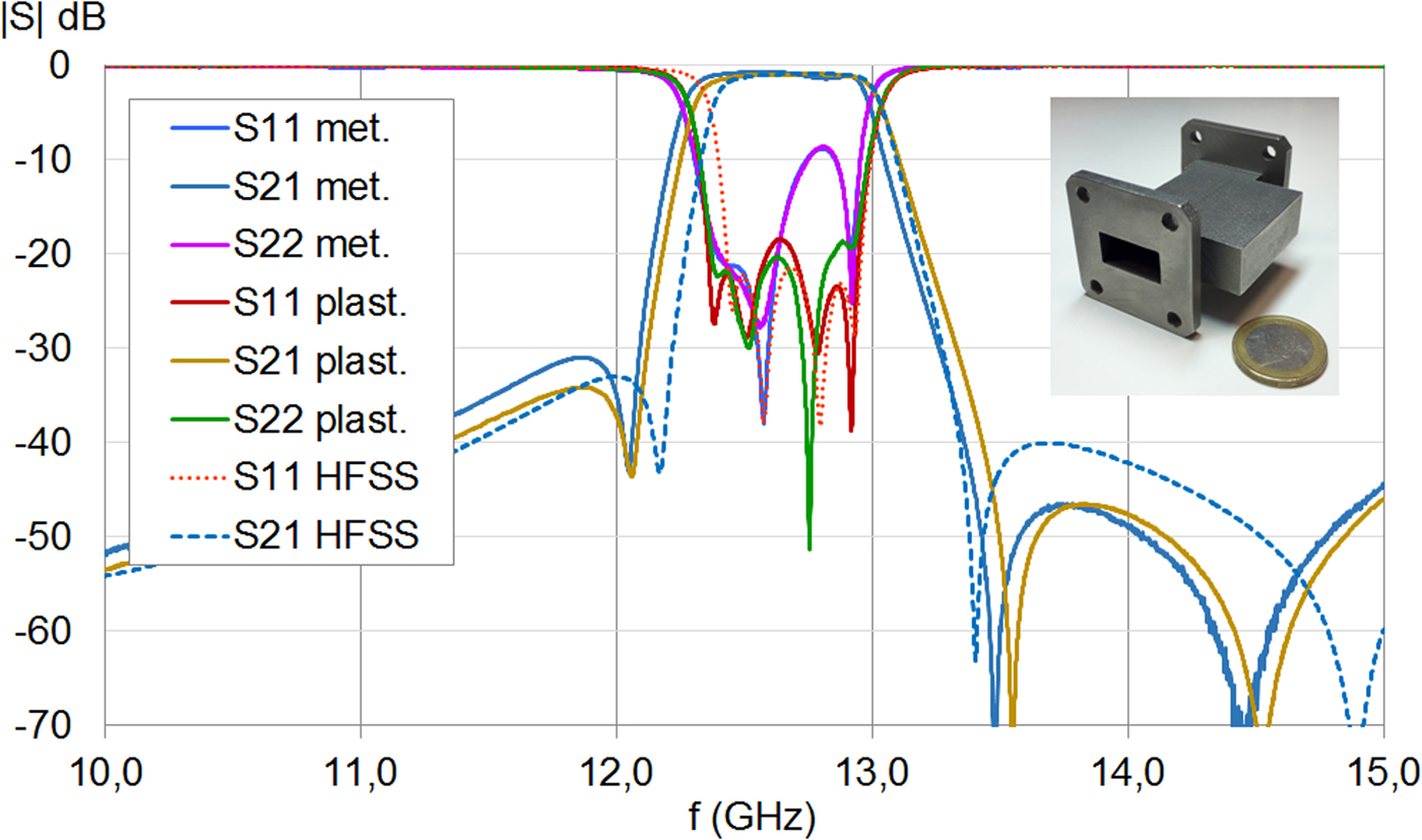
Fig. 8. Measured and simulated S parameters of the filters (plastic and metal); stainless-steel filter made by SLM is also displayed.
Figure 7 shows the simulated and measured results for the 6-GHz FDM filter, confirming a very good behavior. It should be noted that no tuning screws were used here.
The smaller prototype (shown in Fig. 6), designed to work approximately 12 GHz, was made within just one part using the Polyjet technology. For its metallization, the Ferro silver paint is simply poured into the filter. The exact replica of this filter has also been made out of stainless steel and is shown in Fig. 8. The additively manufactured filters are perfectly measurable with S parameters very close to the expected behavior (Fig. 8), especially in terms of central frequency.
The first row of Table 6 shows the simulated results of the filter considering a conductivity of 1.65 S/μm (see Fig. 4). The middle row summarizes the measured results of the Polyjet filter metallized with the silver paint. Extra calculations show that an equivalent conductivity of 0.3 S/μm can explain the higher measured loss. We suspect that the inner faces of the filter, hardly accessible during the removing of the filter inner support with a high-pressure water jet, may be rougher than that measured with simple plates (Table 5). Moreover, since the paint was simply poured into the Polyjet filter, no control was performed on the quality of the successively applied metallization layers. Even if this value is really low, it is sufficient to validate the plastic prototype in step 4 and move to step 5 (Fig. 1). The measured IL of the stainless-steel filter, which is the advanced prototype filter of this study, is 0.66 dB. We can assume that the low conductivity of the stainless-steel material (1.1 S/μm considering the stainless-steel bulk conductivity) and the fact that the SLM creates quite rough lateral walls inside the filter are responsible for such losses. We have evaluated the inner walls conductivity to be approximately 0.35 S/μm. Even if this value is exceptionally low, it is sufficient to validate the prototypes in step 4 and move to step 5 (Fig. 1).
Table 6. Characteristics of the 12 GHz filters.

The estimated Q of the resonators with the silver-painted plastic filter and stainless-steel filter are respectively approximately 450 and 600 at 12.7 GHz. For that measurement and compared to [Reference Sence, Feuray, Périgaud, Tantot, Delhote, Bila, Verdeyme, Pejoine and Gramond21], the filters flanges have been milled in order to get a better contact with the waveguide connectors used with our VNA.
The part produced from metal, shown in Fig. 8, is the first and only advanced prototype of step 5 (see Fig. 1) showing a return loss of 8.6 dB. This value is lower than that achieved with the plastic part due to the non-optimal manufacturing from the SLM process. A deeper analysis of the filter's inner dimensions by a destructive approach would be needed to optimize the metal printer fabrication parameters in order to obtain a better accuracy and move with confidence to the final part.
Mode converter
The mode converter [Reference Schulz, Rolfes and Will30–Reference Smith and Mongold33] is a typical device that needs a very complex shape requiring very specific manufacturing technology (electroforming traditionally). It, therefore, requires a highly skilled manufacturer and a very high manufacturing time, and it costs a lot of money. Additive manufacturing brings with this highly demanding application a very beneficial improvement. The main challenges of this type of devices are to provide the highest modal purity, a useful bandwidth that is as wide as possible and the lowest possible insertion loss. The last component proposed in this paper is the optimization of an initial design proposed in 1958 by G.R.P. Marie [Reference Marie32] (Fig. 9). The full wave simulator is used to make a parametrical optimization of the geometrical key parameters i.e., the dimensions of the different wave guiding sections.
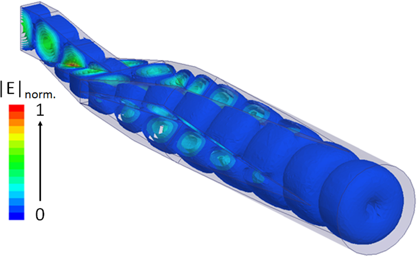
Fig. 9. E field in the mode converter of G.R.P. Marie.
The TE 10 rectangular waveguide mode is converted to the TE 20 mode of a larger rectangular waveguide to maintain the same operating frequency band. This rectangular waveguide is split at the ends to form a cruciform structure that can be considered to consist of four rectangular waveguides with an electric field mimicking the TE 10 mode. Finally, the slots of this cruciform guide are reduced to transform it into a circular waveguide where the TE 01 mode can propagate (Fig. 10). The optimization process on HFSS has been more specifically conducted on every section of the converter with a target return loss of 45 dB from WR TE 10 to circular spurious modes and 30 dB for the TE 01 for 6.5–32.5 GHz frequency band. All parts have been assembled and optimized with the same previous objectives.
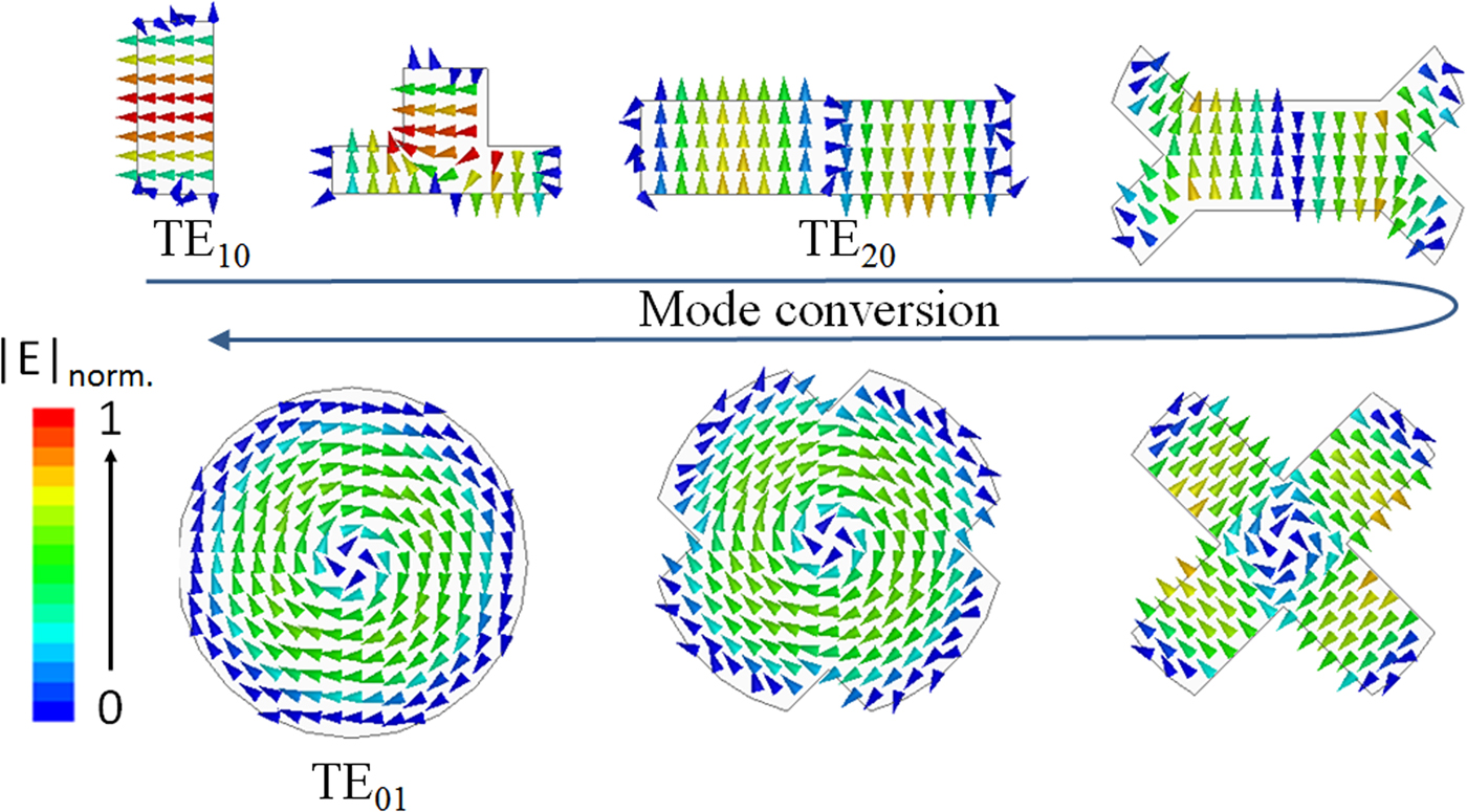
Fig. 10. Mode conversion for the electric field in different steps of the transition.
The transmission coefficient of the two cross-polarized fundamental modes in the circular waveguide (TE 11// and TE 11⊥), the two cross-polarized modes TE 21// and ⊥, the TM 01 mode and the fundamental TE 10 of the rectangular waveguide are less than −40 dB for the entire frequency range. The degenerate mode TM 11 transmission coefficient is less than −25 dB.
The rectangular waveguide operates in the Ka band (WR28), and the diameter of the circular waveguide is set to 14.2 mm for a cut of the frequency of the TE 01 mode equal to 25.6 GHz. The total length of the structure is equal to 94 mm.
This rectangular TE 10 mode to circular TE 01 mode converter has been made out of plastic and stainless steel using the same technologies as in the previous part (Fig. 11) and within just one part. The parts presented here have only been made once; no extra manufacturing or EM optimization steps were performed. The two manufactured mode converters have been assembled in a back-to-back configuration and the obtained S 21 parameters (WR TE 10 towards WR TE 10) have been measured (Fig. 12). Figure 13 presents the measurements of their S 11 parameters. The results show a particularly good agreement between simulations and experimental results for the metal part. The silver paint used for the plastic metallization brings too large of a metallic loss, and the poor quality of the plating on the internal sharp edges of the converter causes small resonances in the structure. This latter point has been confirmed by full-wave simulations. However, since the SLM technology will solve this problem, step 4 is considered sufficient (proof of concept working on the expected frequency band with the expected modal purity) to move to step 5. Combining the plastic and metal parts confirms that the high insertion loss, in that case, is due to the plastic part metallization that is less performant compared with the stainless-steel part. Looking at the used metal (silver paint, stainless steel) conductivities, the plastic part should have better performances if the paint would be more uniformly applied. However, since we have a very limited control of the plastic part inner metallization, the metal part presents lower IL even if its conductivity is lower to what can be obtained from the silver paint if a perfect coating is reached.
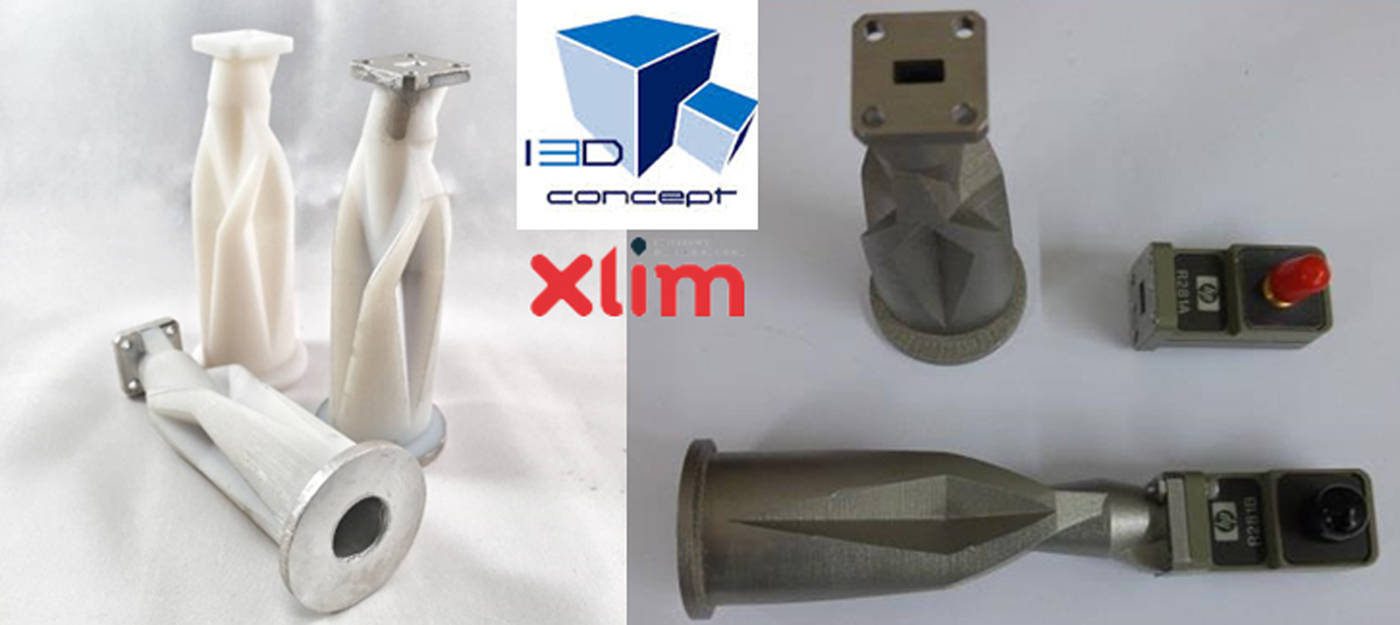
Fig. 11. Manufactured mode converter made out of plastic (left) and stainless steel (right) before measurement.

Fig. 12. Measured and simulated S 21 for a direct connection metal assembly.

Fig. 13. Measured and simulated S 11 for direct connection assembly.
Within a back to back configuration, the second mode converter is placed at three different angles (0°, 45°, and 90°) and the corresponding S parameters are measured for each case. Figure 14 shows excellent results during this operation, thus confirming the simulated good robustness towards rotation.
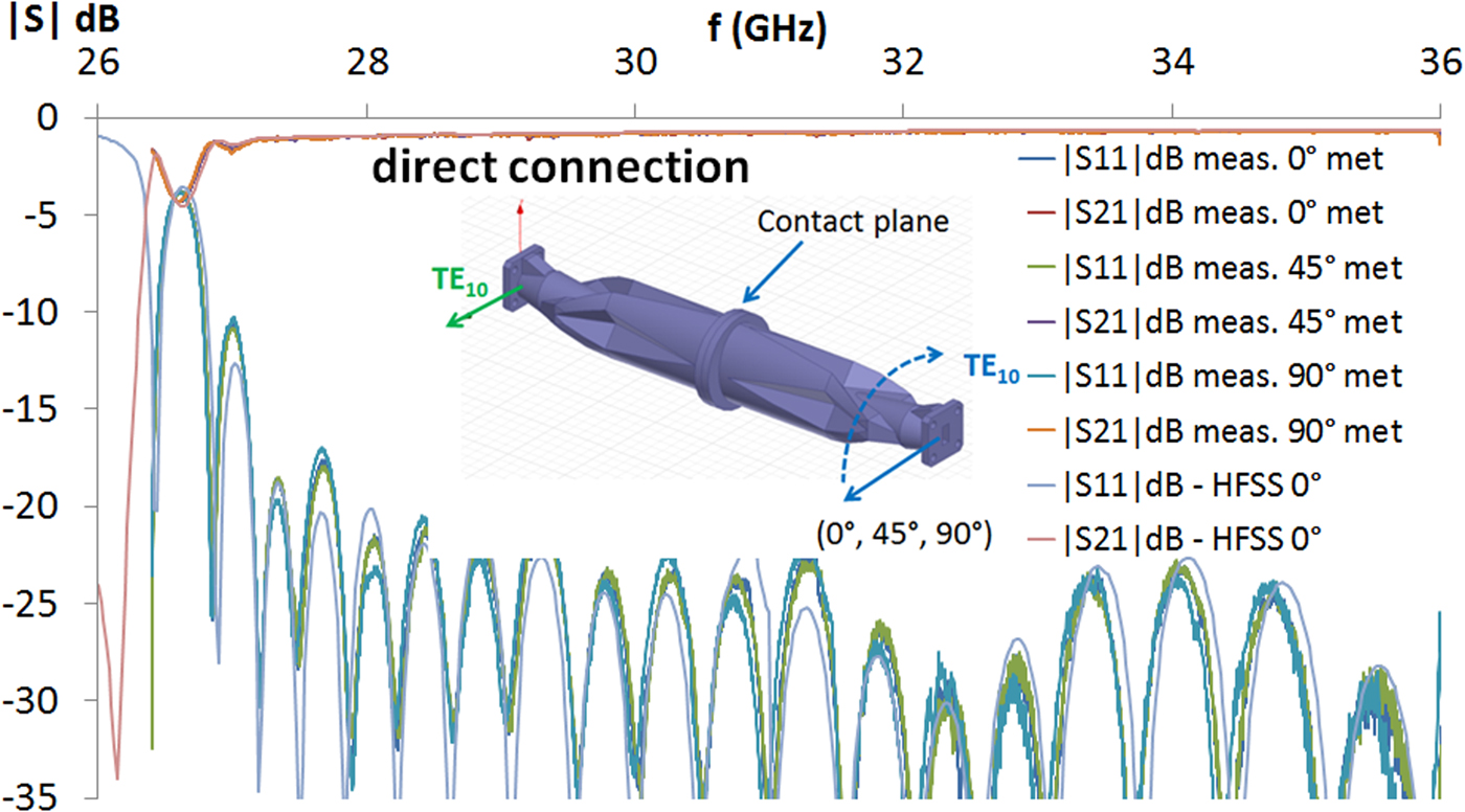
Fig. 14. Measured and simulated S 21 for a direct connection with rotation alignment.
The measured results confirm a very high agreement with the simulated curves when considering an equivalent conductivity of the stainless steel of approximately 0.82 S/μm (1.1 S/μm in theory). Conversions into other modes (TE 11, TM 01, TE 21) are suppressed by more than 45 dB. The typical insertion loss remains between 0.6 and 0.95 dB from 28 GHz to 36 GHz. Compared with [Reference Schulz, Rolfes and Will30], the obtained results show better insertion loss, a higher relative bandpass (25%), and finally a working device in the Ka band that does not need any assembly of different parts nor tuning elements.
Conclusion
This paper gives an overview of the potential of plastic and metal additive manufacturing with the FDM, material jetting (Polyjet ©) and SLM technologies. The properties of different plastics commonly used with plastic printers have been characterized up to 16 GHz, and the ABS showed a better loss tangent (3.9 × 10⁻³) than the plastic used with the Polyjet technology (2 × 10⁻²), even if it remains too lossy to create resonant components. The manufacturing methodologies (HS or HQ) show a very limited impact on their complex permittivity, the accuracy and surface roughness, which are the most impacted parameters for a printed part. A silver plating technique of such plastic parts has been studied, showing that a minimum number of three layers are needed. Even if low curing temperatures of this paint should be used (40–80 °C depending on the used plastic), a typical conductivity of approximately 1.65 S/μm at 10 GHz has been measured thanks to a simple but accurate characterization method based on a resonant cavity. Even if this value quickly drops in frequency (0.2 S/μm at 35 GHz), this plating method is suitable for prototyping microwave components as demonstrated with the proposed quasi-elliptic bandpass filters working at 6 and 12 GHz and the Ka band mode converter. These components, and especially the components made in a single part, have proven their capability to make low cost and efficient proofs of concept for passive hardware. Because of the frequency ranges that are considered in this paper and the combined accuracy of the plastic printers and full wave simulators, there was no need to re-optimize the obtained plastic prototypes. The fabricated plastic parts, which are presented in this paper, have indeed only been made once. These plastic prototypes appear, from our experience, to be very valuable and low-cost real-life parts that will help in identifying the manufacturing challenges of the advanced and final parts, rather than an intermediate object that requires extra electromagnetic optimization since it was not needed at all.
More performants components can, after that step, be considered using advanced technology as it has been done with the SLM technology. This next step has been applied to create a monolithic bandpass filter and rectangular TE 10 mode to circular TE 01 mode converters, which provide better performance. The mode converter with its complex geometry and single part fabrication appears to be an excellent example of the potential of the additive manufacturing for microwave components. This example more particularly shows excellent agreement with theoretical simulations, state of the art performances within a monolithic configuration and without any tuning devices.
 Johann Sence was born in Châteauroux, France in April 1987. He received the iXeo high-technology engineering Master degree with an excellence grant from the University of Limoges, Limoges, France. He is currently finishing his Ph.D. at XLIM, University of Limoges, with the support of a partnership between the French National Research Agency (ANR) and the French Defense (DGA). His research activities focus on the co-design and the co-integration of RF front-end systems.
 William Feuray was born in 1988 at Bordeaux (France). He did all his years of University at Limoges (France) and received B.S. (2012) and M.S. degrees (2014) in electrical engineering. After that, he received the Ph.D. degree from the University of Limoges, France in 2017. The subject of his thesis was on tunable multiplexers for space application and he worked in collaboration with the French National Space Studies Center (Toulouse, France) and the Thales Alenia Space Company (Toulouse, France).
 Aurélien Périgaud was born in Limoges, France, in 1981. He received the Ph.D. degree from the XLIM research institute, University of Limoges, Limoges, France, in 2009. He is currently a Research Engineer at XLIM, University of Limoges. His research activities are mainly dedicated to the packaging of millimeter-wave modules and to the design and optimization of original resonators and filters.
 Olivier Tantot (51 years old) received his Ph.D. degree in electronics in 1994 from the University of Limoges, France. Since 1994, he has been a researcher at the “Institut de Recherche en Communications Optiques et Microondes”, Limoges. Since 1997, he is an associate professor at XLIM Laboratory of Limoges (France) and he works on new methods of material characterization for thin films or bulk materials at low and high frequencies. He also has an interest in microwave tunable filters for space applications and additive manufacturing for RF components.
 Nicolas Delhote (36 years old) received his Ph.D. degree in 2007 from the XLIM research institute and has then joined XLIM since that date. He is specialized in 3D manufacturing technologies for the fabrication of RF and millimeter waves passive components (filters, waveguides, RF transitions, etc.). He has more particularly focused most of his activity on additive manufacturing technologies for high-end applications (space telecommunications, airborne radar applications, high frequency wireless telecommunications). Since 2016 he is the head of the MACAO team (eight faculty members, 12 Ph.D. students, and postdoc).
 Stéphane Bila (M'10) was born in Paris, France, in September 1973. In 1999, he received the Ph.D. degree from the University of Limoges, Limoges, France. In 2000, he became a researcher CNRS and joined XLIM, Limoges, France. From 2006 to 2015, he led a research team focused on passive microwave circuits, and since 2016, he leads the RF Systems department working on microwave circuits, antennas, and EMC. In 2012, he became a scientific representative for the CNRS with expertise in the field of antennas and microwave systems. He was in the Editorial Board of the International Journal of RF and Microwave Computer Aided Engineering, in 2014 and 2015, and since 2016, he is an Associate Editor of the IEEE Transactions on Microwave Theory and Techniques. His research activities concern computer-aided techniques for the advanced design of microwave circuits, including filter synthesis, numerical modeling, and optimization techniques.
 Serge Verdeyme was born in Meilhards, France, in June 1963. He is currently a professor at the University of Limoges, France. He develops his research activities in XLIM laboratory, in the field of numerical modeling, optimization of microwave components and circuits, with a particular experience in the design of microwave filters and multiplexers. He has been the supervisor of the thesis of 39 Ph.D. students, he co-authored four book chapters and 73 international refereed journals, and more than 150 International conference papers. He is vice-president of the University of Limoges since 2010.
 Jean-Baptiste Pejoine received his engineering degree from the Ecole Nationale d'Ingénieurs de Tarbes in 2011. Thanks to his multidisciplinary profile, he joined a major French automotive group and other SMEs where he was a project manager dedicated to prototyping for the automotive industry. He then started in 2015 a SME called I3DConcept which is specialized in the additive manufacturing of metal parts for various industrial applications.
 René-Philippe Gramond was born in 1961. He is currently a certified professor (professeur certifié) in mechanical engineering in the Turgot High-school in Limoges, France. His activities are focused, among others, on additive manufacturing applied to the fast prototyping of advanced components for various applications.


