INTRODUCTION
Large capacitive energy storage systems are being implemented for powerful laser systems (Miller et al., Reference Miller, Moses and Wuest2004; Cavallier et al., Reference Cavailler and Fleurot2004), electromagnetic launchers (Hundertmark et al., Reference Hundertmark, Schneider and Vincent2013; Hsu et al., Reference Hsu, Merritt, Moser, Awe and Brockington2012), and pulsed high magnetic field facilities (Zherlitsyn et al., Reference Zherlitsyn, Wustmann, Herrmannsdörfer and Wosnitza2012; Sims et al., Reference Sims, Rickel, Swenson, Schillig, Ellis and Ammerman2008). The most famous giant Nd:glass laser, which has been in operation since 2010, is the Lawrence Livermore National Ignition Facility (NIF, 192 × 2.2 MJ capacitive modules; Hinkel et al., Reference Hinkel2013). The second one is the Laser Megajoule Facility, which is being constructed by the Commissariat a` l`Energie Atomique (LMJ, 480 × 0.86 MJ capacitive modules; Ebrardt & Chaput, Reference Ebrardt and Chaput2010).
Powerful electromagnetic launchers, such as US Navy project (55 × 3 MJ + 28 × 1.3 MJ capacitive modules; McNab et al., Reference McNab, Fish and Stefani2001), are also based on modular capacitive storages. Basic requirements for modular capacitive storages for large laser systems were introduced while developing large facilities such as the Shiva family (up to 20 MJ stored; Kemp et al., Reference Kemp1976) and Nova with 60 MJ (Witham et al., Reference Witham, Merritt, Holloway, Gritton and Oicles1981). High voltage, high current pulse shaping inductor, which is able to withstand high action integral, is one of the critical components of a power conditioning system. The inductor should tolerate very intense mechanical and thermal shocks imposed by high peak current, and provide long service life. Large number of modules imposes strict requirements on the parameters of a pulse shaping inductor. These include reliability, cost minimization, ability to withstand failure regime, stability from shot to shot in controlled parameters, limits on size and weight, easy maintenance, long lifetime (ideally full duty time of a capacitor bank), and environmental safety.
The protection inductor should also have low stray electromagnetic fields and low resistance. The stray field interferes with other electronic elements of the power supply. Lower stray field can reduce the distance between the inductor and other elements, and therefore the volume of the power supply can be reduced. The resistance of the inductor dissipates energy during the discharge and therefore decreases the efficiency of a power supply system.
A 25 kV/40 kA protection inductor on 1 mH has been investigated recently (Lv et al., Reference Lv, Qiu, Zhang, Tang and Li2010a; Reference Lv, Qiu, Tang and Li2010b). The main disadvantage for this inductor is winding by wide 4 × 45 mm2 strip, which is definitely not technological, and the use of outer stainless steel ring for the coil embedment and reinforcement. Such ring leads to dependence of the coil inductance on a frequency domain (i.e., on a pulse length).
The main challenge is how to build more compact coils with higher current (i.e., higher magnetic field). For example, the inductor (Lv et al., Reference Lv, Qiu, Zhang, Tang and Li2010a) can withstand maximum current of 40 kA, with corresponding magnetic field of 6 T. Careful design with numerical simulation was employed in our work to build a inductor, which can withstand 75 KA with magnetic field of 12 T.
INDUCTOR DESIGN
Technical Parameters of the Inductor
• Inductor is made without ferromagnetic core
• Inductance 1000 ± 10% µH.
• Nominal voltage 24 kV
• Maximum current amplitude 75 k A
• Maximum pulse length 150 ms
• Maximum action integral 32 × 106 A²s
• DC resistance ≤20 mΩ
• Operation frequency ≤One pulse/10 minutes
• Elements of the inductor are assembled on one mechanical frame, which is able to withstand mechanical forces during the current pulse
Dimensions of the inductor ≤1050 × 1000 × 400 mm
Design of a 1000 µH inductor
The assembled inductor is given in Figure 1. The 1000 µH inductor is assembled from four identical coils (250 µH each), connected in series, and fixed on a mechanical frame. Each coil (1) is fixed on a fiberglass support plate (8) by clamps (4). The frame sides are fixed at the corners by steel angles (5). Coils outputs are connected by buses (3) that are made as 10 copper bands (40 × 100 × 0.4 mm3 each). Diagonal bands (7) provide rigidity for the frame. Moreover, the inner textolite plate (position 2, 20 mm thickness), installed tightly between coils in a middle cross-section, counteracts to attractive force between the coils. This plate is fixed to the coil clamps.

Fig. 1. (Color online) Picture of the 1000 µH inductor with mechanical frame: 1 = 250 µH coil, 2 = central fixation plate, 3 = connecting buses, 4 = clamps, 5 = steel corners, 6 = connection of the central insert with clamps, 7 = diagonal bands, 8 = frame sides, 9, 10 = input and output of the inductor.
Design and Manufacturing of a 250 µH Coil
Design of the 250 µH coil is shown in Figure 2. A 24 kV/50 kA pulse shaping inductor has been developed earlier for the LMJ facility (Kovalchk et al., Reference Kovalchuk and Kharlov2008a). Similar, but technologically more advanced approach has been employed in the present work for coil design. The coil is made up of a multi-layer solenoid (6 layers) from a copper wire (6 × 4 mm2) with a fiberglass insulation. Layers are connected in parallel in order to decrease active resistance of the coil. Each layer consists of 56 turns. The first layer is winded on a fiberglass tube with an outer diameter of 170 mm (10 mm thickness).

Fig. 2. Design of the 250 µH coil: 1, 3 = inner and outer fiberglass tubes, 2 = winding layers, 4 = fiberglass disk, 5 = epoxy compound, 6 = fastening screw, 7 = fixation flange, 8 = output rod electrode, 9 = wire ends, 10 = slotted sleeve.
Each layer is impregnated with an epoxy compound during winding, and the next layer is winded after drying, then this operation is repeated for all layers. After winding of all six layers, the coil is placed inside of the fiberglass tube (3) with inner wall thickness of 230 mm and 20 mm. Such design provides decoupling of mechanical stresses both between the turns in one layer, and between the layers. Wire outputs from each layer are installed to grooves of sleeve (10) and fastened to it by flange (7). Output electrode (8), sleeve (10), and flange (7) are made from non-magnetic stainless steel (austenitic alloy Cr-18%, Ni-10%) with low electrical conductivity (about 50 times lower than for copper). Low conductivity ensures low eddy currents in these parts and low ponderomotive force, respectively. It has been shown with harmonic finite element analysis model that this force is about 50 times lower for the stainless steel electrode, than that for copper. After assembling all volume between disk (4) and butt of the coil together with electrode system is filled by epoxy compound. Volume between winding butt and end of the coil is filled by epoxy compound also. Epoxy filling is made from one side first, then from the other side. Table 1 summarizes parameters of the 250 µH coil.
Table 1. Parameters of the 250 µH coil

Electrical Strength of the 250 µH Coil
Double fiberglass covered rectangular copper wire PSD-1 (~ 250 µm insulation thickness per side) is used for the coil winding. It holds on up to 500 V AC/DC voltages, temperature range from −50 to +150°C. At default overvoltage of 10 kV per 250 µH coil, voltage drop between turns will be ΔU ≈ 10000/56 = 180 V, well below nominal electrical strength of the wire used. The coils were tested at 24 kV voltage, no problems has been observed.
NUMERIC SIMULATIONS OF THE INDUCTOR
Thermal Regimes
Table 2 sums up the main regimes of this inductor during discharges according to the customer specifications. Calculated temperature rise ΔT, K is also given in this table. We can conclude that at shot rate 1 pulse/10 minutes, the temperature rise will not limit the criterion, even in most severe short circuit cases. Figure 3 shows inductors heating vs. time for regimes 0 and 1 during 4 hours at shot rate 1 pulse/10 minutes. Calculation has been made for 15000 s, which corresponds to 4 hours with 25 shots. Due to natural cooling, the total temperature rise is about 30 K for nominal regime 1 (instead of 80 K = 25 × 3.2 K) and about 80 K for the short circuit regime 0 (instead of 198 K = 7.9 × 25 K)

Fig. 3. (Color online) Temperature rise on the Inductor δT vs. time for regimes 0 and 1 during 4 hours at shot rate 1 pulse/10 minutes (4 hours = 14400 s).
Table 2. Main regimes of the inductor operation

Magnetic Field and Mechanical Stresses for the 250 µH Coil
Figure 4 shows a two-dimensional magnetic field map for one coil. At 75 kA, the maximum of the magnetic field is about 12 T. Inside of the coil; the magnetic field has only the axial component, which results in the radial displacement of the winding due to the J × B force. This displacement in turn causes deformation in all directions, including azimuthal. Maximum stress component for this task is σθ. Figure 5 shows azimuthal stress calculation at 75 kA along the center cross line of the coil. Stress in copper is below 100 MPA (which does not exceed elastic limit), stress in fiberglass tube is about 140 MPA, which is much less then ultimate strength for this material (1000–1100 MPa).

Fig. 4. (Color online) One quarter of the two-dimensional magnetic field map for one coil.

Fig. 5. (Color online) Azimuthal stress distribution at 75 kA along center cross line (red line 0–10 mm inner fiberglass epoxy tube, 10–40 mm copper, 40–65 mm outer fiberglass epoxy tube).
Stray Magnetic Field around the 250 µH Inductor
An important pulsed power system consideration is that they inherently generate fields and currents that can cause interference in other subsystems and diagnostics (Anderson et al., Reference Anderson2003). Figure 6 shows magnetic field drop with distance in two directions: across and along center line of the coil, the start point is the center of the winding. Even for one coil, stray field decreases fast with distance, and for a four coil arrangement, the stray field will be further reduced due to toroidal topology. Proper arrangement of the inductor in the tank would allow for the removal of stray field influence on sensitive electronics.

Fig. 6. (Color online) Magnetic field drop with distance from one coil. (Red solid and blue dashed lines: across and along center line of the coil.)
TESTS OF THE 1000 µH INDUCTORS AND THE 250 µH COILS
Tests of the 250 µH Coils
Special installation has been assembled for the inductor tests based on a 900 kJ, 24 kV capacitor bank. Schematics of the installation are given in Figures 7 and Figure 8. The main parts of the assembly are capacitor bank С5-С16 (10 caps 310 µF each in parallel), main switch, 250 µH coil, crowbar switch, and triggering generators for both switches. Rail type spark gap (Kovalchk et al., Reference Kovalchuk and Kharlov2008b; Kharlov, Reference Kharlov2010) where the spark is initiated in a three-electrode layout and then accelerates due to electro-dynamical force and moves along the two extended electrodes, has been used both for main and crowbar switches. The switches operate in dry air at atmospheric pressure. The crowbar switch holds on the main voltage (24 kV), but breaks down at maximum current (and correspondingly very low voltage on it!) by a powerful triggering pulse (90 kV). Figure 9 shows equivalent electrical scheme of discharge circuit for this test bed, which has been used in PSpice, a circuit-modeling code. Figure 10 shows elements of the 250 µH coil circuit. Protective resistors R7-R16 are mounted on each of the capacitors С5-С16. Those resistors limit the discharge current through the caps in case of breakdown somewhere upstream of the load inductance (cables, for example).
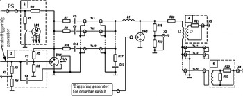
Fig. 7. Electrical scheme of the test bed for tests of the 250/1000 µH coils. PS = HV power supply; 2 = Dump; 3 = HV distributive block; 4 = inductive probe di/dt; 5 = current transformer PEARSON 1423; R7-R16 = protective resistors; С5-С16 = capacitors of the main bank; TL1-TL10 = transmission lines (cable KPV-1/50); L1 = additional inductance; SW1 = main switch; SW2 = crowbar switch, R18-R19 = voltage divider; R20 = additional resistor; L2 = tested 250/1000 µH coil; TL11-TL20 = current divider (cable KPV-1/50).

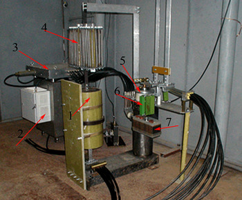
Fig. 8. (Color online) General view of the capacitor bank: 1= capacitors, 2= main switch, 3 = protective resistors.

Fig. 9. Equivalent electrical scheme of discharge circuit of the 250/1000 µH inductor test bed. Li and Ri stand for the inductance and resistance of the 250/1000 µH inductor, C1 = capacitor bank 3100 µF.
Test procedure: For each coil 10 shots were made at 18 kV, 10 shots at 20 kV, and 5 shots at 23 kV with 30 minutes between shots.
Figure 11 shows calculated and experimental traces of the IL4 current and action integral S(I2L4) for charging voltage 23 kV. At 23 kV experimental current and action integral amplitudes are about 70 kA and 32 × 106 A2s, calculated corresponding values are about 67 kA and 30 × 106 A2s.

Fig. 11. (Color online) Experimental (solid blue) and simulation (dashed red) traces of load current Ii and action integral S( $\int\limits_0^t {I_i^2 dt}$) at charging voltage of 23 kV in tests of the 250 µH coils.
Tests of the 1000 µH Inductor
The test bed used was almost the same as in Figure 7. Two identical assemblies (each from four coils) have been made and tested. The first assembly inductance and resistance were 977 µH (measured at 100 Hz) and 20.4 mΩ, for the second one there were 1015 µH and 20.6 mΩ. All parameters are well within 5% required tolerance. Test procedure: Tests were done at charging voltage 18 kV. On the first assembly, 25 shots were made at 28 kA with 10 minutes between shots. It corresponds approximately to case 1 of nominal regime (current is a bit higher here). All waveforms were good and magnetic field measurements were made also during these shots. But during these shots we observed some attractive motion between opposite coils. The assembly was reinforced by inserting square textolite plate inside of the assembly. Twenty-five more shots were made and a new assembly holds on well. On the second inductor, 25 shots also have been done at 28 kA with 10 minutes between shots.
Figure 12 shows calculated and experimental traces of the IL4 current and action integral S(I2L4) for charging voltage 18 kV. At 18 kV, experimental current and action integral amplitudes are about 28 kA and 10 × 106 A2s, calculated corresponding values are about 28 kA and 11 × 106 A2s. About 10 degrees heating was measured on the coils wall after 15 shots at 10 minutes between shots. Calculated inductance here is about 980 µH, it corresponds to measured value. Resistance of the inductors is about 21 mΩ.

Fig. 12. (Color online) Experimental (solid blue) and simulation (dashed red) traces of current (red IL4 and action integral S(I2L4) at charging voltage of 18 kV in tests of the 1000 µH inductors.
Stray Magnetic Field Measurements around the 1000 µH Inductor
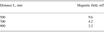
Tests were done at 18 kV charging voltage (current amplitude about 28 kA), three shots at each distance are shown in Tables 3 and 4. Resolution is limited by noise at the 0.1 mT level. Tables 3 and 4 show magnetic field values across and along assembly axis along with calculated values. Notice that measured values are lower than the calculated ones due to many natural metal shields in the experimental room (capacitor bank itself and so on). It may be seen that magnetic field drops very quickly with distance and measured values are about two times lower than the calculated ones, due to cross-interference.
Table 3. Magnetic field across the assembly axis L = 0 – center, L= 530 – coil outer surface
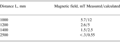
Table 4. Magnetic field along the assembly axis (L = 0 = center)

CONCLUSION
Careful design and a finite element analysis with the ELCUT software was used to build a compact, simple, robust and reliable inductor at 1 mH, which can serve a whole life without n maintenance and satisfy well the requirements for the power conditioning systems. Obtained results on magnetic field and stresses, which the inductor can withstand, are on the edge of nowadays technology. Simulations results agree well with the experimental ones.