


I. INTRODUCTION
First automotive radar sensors in the 76–81 GHz band have been commercially available in the late 1990s. The radio frequency (RF) parts of these sensors typically have been realized using discrete semiconductor devices like GaAs Gunn diodes or Schottky diodes leading to relatively high costs for the sensor system. A step toward higher integration and reduced system costs was the realization of 77 GHz radar components in silicon-based technologies. First radar sensors using a 77 GHz transceiver realized in SiGe bipolar technology [Reference Böck1] are on the market since 2009 [Reference Freundt and Lucas2]. Currently, the 76–81 GHz automotive radar market is relatively small but rapidly growing. The application of actual radar sensors is mainly limited to the premium car segment, because the system costs are still too high for todays low-end cars. One reason for this is the fact that up to now there is no low-cost packaging technology available in the 76–81 GHz band, which can fulfill the requirements of sufficient RF performance at these high frequencies, low-thermal resistance, high reliability for automotive applications, and compatibility with standard automotive board design rules. Therefore, current radar chips have to be applied on the RF sensor frontends using wire-bonding or flip-chip. These techniques are expensive and not compatible with standard mounting of other components on the printed circuit board (PCB) using solder reflow.
In recent years, embedded wafer-level ball grid array (eWLB) technology [Reference Brunnbauer, Fürgut, Beer and Meyer3] has proven to be a low-cost packaging solution with attractive RF performance (e.g. [Reference Wojnowski4]). In this paper, we describe how the eWLB technology can be adapted to fulfill the demanding performance and reliability requirements of automotive radar sensors. In Section II, the most important features of an eWLB package and the process flow for the package fabrication are described. Section III shows the electrical characteristics of transmission lines which can be realized in eWLB technology. Using electromagnetic simulations the transition of the radar chip to the eWLB package and from the package to the PCB is optimized toward minimized losses at 77 GHz. Measures to improve the heat dissipation from the package to the board are described and the reliability of eWLB radar MMICs during temperature cycling on board (TCoB) is investigated. In Section IV, a 77 GHz radar transmitter and a receiver in eWLB package are presented, which are targeting to support next generation low-cost radar sensors for mid-range applications. Finally, a 77 GHz 4-channel radar transceiver with antennas integrated in the eWLB package demonstrates the potential of this technology for future single-chip radar sensors on low-cost standard board materials.
II. eWLB GRID ARRAY PACKAGING PROCESS
Typical dimensions of chip pads with diameters in the range of some 10–100 µm are not compatible with board pitches for automotive applications in the range of 500 µm to 1 mm. To overcome this so-called “interconnection gap” in the eWLB technology the fan-in area of the silicon chip is surrounded by a mold compound which increases the area of the device. This additional fan-out area enables the placement of solder balls on the package in an arrangement which is compatible to standard PCB design rules. The connection of the balls to the chip pads is done by a redistribution layer (RDL) of copper which is embedded in an organic dielectric material. Figure 1 shows a schematic cross-section of an eWLB package. The package thickness is 450 µm. The solder balls consisting of Sn, Ag, and Cu (SAC305) have diameters of 300 µm and pitches of 500 µm. The thicknesses of the dielectric layers and the Cu RDL are in the range of 5–10 µm. Figure 2 shows an eWLB MMIC soldered on a PCB. This illustrates how the fan-out area is used to create connections from chip pads to the board using the RDL and solder balls in the mold area.

Fig. 1. Schematic cross-section of an eWLB package.

Fig. 2. Cross-section of a fabricated eWLB package soldered on a PCB.
The key process of the eWLB technology is the fabrication of a mold wafer with embedded Si chips (Fig. 3). The fabrication starts with a metal carrier which is covered by an adhesive tape. In a next step the diced silicon chips are placed onto the carrier by a pick and place tool with the pad side toward the carrier. Then a liquid mold compound is suspended on the carrier and the mold compound is pressed and cured. After the release of the metal carrier and the laminated tape this results in a wafer consisting of mold compound with the Si chips embedded. These mold wafers are now handled like silicon wafers on typical tools known from standard front-end processing. Photosensitive organic dielectric material is coated and structured by lithography for isolation purposes. A RDL is formed by a galvanic Cu deposition process. An under bump metallization is used to increase the copper thickness underneath the solder balls to improve second-level reliability. After the reflow of the solder balls the mold wafer is separated using conventional blade dicing.

Fig. 3. Process flow for the fabrication of a mold wafer with embedded Si chips.
The most critical process steps for the eWLB technology are the accurate placement of the Si chips on the carrier and the control of the chip position on the mold wafer. To compensate for the shrink of the mold compound during curing an offset correction is done during chip placement. Another important issue can be excess warpage of the mold wafer. This can be critical due to the relatively high flexibility of a mold wafer compared with a silicon substrate. Wafer warpage has to be adjusted by adequate thermal treatment during the different process steps (e.g. curing of the dielectrics on the mold wafer) to ensure correct wafer handling during the complete fabrication sequence.
Since hundreds of packages can be fabricated in parallel on one mold wafer and standard tools known from silicon wafer mass production can be used the eWLB fan-out technology does not only enable new routing concepts but is also cost effective. Typical design rules are 20 µm for minimum Cu RDL width and spacing with tolerances of a few µm. This is small compared with other assembly techniques, e.g., wire bonding with minimum bond length of several 100 µm and tolerances of ±20% in production. Owing to the tight design rules and small tolerances the eWLB package technology is attractive for high-frequency applications like automotive radar. Using eWLB the dimensions of the RDL and its variations can be kept small compared with the wavelength of the electrical signal which is in the mm-range at 77 GHz.
III. PACKAGE CHARACTERISTICS AND OPTIMIZATION
A) Transmission lines in eWLB package
Transmission lines are important building blocks in high-frequency designs. They are used for the signal distribution e.g. from chip to board or for impedance matching. Important design targets are a small form factor, limited attenuation losses, and a wide range of characteristic impedances. Using the RDL of the eWLB package coplanar waveguides (CPW) for single-ended signals can be realized or coplanar strips (CPS) for differential interconnections. A variety of transmission lines have been simulated and fabricated. Figure 4 shows measurements and simulations of the line attenuation and the relative effective permittivity of a 50 Ω CPW. The line attenuation is in the range of 0.3 dB/mm at 80 GHz. This is significantly smaller than the attenuation of transmission lines available on chip which have typically attenuations in the range of 1 dB/mm. The relative effective permittivity is about 2.6 at 80 GHz. With typical line width and spacing in the range of 15–100 µm impedances from about 40 to 140 Ω can be realized. This covers the impedance range usually needed in RF designs. The good line characteristics are due to the low losses of the mold compound and package dielectric and the high Cu thickness of several μm combined with tight design rules. Simulations show that at low frequencies the losses are dominated by losses in the conductor (e.g. 90% at 1 GHz). For higher frequencies the dielectric losses become more and more important. Their contribution to the total losses is in the range of 30–40% at automotive radar frequencies from 76 to 81 GHz. A more detailed characterization of the line characteristics can be found in [Reference Wojnowski5].

Fig. 4. Measured and simulated line attenuation and relative effective permittivity of a 50 Ω CPW realized in eWLB.
B) Optimization of the chip to package to board transition
Critical aspects in mm-wave systems are signal reflections and losses at the interfaces from the semiconductor chip to the package and from the package to the board. The mismatches and the associated losses at these interfaces deteriorate the overall system performance and become more and more dominant with increasing frequency. This is one of the reasons why there is no standard packaging technology with sufficient RF performance available for automotive radar at 76–81 GHz up to now. Best results are still achieved for bare-die wire-bonded chip to board transitions or for flip-chip mounted devices. Typical transmission losses of these techniques are in the range of −2 dB.
eWLB has the potential for good RF performance due to its relatively small design rules compared with standard packaging technologies which enable the realization of short low-loss transitions with high accuracy. However, as the wavelength of only a few mm at 77 GHz is in the same range as the typical dimensions of the package components (package size 6 × 6 mm2, chip size 3 × 3 mm2, ball pitch 0.5 mm, …), a lot of parasitic effects such as cross-talk, reflections, or radiation have to be taken into account. To analyze these effects and to optimize the transitions toward low transmission losses and reflections electromagnetic simulations using the software tools Microwave Studio of CST and HFSS of Ansys have been done.
To study global effects like cross talk between different channels or unwanted radiation of the whole radar system a simulation setup has been created containing the SiGe chip, the most important package components (RDL, dielectrics, mold, and solder balls) and the routing on the PCB. Figure 5 shows the setup for a radar receiver with four single-ended receive channels and a differential LO feed. At the receive channel marked by the red circle a radar signal is applied simulating an incoming signal detected by the antenna. The signal propagation in the whole radar MMIC can now be analyzed. In Fig. 6, the amplitude of the radar signal is indicated by colors ranging from blue for small signals to red for high-signal levels. On the left-hand side a non-optimized board to chip transition is shown. In this case, three vias in the PCB are used to make a ground terminal connection from the PCB via solder balls to the chip. It can be seen that the radar signal is deteriorated by reflections and cross-talk leading to unwanted signals, e.g., at the silicon chip edge or to transmission to a second receiver channel. The total transmission loss is −3 dB in this example which means that half of the incoming radar signal is lost. On the right-hand side an optimized transition is shown with significantly reduced reflections and nearly no cross-talk to the other receiver channels. This is achieved by a simple modification of the ground routing by placement of additional vias on the PCB. The transmission loss is reduced to −1 dB by this measure.

Fig. 5. Simulation setup for a radar receiver with differential LO input and four-single-ended receiver channels (mold compound and dielectric films are not shown, SiGe chip in parts).

Fig. 6. Optimization of a single-ended board to chip transition by positioning of vias on the PCB.
Global simulations have also been used to investigate the signal propagation between different components on the PCB, e.g. between transmitter, receivers, and antennas. It could be shown that a channel isolation higher than 40 dB can be achieved in a realistic radar setup using appropriate chip, package, and board design. Electromagnetic simulations have also been used to investigate the influence of typical fabrication tolerances on system performance. Such parameters are for example variations in the chip or package dimensions, the RDL thickness, deformation of the solder balls during reflow, misplacement of the package on the PCB, or variations in the RDL shielding metallization. It has been found that the eWLB unit on the PCB is not very sensitive on typical process variations resulting in a maximum degradation of the transition loss in the range of 0.5 dB.
After the optimization of the global board, package, and chip design the transition from board to chip has been optimized in detail using a simulation setup with a finer grid for the local transition at the expense of not being able to simulate the whole radar system due to limited computational power. Two cases have been studied: a single-ended ground-signal-ground (GSG) port and a differential transition with a ground-signal-ground--signal-ground (GSGSG) pad configuration on chip. It has been found that the design of the RDL and board lines for both the signals and for the ground planes have major influence on RF performance. By careful design optimization transmission losses of less than 1 dB can be achieved. Figure 7 shows the simulated return and insertion loss for a differential transition as a function of frequency. At 77 GHz a transmission loss of −0.65 dB is achieved with an S11 of approximately −15 dB. Similar results have been obtained for single-ended transitions. These results demonstrate that eWLB technology has very attractive RF performance compared with any other standard packaging technology and enables the use of packaged components at 76–81 GHz with comparable or lower losses than those introduced by other mounting techniques used today in this frequency range like wire-bonding or flip-chip.

Fig. 7. Simulated return and insertion loss of an optimized differential chip to package to board transition (S 21=− 0.65 dB at 77 GHz).
C) Thermal management
The power-added efficiency of radar MMICs at 76–81 GHz is relatively poor, because the cut-off frequencies of the semiconductor devices are not much higher than the system operation frequency and MMICs must be designed near the limit of the given technology. This results in small margin for low-power design. Therefore, a lot of power must be spent to generate the necessary transmit signal in the voltage controlled oscillator (VCO) or to achieve sufficient conversion gain in the receiver part. Typical power consumptions are in the range of 1–2 W for a transmitter or receiver, respectively. To remove the heat associated with this power consumption the thermal resistance of the MMICs must be sufficiently low in order not to exceed typical thermal boundary conditions (e.g. 85°C for the sensor ambient temperature and 125°C for the Si chip bulk temperature). For bare-die chips this can be easily done, because the chips can be glued directly on a thick Cu layer on the PCB. However, for a packaged device the situation is worse, because the heat transfer for a mounted device via the chip backside and radiation to air is rather small. As dielectrics and mold have a high thermal resistance compared with metal or silicon, heat flow occurs mainly via the metal layers and solder material in a mounted device. Therefore, the heat must be conducted via the solder balls to the metal layers on the PCB which are connected thermally to the sensor housing.
In order to investigate and optimize the thermal resistance of radar MMICs in eWLB package finite element simulations using the software tool Ansys have been done. It turned out that balls located on the fan-out area of the package are not very effective in heat transfer due to the long distance from the silicon chip to the solder balls and the limited thickness of the Cu RDL. Solder balls located directly above the silicon chip are much better suited for heat removal. However, as these balls can influence the electromagnetic field in the radar MMIC and deteriorate the chip performance it is often not possible to place solder balls in regions which are important for the RF functionality of the device (e.g. at the VCO core or the power amplifiers at the transmitter outputs or at the mixer cells of the receiver inputs). On the other hand, additional balls with ground termination can support the suppression of parasitic electromagnetic coupling. According to simulation a thermal resistance from the silicon junctions to the solder balls on the PCB of more than 20 K/W for a typical radar MMIC has to be expected without special measures for heat removal. To improve the situation so-called thermal balls have been implemented in the MMIC design. These balls are located in areas of the Si chip which are not critical for the RF functionality (e.g. in the chip corners far away from the RF outputs located in the center of the chip outline). To create the area needed for the ball placement the chip size of the final designs is bigger than needed for the pure electrical functionality. To achieve a low thermal resistance from the balls to the Si chip as much as possible, metal is used underneath the thermal balls in the semiconductor back end of line (BEOL) stack.
In Fig. 8, a simulation example for a transmitter with three channels is shown. Four times four thermal balls are located in the corners of the 3 × 3 mm2 silicon chip. The package dimension is 6 × 6 mm2. It can be seen that the heat is homogenously distributed within the silicon chip despite the fact that the heat is generated locally in hot spots (e.g. in the VCO core). This is due to the high thermal conductivity of silicon. The thermal balls in the chip corners remove the heat from the silicon bulk to the PCB. After layout optimization a thermal resistance of 7.1 K/W for a 77 GHz transmitter and 10.8 K/W for a receiver could be achieved, respectively. This is roughly a factor of 2 smaller than for packaged MMICs without special design measures for heat management.

Fig. 8. Simulated temperature distribution of a three-channel radar transmitter in an eWLB package.
D) Reliability
For safety applications like automotive radar the reliability of the sensor components is of major importance. As the eWLB package technology has initially been developed for consumer applications such as mobile communications with less stringent quality targets, it has been investigated if the eWLB technology can fulfill automotive quality requirements according to AEC-Q-100 standard. In a pre-qualification study, the following stress tests have been performed: pre-conditioning for moisture sensitivity level MSL1, high-temperature storage at 150°C for 1000 h, unbiased humidity accelerated stress test for 96 h, 1000 temperature cycles from −50 to 150°C, 1500 h high-temperature operating life, 1000 cycles power cycling from −40 to 125°C, 1000 h temperature humidity bias at 85°C, 85% r.h. All these tests showed no issues in the electrical performance of the devices after stress. Besides these first-level reliability tests the behavior of devices soldered on the PCB during temperature cycling is important in the sensor application. To investigate this second-level reliability a variety of TCoB stress tests have been performed. To support the development thermo-mechanical simulations have also been done. Usually the thermal expansion of the PCB is higher than the expansion of the packaged device including the silicon chip. This leads to stress in the solder balls during temperature cycling. Finally, the balls can break resulting in a failed electrical connection. This is schematically illustrated in Fig. 9. Not only the package properties are important for TCoB performance, but also the board parameters like board thickness, number of Cu layers, Cu thickness, material for the RF top surface layer on the PCB, etc. After investigation of the most important board parameters by simulation a board stack has been defined which is usable in a real radar sensor and which was used as a reference board for the subsequent optimization of the chip and package design toward improved TCoB reliability. The PCB has a total thickness of 1.0 mm, eight Cu layers, non-solder-mask-defined landing pads, and a 127-μm-thick high-frequency compatible laminate top layer.

Fig. 9. Mechanical stress in solder balls during TCoB.
Important measures in the package design to improve TCoB performance are the use of balls in the package corners without electrical function, because these balls are exposed to the highest mechanical stress during temperature cycling. In addition, as much balls as possible are designed in a redundant manner. This means that the breakage of a ball does not necessarily lead to an electrical fail, because another ball with the same electrical connection is still functional. Only balls in the middle of the package edges with the smallest mechanical stress are designed as non-redundant connections.
From the package technology point of view it turned out that the use of an under bump metallization at the positions of the solder balls is beneficial for the improvement of TCoB reliability. Figure 10 shows failure distributions after TCoB from −40 to 125°C for 1 cycle per hour. It can be seen that with on optimized package design typically 2500–3500 cycles before failure can be achieved without under bump metallization (UBM). Using UBM improves TCoB reliability significantly. The first electrical fail occurs later than 5000 cycles.

Fig. 10. Weibull distribution of electrical failures (in %) after TCoB from −40 to 125°C for radar MMICs in eWLB package with and without UBM.
In the meantime all qualification tests according to automotive quality standard AEC-Q-100 for a transmitter and receiver MMIC have been performed. These results demonstrate that eWLB package technology can fulfill the demanding reliability requirements for automotive radar applications at 76–81 GHz.
IV 77 GHz AUTOMOTIVE RADAR MMICs
A) Transmitter
In this section, a 77 GHz transmitter is described which can support a variety of automotive radar applications. The chip is fabricated in Infineons 0.35 µm SiGe bipolar technology B7HF200 with a maximum oscillation frequency of 250 GHz. The SiGe chip with a size of 3 × 3 mm2 is implemented in a 6 × 6 mm2 eWLB package. The chip contains three output channels which can be used to drive transmit antennas or as local oscillator source for receiver chips. The transmitter is based on a push–push oscillator. The differential VCO output at 77 GHz is buffered and split by two 1:3 power dividers. The block diagram of the transmitter is shown in Fig. 11. The output power can be set individually for each channel using a digital interface. Frequency dividers provide a large range of different divide ratios which can be used for frequency control by a phase-locked-loop (PLL). For the realization of offset PLLs a separate 18 GHz oscillator with low-phase noise and a mixer are implemented, which can be used to downconvert the 19.25 GHz output of the first divider stage of the 77 GHz signal.

Fig. 11. Block diagram of the radar transmitter.
The design goals for the 77 GHz VCO are low-phase noise, linear tuning characteristics with low-tuning sensitivity, and low-frequency pushing. Junction varactors are used for frequency tuning at two inputs (coarse and fine tuning). A total tuning range of more than 7 GHz is achieved with a fine tuning range of more than 3 GHz. An excellent phase noise at 77 GHz is measured with a 1/f corner frequency below 100 kHz. At 100 kHz offset frequency the phase noise is −76 dBc/Hz and varies less than ±1.5 dB over the temperature range of −40 to 125°C. The phase noise of the 18 GHz VCO is −93 dBc/Hz at 100 kHz offset. The output power of each of the 77 GHz channels can be set with 6-bit resolution. A power variation of more than 20 dB is possible with a maximum output power of 11.7 and 9.6 dBm at 25 and 125°C, respectively. Depending on the power setting, the total current of the MMIC is 205 to 710 mA at a supply voltage of 3.3 V.
In Fig. 12, a photograph of the transmitter in eWLB package can be seen. It shows three differential outputs located as close as possible to the SiGe chip to minimize the transition length to the board. Ground guards are shielding the RF ports. Sixteen thermal balls are located on the corners of the SiGe chip for heat removal. All electrical connections are done redundantly using at least two solder balls for the same electrical functionality to improve second-level reliability. Corner balls of the package are without electrical function and improve the mechanical stability of the soldered device. A detailed description of the transmitter is given in [Reference Knapp6].

Fig. 12. Photograph of the three-channel 77 GHz transmitter in eWLB package.
B) Receiver
A 77 GHz four-channel radar receiver has been developed as a counterpart to the transmitter for a complete radar system [Reference Wagner7]. This chip is also fabricated in the B7HF200 SiGe bipolar technology. The chip and package size are the same as for the transmitter, but the ball population is changed to enable the necessary I/O configuration. The four receive channels have single-ended inputs. A differential LO input can be driven by one of the transmitter outputs. Again the RF critical transitions are positioned as close as possible to the SiGe chip to minimize transition losses. As in the transmitter design 16 thermal balls are used for heat removal; however, their placement is different due to the different location of RF critical parts in the two MMICs (Fig. 13).

Fig. 13. Photograph of the four-channel 77 GHz radar receiver in eWLB package.
The chip operates with a supply voltage of 3.3 V. Besides typical receiver RF design targets like high conversion gain, low noise, and minimized power consumption, special care has been taken to implement self-test features in the MMIC. The control of the correct functionality of the radar components in the system is an important step toward radar safety applications. To address this issue the receiver contains a test signal generator which allows e.g. to measure the amplitude and phase relationships between all four receive channels. As in the transmitter an on-chip temperature sensor is implemented to enable the temperature monitoring of the MMIC in the application. This can prevent reliability issues, because the operation of the chip out of the specified temperature range can be avoided.
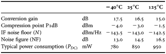
The key parameters of the receiver are given in Table 1 for a temperature range of −40 to 125°C. As a figure-of-merit (FOM) for radar systems, FOM = G C – N + P TX can be defined where G C and N are the receiver conversion gain and IF noise floor, respectively, and P TX is the output power of the transmitter. A FOM of 171.2 dB is achieved for the two presented MMICs. This demonstrates that these packaged devices offer attractive device performance and will enable the first automotive radar systems using silicon-based packaged devices in the frequency range from 76 to 81 GHz, which can be mounted on the system PCB using standard solder reflow [Reference Knapp6–Reference Trotta8]. This is an important step for further cost reduction in automotive radar systems in this frequency range and will enable low-cost radar sensors even for the low-end car segment in the near future.
Table 1. Typical characterization results of the four-channel receiver in eWLB package.
C) Radar MMICs with antennas in package
Owing to the high losses of standard PCB materials (e.g. FR4) for radar signals in the frequency range from 76 to 81 GHz low-loss RF compatible substrate top-layers are used in actual radar boards in order to minimize transmission losses of the signals on their way from the transmitter to the antennas or from the antennas to the receiver. RF substrates are expensive and the manufacturability of those materials is difficult and often not compatible to standard laminate processes. Therefore, it would be of great interest to integrate the antennas of a radar system into the package of the MMICs. This would eliminate the need for a high-frequency transition from the package to the PCB, because the radar signal could be directly radiated from the device. In this case, low-cost standard boards could be used, because only DC or low-frequency connections between PCB and MMIC would be necessary. There have been attempts to integrate antennas directly on the silicon radar chip. However, this approach leads to high chip costs, because the area of the antennas is in the range of several mm2 and the efficiency is not very high due to the high RF losses of silicon substrates. eWLB technology can enable a potential low-cost integration of antennas into the package, because the antennas can be placed on the fan-out area consisting of inexpensive mold compound (Fig. 14). The antennas are realized using the Cu RDL of the package process. Owing to the decoupling of the antenna position from the Si chip losses in the silicon substrate can be kept low. A reflector in the top metal layer of the PCB can be implemented to improve the radiation toward the intended direction of the radar signal. In addition, this makes the performance of the radar system independent from the properties of the PCB material.

Fig. 14. Radar MMIC with antennas integrated in the eWLB package.
A variety of antenna types have been simulated and tested in eWLB package runs. Figure 15 shows some examples like dipole antennas, arrays of dipoles with additional reflectors realized in the RDL, or CPW patches. Reasonable agreement between simulation and measurements was found. Typical antenna gains are in the range of 5–10 dBi. Finally, the feasibility of a complete four-channel radar transceiver with antennas in package has been investigated. Four dipole antennas have been integrated on the mold compound of a eWLB package together with a 77 GHz radar transceiver chip realized in SiGe bipolar technology (Fig. 16). The package dimension is 8 × 8 mm2. The functionality of the radar system with antennas integrated in package has been tested and characterized in a laboratory environment. Details on the system design and measurement results can be found in [Reference Wojnowski, Wagner, Lachner, Böck, Sommer and Pressel9]. The measured and simulated radiation patterns of the radar system show reasonable agreement. The demonstrated radar functionality with integrated antennas could be attractive for future low-cost sensors like short range automotive radar but also for industrial applications.

Fig. 15. Photographs of different antennas realized in the RDL of the eWLB package: dipole (left), array of two dipoles with reflectors (center), and CPW patch (right).

Fig. 16. Photograph of the four-channel 77 GHz radar transceiver with antennas integrated in package (8 × 8 mm2).
V CONCLUSION
Embedded wafer-level ball grid array (eWLB) has been investigated as a potential low-cost packaging technology for 76–81 GHz automotive radar applications. By carefully optimizing the chip and package design and the package to board transition low transmission losses of less than 1 dB have been achieved. The MMIC design has been optimized for effective heat removal from the packaged devices. The package process and the design have been improved to achieve automotive quality requirements according to AEC-Q-100 standards and to optimize the reliability during TCoB. 77 GHz transmitter and receiver components in eWLB package have been developed. These devices show excellent RF performance and can be applied on a PCB using standard solder reflow assembly techniques. This will enable the first automotive radar sensors in the 76–81 GHz range using low-cost MMICs in plastic package. The potential of eWLB technology for further system cost reduction is demonstrated by a four-channel radar transceiver with antennas integrated in package. Therefore, eWLB package technology is very attractive for future automotive radar systems to be used even in the low-price car segment. It will enable radar safety functions which are affordable for everyone.
Acknowledgement
Parts of this work have been funded by the German “Bundesministerium für Bildung und Forschung” (BMBF) under contract 13N9822 “Radar on Chips for Cars” (RoCC).
 Josef Böck received a diploma degree in physics and his Ph.D. from the University of Regensburg, Germany in 1994 and 1997, respectively. In 1993, he joined the Corporate Research of Siemens AG in Munich, Germany. He was working on characterization and technology development of Si and SiGe bipolar devices for mobile communications and high-speed datalinks. Since 1999, he is with Infineon Technologies. Currently, he is engaged in process integration for SiGe BiCMOS technology and packaging techniques for automotive radar applications.
 Maciej Wojnowski received the M.Sc. degree in microwave engineering from the Technical University of Gdansk, Gdansk, Poland, and the Ph.D. degree from the University of Erlangen-Nuremberg, Erlangen, Germany, in 2004 and 2011, respectively. He has been with Infineon Technologies AG, Munich, Germany, since 2005. He was responsible for electrical characterization and modeling of the eWLB technology for system-in-package applications. He is the author or co-author of more than 30 papers in the areas of high-frequency packaging and measurement techniques. His current research interests include high-frequency package characterization and modeling, signal integrity, calibration and de-embedding techniques for interconnect and passive device characterization, and computational electromagnetics.
 Christoph Wagner received the M.Sc. degree in mechatronics from the Johannes Kepler University, Linz, Austria in 2006, and is currently working toward the Ph.D. degree at the Johannes Kepler University. In 2006, he joined Danube Integrated Circuit Engineering (DICE) in Linz, Austria. In 2007, he became a member of the Christian Doppler Laboratory for Integrated Radar Sensors, Johannes Kepler University. Since 2010, he is with DICE, Linz, Austria, where he is responsible for radar MMIC development in the microwave and millimeter wave frequency range.
 Herbert Knapp received the Diploma and Ph.D. degrees in Electrical Engineering from the Technical University Vienna, Austria, in 1997 and 2000, respectively. In 1993, he joined Siemens, Corporate Technology in Munich, Germany, where he worked on circuits for wireless communications and high-speed data transmission. He is now with Infineon Technologies, Munich, Germany, and is engaged in the design of circuits for automotive radar applications.
 Walter Hartner received his Diploma in Physics from the Friedrich-Alexander University of Erlangen in 1995 and his Ph.D. in Electrical Engineering from the Technical University of Aachen in 2003. He has authored and co-authored more than 25 articles and he holds more than 40 patents. His current development interests are in wafer-level package technologies.
 Markus Treml received his diploma in 2005 from the Technical University of Graz and received his Ph.D. at the Johannes Kepler University Linz in 2010. He is currently a development engineer with Danube Integrated Circuit Engineering GmbH & Co KG, Linz, Austria. His main research interests are automotive radar systems and mm-wave packages.
 F. J. Schmückle received the Dipl.-Ing. (FH), Dipl.-Ing. (TH) and Dr.-Ing. (Ph.D.) degrees in 1980, 1985, and 1991, respectively, from the FH Wiesbaden, the Technical University of Darmstadt, and the FernUniversität Hagen, Germany. Since 1994, he is with the Ferdinand-Braun-Institut at Berlin, Germany, as a research engineer in the microwave department. His present research activities focus on electromagnetic simulations, mainly in the field of microwave packaging emphasizing on transitions as e.g. flip-chip technologies, Ball Grid Array (BGA) submounts, transitions from hollow waveguides to MS, measurement probes, and calibration sets.
 Siddhartha Sinha received his Bachelor Degree in Electronics and Communication Engineering from PESIT Bangalore, India. He then worked for 2.5 years as a Scientist-B in Microwave Tube R&D Centre, a constituent laboratory of the Defense R&D Organization of India. Thereafter he received his Master Degree in Microwave Engineering from the Technical University Munich, Germany. Presently, he is pursuing his doctoral degree from the Ferdinand-Braun-Institute for High Frequency Technology in Berlin, Germany. His interests are microwave and mm-wave interconnects, mm-wave packaging and optimization, equivalent circuit description of microwave transitions, and computational electromagnetics.
 Rudolf Lachner received the diploma and Ph.D. degrees in Physics from Technical University Munich, Germany, in 1978 and 1984, respectively. He joined Infineon Technologies in 1984 where he first was engaged in process development and integration of high-speed bipolar processes. Later on he took over the responsibility for the development of Infineons leading edge Silicon and Silicon-Germanium bipolar and BiCMOS processes. As a Senior Principal in the field of RF technologies his main interests are currently in pushing the limits of SiGe technology into the Terahertz region and paving the way to broad usage of Si based mm-wave technology in new safety and communication applications. He has filed several patents and authored or co-authored many publications in this field.


