I. INTRODUCTION
Filter devices for mobile and wireless applications in radiofrequency (RF) require the use of insulating substrates to reduce the electrical losses in the substrate. Thus, the main substrates employed for the passive component integration are glass, sapphire, or high resistivity silicon (HR Si). Nevertheless, a monolithic integration of both the passive and the active devices is impossible on these substrates and silicon is commonly used. However, it is responsible for high substrate losses at high frequency and for the decrease of passive devices performances.
The silicon/porous silicon (PS) hybrid substrate is a serious alternative to silicon for the monolithic integration of RF circuits. PS is known for its insulating properties. Indeed, Balagurov and Timoshenko report mesoporous silicon conductivity σ PS of 10−7 (Ω.cm)−1 in direct current (DC) [Reference Balagurov1, Reference Yu2]. However, σ PS increases with frequency. Ben-Chorin has measured a conductivity modification from 10−8 to 10−5 (Ω.cm)−1 from DC signal to 10 kHz [Reference Ben-Chorin3]. In addition, PS has a porosity-dependant permittivity ε PS ranging between 2 and 11.7. Indeed, experimental values reported in the literature have already confirmed the linear decrease of ε PS with the porosity [Reference Issa4].
PS can be used as a substrate for microelectronic applications. Numerous authors show interest in PS for passive components integration such as inductors [Reference Capelle5], coplanar waveguides (CPWs) [Reference Sarafis6], and filters [Reference Lee7]. In addition, PS can be used to reduce capacitive coupling with the substrate under bump pads [Reference Chong8] or to avoid crosstalks between the components through silicon [Reference Kim9]. If the PS is fabricated locally, it can be employed as a sacrificial layer for the MicroElectroMechanical Systems (MEMS) process [Reference Hedrich10] or active devices can be also integrated on the silicon regions of the hybrid substrate.
In this study, PS areas are fabricated locally on a p+ silicon substrate for the monolithic integration of RF circuits. To quantify the effect of PS on the losses reduction, CPWs have been integrated. The performances of these devices have been extracted from the measured S parameters and compared with bulk substrates such as glass, HR Si, and low resistivity silicon (LR Si). In addition, to evaluate the effect of PS thickness, 20, 50, and 160 µm-depth PS layers have been fabricated on the entire surface of the wafer and have been characterized. These substrates will be called later “full wafer PS”.
This work shows that the insulating PS areas allow improvement of the CPW performances by reducing the substrate losses in comparison with bulk HR Si.
II. DEVICES INTEGRATION
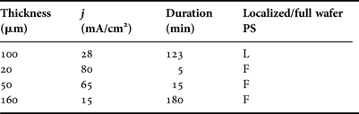
A) PS fabrication
Both localized PS and full wafer PS have been fabricated by the anodization of a p-type silicon wafer (ρ = 20 mΩ.cm) in an electrolyte composed of 30% hydrofluoric acid, acetic acid, and water. PS thicknesses from 20 to 160 µm have been obtained by using the anodization conditions detailed in Table 1. The average porosity measured by gravimetry [Reference Brumhead11] is between 40 and 50% in function of the current density applied. The PS obtained is mesoporous with strongly interconnected pores oriented perpendicularly to the surface (Fig. 1(a)). The pore diameters are from 7 to 10 nm.

Fig. 1. (a) Scanning electron microscope cross section of the mesoporous silicon obtained. Pores are strongly interconnected. (b) Cross section of a localized PS area after the etching of the fluoropolymer mask.
Table 1. Anodization conditions used to fabricate localized and full wafer PS silicon substrates.
PS localization has been performed with an inert fluoropolymer hard mask [Reference Defforge12]. After the anodization, the mask has been etched with an O2 plasma without damaging the PS surface. The PS region obtained has a rounded etching profile (Fig. 1(b)). This shape is a consequence of the anisotropy of PS fabrication [Reference Astrova13]. Then, the substrate has been annealed at 300°C under N2 for 1 h in order to stabilize the structure.
Once PS is fabricated, a 500 nm oxide is deposited on the surface as a cap layer and the component is integrated on the substrate.
B) Devices fabrication
CPWs have been integrated on HR Si (ρ = 3 kΩ.cm), LR Si (ρ = 20 mΩ.cm), glass, and PS substrates (Fig. 2). In the case of the localized PS substrate, both the pads and the lines are integrated on the PS region. The CPWs are made of a 1 µm-thick aluminum layer (ρ = 3.2 × 10⁻⁶ Ω.cm) deposited by physical vapor deposition at 350°C.
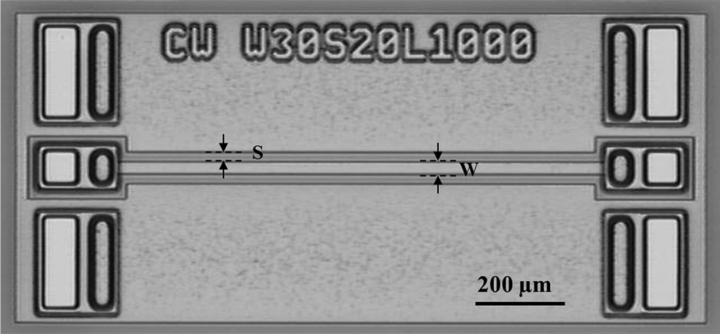
Fig. 2. Typical CPW integrated on PS, glass, and silicon. S and W are respectively the distance line to the ground and the line width.
The distance between the line and the ground plane (S) is 20 µm, the width (W) is equal to 10 or 70 µm and the length (L) is equal to 1000 or 1500 µm. For instance, a 30 µm-wide CPW, with a length and distance to ground respectively equal to 1500 and 20 µm is called W30S20L1500.
III. DEVICES CHARACTERIZATION
The devices have been characterized up to 20 GHz. The measures of the S parameters have been performed on the different substrates (HR Si, LR Si, glass, full wafer PS, and localized PS) with a network analyzer previously calibrated with the Short Open Load Thru (SOLT) method. The PS thicknesses investigated are 20, 50, 100, and 160 µm
To reduce the noises due to the measurement, the two lines extraction method has been used [Reference Mangan14]. The de-embedding is performed thanks to the measurements of two lines of different lengths (1000 and 1500 µm). First, the S parameters are measured and converted to an ABCD chain matrix. They are respectively called C 1 and C 2 for the 1500 µm (l 1) and 1000 µm (l 2) long CPW. C 1 and C 2 can be decomposed into a cascade of three two-port networks consisting of two pads (P 1 and P 2) and the intrinsic device L (1, 2).
 $$C_1=\lsqb P_1\rsqb \lsqb L_1\rsqb \lsqb P_2\rsqb$$
 $$C_2=\lsqb P_1\rsqb \lsqb L_2\rsqb \lsqb P_2\rsqb$$
The multiplication of C 1 by the inverse of C 2 gives (3) where L 1–2 (4) is the matrix corresponding to the ABCD chain of an intrinsic line with a length equal to Δl = l 1 − l 2 [Reference Dworsky15]. Z C is the characteristic impedance and γ is the propagation constant.
 $$\eqalign{\lsqb C_1\rsqb \lsqb C_2\rsqb ^{-1} & =\lsqb P_1\rsqb \lsqb L_1\rsqb \lsqb P_2\rsqb \times \lsqb P_2\rsqb ^{-1}\lsqb L_2\rsqb ^{-1}\lsqb P_1\rsqb ^{-1} \cr & =\lsqb P_1\rsqb \lsqb L_{1-2}\rsqb \lsqb P_1\rsqb ^{-1}}$$
 $$L_{1-2}=\left[\matrix{ cosh\lpar \gamma.\Delta l\rpar & Zc. sinh\lpar \gamma. \Delta l\rpar \hfill \cr {1\over Zc}.sinh\lpar \gamma. \Delta l\rpar & cosh\lpar \gamma.\Delta l\rpar \hfill}\right]$$
As [P 1] and [P 2] are invertible matrices and [L 1–2] a square matrix of the same order, (5) can be deduced. The trace T can be calculated from C 1 and C 2 (deduced from the S parameters measurements). The propagation constant γ of the intrinsic line can be determined (6).
 $$\eqalign{T=Trace\lpar \lsqb C_1\rsqb \lsqb C_2\rsqb ^{-1}\rpar & = Trace\lpar \lsqb L_{1-2}\rsqb \rpar \cr & =2.cosh\lpar \gamma.\Delta l\rpar }$$
 $$\gamma={1 \over \Delta l}.cosh^{-1} \lpar T/2\rpar$$
The real part of γ represents the attenuation constant α which is a function of the radiation losses, losses in the metal line (conductor losses), and in the substrate (dielectric losses). For this study, the radiation losses are neglected. The imaginary part β corresponds to the phase constant.
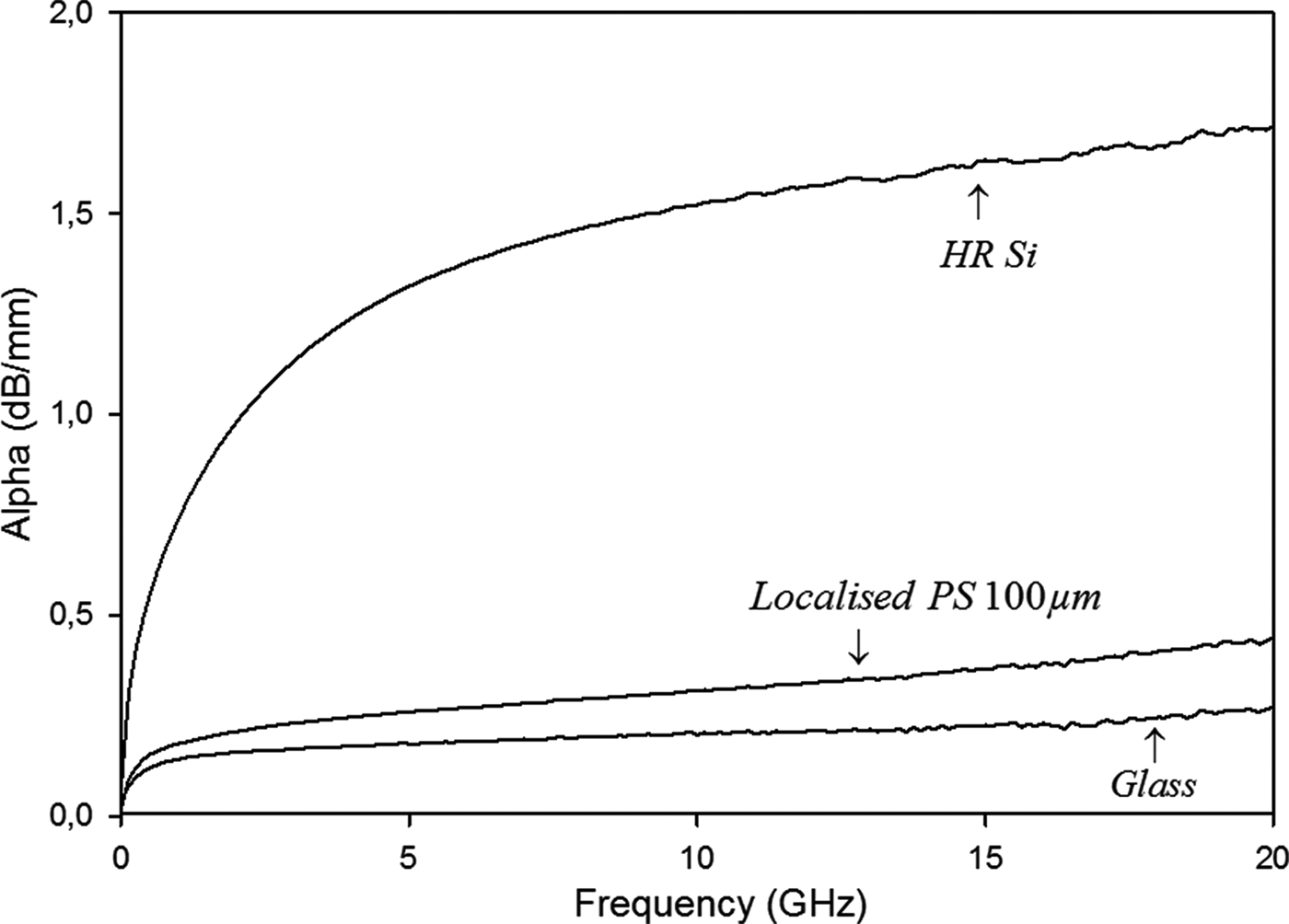
By this method, the effect of the substrate on the attenuation constant is studied by observing the evolution of α with the frequency up to 20 GHz (Fig. 3). It is assumed that the CPW metal losses are similar with all the substrates since the same process has been conducted. The attenuation constants measured at 20 GHz are respectively 1.73, 0.43, and 0.27 dB/mm with HR Si, localized PS, and glass substrates. This result shows that PS reduces losses in the substrate in the RF field regarding silicon.
Fig. 3. Evolution of the attenuation constant α of a W10S20L500 CPW with the frequency. The devices are integrated on glass, HR Si, and localized PS.
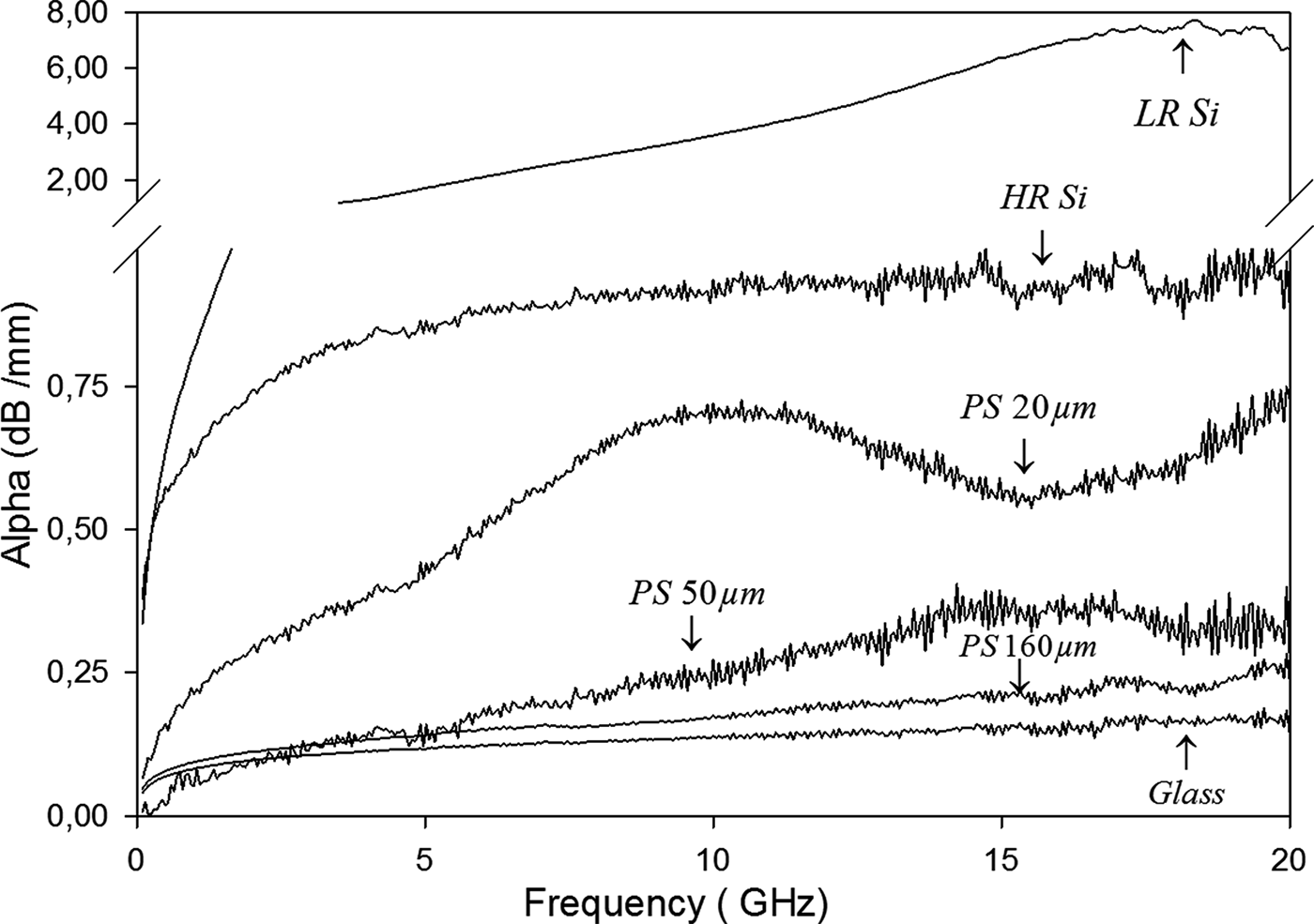
In order to observe the effect of PS thickness on the attenuation constant, a W70S20L500 CPW has been integrated on full wafer PS substrates. The investigated PS thicknesses are 20, 50, and 160 µm. The characterization results have been compared to the one obtained on the reference substrates (Fig. 4).
Fig. 4. Evolution of the attenuation constant α of a W70S20L500 CPW with the frequency. The devices are integrated on glass, HR Si, LR Si and PS substrates (layers thicknesses are 20, 50, and 160 µm).
A high decrease of the substrate losses is obtained with the increase of PS thickness. Thus, attenuation constants of 0.23, 0.34, and 0.7 dB/mm have been measured respectively on 160, 50, and 20 µm-thick PS at 20 GHz. At the same frequency, higher losses have been observed with the bulk silicon substrates since α is equal to 0.9 dB/mm on HR Si and 6 dB/mm on LR Si. The smallest constant attenuation has been obtained with the glass substrate (0.16 dB/mm) because this material possesses a smaller permittivity and higher resistivity than PS.
According to the results obtained on full wafer PS substrates, it can be assumed that the same trend would be obtained with a localized PS substrate. Thus, the CPW losses can be reduced by increasing the depth of the PS regions.
In comparison with silicon, the lowering of the attenuation constant α is linked to the decrease of losses in the PS substrate. This is explained by the insulating properties of the PS used here as a substrate. In fact, the calculated relative permittivity of the PS fabricated is between 6 and 7.5 (respectively for porosities of 50 and 40%). In addition, the resistivity of mesoporous silicon used is close to a few kΩ.cm [Reference Sarafis6]. That is why less electrical or magnetic energy is dissipated in the PS substrate than in silicon and the dielectric attenuation constant is decreased.
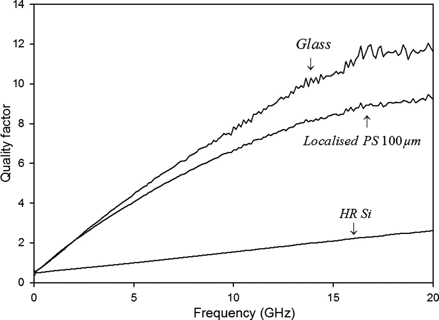
Then, the quality factor Q of the CPW is studied. It corresponds to the ratio of the stored energy to the dissipated power (7) [Reference Bahl16]. The Q factor expresses the energy losses in the component taking into account the phase constant. Higher is the Q factor, better are the CPW performances. Usually, the CPW is used at the frequency where the Q factor is maximum.
 $$Q=\omega{\hbox{Stored energy} \over \hbox{Dissipated power}}$$
For a CPW, the Q factor is calculated from the attenuation constant α and the phase constant β (8).
 $$Q={\beta \over 2 \alpha}$$
The Q factors of the CPW integrated on the localized PS and the reference substrates are shown in Fig. 5. The highest Q factor (12 at 20 GHz) is obtained with the glass substrate. Its value on localized PS is 9.4 whereas it is equal to 2.6 on HR Si at 20 GHz. Thus, with the integration of the line on the localized PS, the Q factor is improved by more than 200% at 20 GHz in comparison with HR Si.
Fig. 5. Evolution of aW10S20L500 CPW Q factor with the frequency. The devices are integrated on glass, HR Si, and localized PS. The Q factor is improved by more than 200% at 20 GHz with PS in comparison with HR Si.
Finally, the losses in the substrate are reduced with PS regarding HR Si. The best performances are obtained with the glass substrate which possesses better insulating properties than PS. However, the active devices cannot be integrated on the glass substrate when compared to the hybrid substrates.
Similar studies have been conducted in the literature but few focus on localized PS and make comparison with HR Si. However, it is shown that the CPW performances on PS can be improved by increasing the porosity, thickness, or by PS oxidation. Thus, Sarafis et al's work on aluminum CPW integrated 150 µm-thick PS with porosities from 70 to 80% [Reference Sarafis6]. They obtained α and Q factor respectively equal to 0.15 dB/mm and 15 at 25 GHz. Then, an α of 1.5 dB/mm has been measured on 20 µm-thick oxidized PS whereas losses on silicon were 13.5 dB/mm at 35 GHz [Reference Welty17].
IV. CONCLUSION
In this work, the interest of the Si/PS hybrid substrate for the monolithic integration of RF circuits has been shown. Insulating PS regions have been fabricated on a p+ silicon substrate through a fluoropolymer mask. CPWs have then been integrated on the PS areas and characterized. The results have been compared to the one obtained on the glass, HR, and LR Si substrates.
The two lines method has been used to reduce the measurement noises and characterize an intrinsic line.
The results obtained have demonstrated that the substrate losses are reduced with PS regarding HR Si. Thus, the Q factor is improved by more than 200% and α is decreased by 1.3 dB/mm at 20 GHz with the localized PS substrate.
The silicon/PS hybrid substrate appears here as an alternative solution to silicon for the monolithic integration of RF systems since it provides a better integration rate, improves passive devices performances, and is compatible with CMOS industrial processes.
 Marie Capelle received the Engineering diploma in physics from the Institut National des Sciences Appliquées, Toulouse, France, in 2010. She is currently working toward the Ph.D. degree with the Laboratoire de Microélectronique de Puissance, Université de Tours and STMicroelectronics Tours, France. Her current research interests include the integration of active and passive devices on hybrid substrates of silicon and porous silicon.
 Jérome Billoué received the M.Sc. degree in telecommunications from the Université de Poitiers, Poitiers, France, in 2004 and the Ph.D. degree in electronic and engineering science from the Université François Rabelais, Tours, France, in 2007. He is currently an Associate Professor with the GREMAN, Université de Tours. His current research interests include radiofrequency passive devices design, modeling, and characterization.
Patrick Poveda was born in 1970. He received the Ph.D. degree in Materials Sciences from the University of Aix-Marseille 2, Marseille, France, in 1997. He worked for several years on RF diodes development and qualification as R&D Device engineer and is the author of several patents on this topics. He is currently R&D Integration Manager with STMicroelectronics, Tours, France. His research interests include the integration of passive and active devices for surge and ESD protection, filtering, decoupling, and RF applications.
 Gael Gautier was born in 1976. He received the Engineering diploma in optoelectronics and the M.Res. degree in fundamental physics from the Institut National des Sciences Appliquées de Rennes, Rennes, France, in 1999 and the Ph.D. degree in microelectronics from the University of Rennes I, Rennes, in 2002. He is the author or coauthor of more than 40 peer-reviewed articles in the field of thin-film transistors and porous silicon. His research interests include the study of the electrochemical synthesis of innovative materials for microelectronic devices, particularly porous silicon.