


I. INTRODUCTION
As the demand for wireless communications continues to grow, the requirement of high-efficiency, high-frequency power amplifiers has never been greater. The operating and deployment costs of wireless base stations and the mobility of user terminals can be significantly optimized by increasing the efficiency of the power amplifiers in the final output stage.
Unfortunately, there is often a trade-off between amplifier efficiency and amplifier linearity. To fulfill the stringent linearity requirements of wireless communication standards while achieving high efficiency, designers propose some advanced transmitter architectures, such as linear amplification using non-linear components (LINC) [Reference Huttunen and Kaunisto1], envelope elimination and restoration [Reference Diet, Berland, Villegas and Baudoin2], and polar amplifiers [Reference Pedro, Garcia and Cabral3]. It is generally believed that switching-mode power amplifiers that can offer unity theoretical efficiency are the most promising solution in these transmitter architectures.
Class E [Reference Sokal and Sokal4–Reference You, He, Tang and Cao6] and class F [Reference Raab7] are two well-known switching-mode power amplifier topologies that have demonstrated high performance at radio and microwave frequencies, whereas there are some limitations when designing them. Class E amplifier's high drain voltage is very dangerous to the transistor's safety, and class F amplifier needs complex tuned circuits to supply open and short circuits to the alternating harmonics. To address these limitations, some new designs that unify class E and class F or class 1/F [Reference Wei8, Reference Inoue9] into a single framework were proposed [Reference Kee, Aoki and Rutledge10–Reference Grebennikov14]. It is a pity that these literatures have not introduced exact design equations or simple design process of the class FE and class E/F power amplifier topologies. In 2005, a new topology for the class E amplifier has been reported by T. Mury. Termed as the inverse class E amplifier it has several advantages over the classical class E configuration [Reference Mury and Fusco15–Reference Mury and Fusco18]. For example, when compared with the classic class E topology the inverse class E amplifier offers (i) lower inductance values, which is more attractive for lumped MMIC implementation, (ii) better harmonic suppression when operated into a distributed load network, and (iii) lower peak switching voltages, which reduces the possibility of the device failure owing to transistor breakdown mechanisms [Reference Mury and Fusco17, Reference Mury and Fusco18]. However, the inverse class E amplifier does not further the power output capability and has higher drain current when compared with the class E mode. A modified class E amplifier with tunable serial–parallel resonator network that replaces the single parallel capacitor of the classic class E mode was proposed in [Reference You, He, Tang and Cao6]. The results have shown that the modified topology is able to improve the power output capability, whereas the proposed circuit also has high drain voltage.
In this paper, we have introduced a tunable parallel resonant tank into the load network of the inverse class E amplifier. The new configuration is similar to a hybrid combining features of inverse class E and class F or class1/F, and demonstrates varying degrees of trade-off between the peak drain voltage and current when the added parallel resonant is tuned to the different frequency. The proposed amplifier not only maintains the zero power loss switching operation, but also brings in some improvements, such as higher output power, power output capability, and further relaxes design requirements. This paper is organized as follows: In Section II, the theoretical analysis and the design equations for the new topology operating under ideal switching conditions are given in detail. Section III will present amplifier's performance supported by numerical results when the added parallel resonant tank tuned to the different frequencies. In Section IV, circuit harmonic balance simulations and experiments are carried out to validate the theories. And Section V presents the conclusion.
II. FUNDAMENTAL THEORY
Figure 1 depicts the circuit schematic diagram of the amplifier proposed in this paper. The transistor operates cyclically as an ideal switch at the fundamental frequency (ω); the load network is similar to the inverse class E amplifier, but it has a more parallel resonant tank C n //L n, the resonance frequency of this parallel resonant circuit is nω, where n is a design parameter and it can be set to any value. When n is an integer, the impedance of the parallel-tuned circuit C n//L n is infinite at the frequency nω and zero otherwise. Especially this new configuration open circuits the second harmonic which is similar to the inverse class F amplifier when n = 2, and open circuits the third harmonic that is similar to the class F amplifier when n = 3. Thus, the modified class E amplifier proposed in this paper exhibits different performance with design parameter n varies.

Fig. 1. The circuit schematic diagram of the proposed inverse class E amplifier with series tunable parallel resonant tank.
The analysis of the circuit is based on the following assumptions that are proposed by the previous literature [Reference Mury and Fusco15]: (i) The transistor is modeled as an ideal switch; the switching action of the transistor is instantaneous and lossless. (ii) The switch duty cycle is 50%. (iii) The RF choke (RFC) has an infinite inductance; The DC block has an infinite capacitance. (iv) The factor Q L of the parallel LC resonator is high enough so that the output voltage is essentially sinusoidal at the carrier frequency.
A) Switch current and voltage steady-state waveforms
According to the assumptions above, the output voltage and the output current are sinusoidal and are defined as
where θ = ωt, ω = 2π f o (f o is the fundamental frequency), the switch is closed when 0 ≤ θ < π ; and the switch is opened when π ≤ θ ≤ 2π. V DC is a DC input voltage, φ is the phase angle of the output signal, and R L is the load resistance. Parameters a and φ are to be determined. From Fig. 1, according to the KVL law v 1(θ) can be expressed as
And then, the steady-state switch current and voltage waveforms can be expressed as
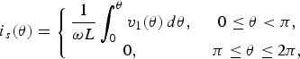
According to the KCL law, the current through switch i s(θ) can be rewritten as
and the current i 2(θ) flowing through the parallel resonant tank C n//L n can be expressed as
Hence, when the switch is ON (0 ≤ θ < π), from (4), (6) and (7), we obtain
Equation (8) can be represented in the form of the second-order differential equation given by
Substituting (3) into (9), results in
the general solution of which can be obtained by

where ![]() , and coefficients A 1, A 2 are yet to be determined.
, and coefficients A 1, A 2 are yet to be determined.
Under the initial condition i s(0) = 0, substituting (11) into (4), the steady-state switch current waveform is then given by
![\eqalign{& i_s \lpar \theta \rpar \cr &=\left\{\matrix{\displaystyle{1 \over \omega L} \left[\matrix{A_1 {\displaystyle{\sin \lpar \beta \theta \rpar \over \beta }} - {\displaystyle {A_2 {\cos \lpar \beta \theta \rpar - 1 \over \beta }}} \cr + {\displaystyle{n^2 V_{DC} \theta \over \beta^2}} \cr + {\displaystyle{{aV_{DC} \lpar \cos \lpar \theta + \varphi\rpar - \cos \varphi \rpar \lpar n^2 - 1\rpar } \over \beta^2 - 1}}} \right]\comma \; &0 \leq \theta\lt \pi\comma \; \cr 0\comma \; &\pi \leq \theta \leq 2\pi.} \right.}](https://static.cambridge.org/binary/version/id/urn:cambridge.org:id:binary:20151022075450975-0612:S1759078711000250_eqn12.gif?pub-status=live)
When the switch is OFF (π ≤ θ ≤ 2π), according to the KCL law i 2(θ) + I DC = 0, we obtain
Equation (13) can be represented in the form of the second-order differential equation given by
Substituting (3) into (14), results in
which general solution can be obtained by
where π ≤ θ ≤ 2π, and coefficients A 1′, A 2′ are yet to be determined. Substituting (16) into (5), the steady-state switch voltage waveform is then given by

In summary, the switch current and voltage steady-state waveforms can be obtained from (12) and (17), respectively. And all the unknown parameters in these expressions will be calculated in the following analysis.
B) ZCS conditions of inverse class E power amplifier
For the lossless operation mode, it is necessary to provide optimum conditions to eliminate power losses of the transistor. The zero-current switching and zero-current slope switching conditions (i s(π) = 0; i s′(π) = 0) should be fulfilled. As a result, we obtain two equations:

Combining (18) and (19), A 1 and A 2 can be expressed as two equations with three unknown parameters (a, β, φ):


C) The continuity of the capacitance voltage and inductance current
The energy stored in capacitance or inductance cannot change instantly, and hence the voltage across the C n or the current through the L n is continuous. According to the continuity of the capacitance voltage and inductance current, we obtain some other boundary conditions besides the ZCS conditions.
Since the voltage v 2(θ) across the C n is continuous, v 1(θ) is also continuous. From zero-current slope switching condition (i s′(π) = 0) and the continuity of v 1(θ), we obtain v 1(π) = 0, then combine it and (16), results in
When θ = π, equation (13) can be written as ωC nv 2′(π) + I DC = 0, then substituting (3) and (17) into it, we obtain
From (22) and (23), A 1′ and A 2′ can be expressed as two equations with three unknown parameters (a, β, φ):
There is another equation v 1(0) = v 1(2π) since the voltage v 2(θ) across the C n is continuous. Combine it and (16), results in

In addition, it is necessary to consider the continuity of current i Ln(θ) through the L n to determine all the unknown parameters. The expression of i Ln(θ) during a whole cycle (0 ≤ θ ≤ 2π) is given by
![\eqalign{& i_{L_n } \lpar \theta \rpar \cr & = \left\{\matrix{\displaystyle{1 \over \omega L_n} \vint_0^{\theta} \left[\matrix{ - A_1 \cos \lpar \beta \theta \rpar - A_2 \sin \lpar \beta \theta \rpar \cr + \displaystyle{\lpar \beta^2 - n^2 \rpar V_{DC} \over \beta^2} \cr + \displaystyle{aV_{dc} \lpar n^2 - \beta^2 \rpar \sin \lpar \theta + \varphi \rpar \over \lpar \beta^2 - 1\rpar }} \right]\, d\theta\comma \; \hfill &0 \leq \theta\lt \pi\comma \; \hfill \cr \displaystyle{1 \over \omega L_n} \vint_\pi^{\theta} \left[\matrix{ - A_1^{\prime} \cos \lpar n\theta \rpar \cr - A^{\prime}_2 \sin \lpar n\theta \rpar } \right]\, d\theta\comma \; \hfill &\pi \leq \theta \leq 2\pi. \hfill} \right.}](https://static.cambridge.org/binary/version/id/urn:cambridge.org:id:binary:20151022075450975-0612:S1759078711000250_eqn27.gif?pub-status=live)
According to the circuit initial condition and the continuity of current i Ln(θ), we obtain i Ln(2π) = i Ln(0) = 0, and then (27) can be rewritten as
![\eqalign{& i_{L_n} \lpar \theta \rpar \cr & = \left\{\matrix{\displaystyle{1 \over \omega L_n} \left\{\matrix{ - A_1 {\displaystyle{\sin \lpar \beta \theta \rpar \over \beta}} + A_2 {\displaystyle{\cos \lpar \beta \theta \rpar - 1 \over \beta}} \cr + {\displaystyle{\lpar \beta^2 - n^2\rpar V_{DC} \theta \over \beta^2}} \hfill \cr + {\displaystyle{aV_{dc} \lpar \beta^2 - n^2 \rpar \lsqb \cos \lpar \theta + \varphi \rpar - \cos \varphi \over \lpar \beta^2 - 1\rpar }}} \right\}\comma \; &0 \leq \theta\lt \pi\comma \; \cr \displaystyle{1 \over \omega L_n} \left[\matrix{A_1^{\prime} {\displaystyle{\sin \lpar 2n\pi \rpar - \sin \lpar n\theta \rpar \over n}} \cr + A_2^{\prime} {\displaystyle{\cos \lpar n\theta \rpar - \cos \lpar 2n\pi \rpar \over n}}} \right]\comma \; &\pi \leq \theta \leq 2\pi.} \right.}](https://static.cambridge.org/binary/version/id/urn:cambridge.org:id:binary:20151022075450975-0612:S1759078711000250_eqn28.gif?pub-status=live)
Considering that the current i Ln(θ) is continuous when θ = π, and then combining (24), (25), and (28), we obtain

D) Fourier series of switch current i s(θ)
In the time domain the switch current i s(θ) can be expressed in the form of a Fourier series as follows:

The DC current I DC can be expressed as
where U is the expression consists of five unknown parameters a, β, φ, A 1, A 2. The fundamental frequency current i 1(θ) flowing through the switch consists of two components
where a i1 and b i1 are defined as
where E, F are also the expressions consist of five unknown parameters a, β, φ, A 1, A 2. According the KCL law, we can write
The drain efficiency of an ideal inverse class E power amplifier is 100%, hence V DCI DC = a 2V DC2/(2R L), then we write R L as follows:
From the analysis proposed above, we obtain enough equations to solve all the unknown parameters.
E) Design equations of circuit components
By combining (20), (21), (26), and (31), the first equation can be simply written as follows: ϕ1(a, β, φ) = 0, where ϕ1(a, β, φ) can be expressed as

By combining (20), (21), (29), and (31), the second equation can be written as ϕ2(a, β, φ) = 0, where ϕ2(a, β, φ) can be expressed as

From (20), (21), (31), (37), and (38), we obtain the third equation ϕ3(a, β, φ) = 0, where ϕ3(a, β, φ) can be expressed as
The three unknown parameters a, β, and φ can be determined by solving these three equations, and then the expressions E, U, F consisting of parameters a, β, φ can be calculated. Whereas the final expressions of the three parameters are very complicated, it is not convenient to get the explicit expressions. The values of these parameters will be given in the following analysis through numerical calculation.
When designing a power amplifier we require a specific output power P o, for a given DC voltage V DC at a specified operating frequency f o. The optimum component values for the specified output power and DC voltage can be calculated from these equations as follows:
The values of L p and C p of the parallel resonant circuit depending on the chosen in advance loaded quality factor Q L, whose value should be as high as possible, are calculated by
III. AMPLIFIER PERFORMANCE STUDY WITH PARAMETER N VARIATIONS
The resonance frequency of the parallel resonant tank C n//L n is nω, where n is a design parameter as mentioned above. The amplifier demonstrates varying peak drain voltage and current waveforms and different power output capability when the parallel resonant is tuned to a different frequency.
According to the analysis proposed in Section II, all the values of load network circuit components and performance of the modified class E amplifier can be obtained through numeric simulations. Table 1 shows the numeric results of important parameters for calculated circuit components with different n values. The ideal drain voltage and current waveforms of the amplifier with n varies are presented in Fig. 2, the amplifier performance such as the peak drain voltage and current, power output capability are shown in Table 2.

Fig. 2. The ideal drain voltage and current waveforms of the amplifier with n varies.
Table 1. The numeric results of important parameters for calculate components values.

Table 2. Peak drain voltage and current, power output capability of the amplifier with n varies.
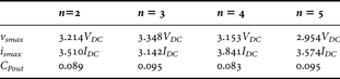
Obviously, the power output capability decreases and the drain voltage and current waveforms distort when the parameter n is even, and so it is not a good choice to construct a hybrid combining features of inverse class E and inverse class F. The reason is that theoretic inverse class F amplifier presents discontinuous drain current at the switching events which is incompatible with the ZCS conditions. Whereas incorporating traits of inverse class E and class F is a reasonable scheme. Table 2 shows that when n is odd the power output capability of the modified amplifier is slightly less than the classical class E and inverse class E mode. Especially when n = 3, the amplifier can be regarded as a realization of class F3/E mode, which is a hybrid of third-harmonic peaking class F [Reference Mihai19] and inverse class E. It displays lower peak drain voltage comparing to the classical class E and lower peak drain current comparing to the classical inverse class E.
Further analysis shows that the amplifier obtains some improvement when n is a non-integer near 3. The ideal drain voltage and current waveforms of the amplifier when n is swept from 2.9 to 3.1 are presented in Fig. 3. It demonstrates varying degrees of trade-off between the peak drain voltage and current when parameter n is set to different value. Figure 4 shows the power output capability of the amplifier versus parameter n. The maximum value of power output capability is 0.1022, which is obtained when n = 3.11. Finally, we let n = 3.1 and carry out an experiment based on the theoretical analysis above. Table 3 shows comparison of the proposed amplifier and class E and inverse class E.

Fig. 3. Ideal drain voltage and current waveforms of the amplifier when n is swept from 2.9 to 3.1.

Fig. 4. The power output capability of the amplifier versus parameter n.
Table 3. Comparison of the proposed amplifier and class E and inverse class E.

The proposed amplifier not only maintains the zero power loss switching operation, but also brings in some improvements as follows:
First, when DC supply voltage and load resistance are fixed, the modified amplifier obtains the highest output voltage V o and output power P o.
Second, the power output capability C Pout of the new configuration gets an increase of 4.1% comparing to the standard class E or inverse class E amplifier.
In addition, the new topology achieves more desirable drain voltage and current waveforms. The peak drain voltage for nominal class E operation is 3.562V DC, whereas for inverse class E amplifier the value is 2.862V DC. As a dual of class E topology, inverse class E amplifier has lower peak drain voltage; nevertheless, it brings high peak drain current whose value is 3.562I DC. When the parallel resonant tank is introduced to the invrese class E topology, the peak drain current decreases to 3.170I DC, and the peak drain voltage is 3.090V DC that is also much lower than the peak drain voltage vlaue of classical class E amplifier. This relaxes the design requirement on the transistor and is greatly beneficial to the device safety.
IV. SIMULATIONS AND EXPERIMENTS
To confirm the theoretical analysis and synthesis explained in Sections II and III, harmonic balance simulations have been carried out within Agilent Advanced Design Systems (ADS) suite. In these experiments, let n = 3.1 and then all the values of load network components can be calculated as introduced in Section III. Here the transistor used is MRF21010 manufactured by Freescale Corporation, whose physics-based Root model is available in the ADS library. Although the transistor MRF21010 is able to operate at 2GHz, its switching action deteriorates heavily because of the effects of parasitic components. In order to verify the practical performance of the proposed circuits, the power amplifier is built in low frequency (155 MHz), and then the device can be modeled as a switch approximately. From the above analysis the load network circuits can be fixed and then using the source-pull method we can obtain the optimal source impedance which is suitable for design input matching circuit.
Figure 5 shows the simulated drain voltage/current waveforms of the class E power amplifier proposed in this paper. The amplifier obtaining an output power 40 dBm at 155 MHz (DC voltage is 21 V and DC current is 1.12 A). It can be observed that the peak drain voltage and current are about 61 V and 3.5A, respectively. These values show the agreement with theoretical analysis. The waveforms in Fig. 5 are distorted lightly when compared to the idealized waveforms in Fig. 3. This is mainly due to the effects of some internal transistor parasitics and non-ideal switching action. There exist many factors that can degrade the amplifier performance. For example, the on resistance of a transistor can cause notable efficiency degradation because it consumes power during the on state. Whereas, at the microwave band, the effects of parasitic components such as output capacitance and lead inductance become notable. The distorted drain voltage/current waveforms which caused by parasitics will degrade the perormance and security of the PA. As a result, excellent switching device (such as GaN HEMT) should be utilizing when design frequency moves toward microwave operation. The schematic and photo of the experiment circuits are shown in Fig. 6. The simulation and measurement results are presented as follows.

Fig. 5. The simulated drain voltage/current waveforms (DC voltage is 21 V, output power is 10 W, and work frequency is 155 MHz).

Fig. 6. The schematic and photo of the test board.
Figure 7 depicts the output power, gain, drain efficiency, and power-added efficiency (PAE) of the simulations and the measurements versus DC supply voltage. It can be seen from Fig. 7 that the maximum simulated drain efficiency and PAE are 81.74 and 81.51%, and the maximum measured drain efficiency and PAE are 81.04 and 79.82%. Here, drain efficiency >75% for DC supply voltage ranges from 5 to 25 V is obtained. Obviously, the measured results agree well with the simulation. This implies that the output power can be well-controlled through direct variation of the DC supply voltage without unduly impairing efficiency.

Fig. 7. The output power, gain, drain efficiency, and PAE of the simulations and the measurements versus DC supply voltage (P in = 15 dBm, f = 155 MHz, V GS = 4.2 V).
Figure 8 shows the plot of output power, gain, drain efficiency, and PAE of the simulations and the measurements versus gate–source voltage. Because the used device Root model is not exactly the same with the practical transistor especially in the modeling of gate–source characteristics, the measured output power and drain efficiency are much lower than the simulated results when the gate–source bias voltage <2 V.

Fig. 8. The output power, gain, drain efficiency, and PAE of the simulations and the measurements versus gate–source voltage (P in = 15 dBm, f = 155 MHz, V DC = 21 V).
The output power, gain, drain efficiency, and PAE of the simulations and the measurements versus input power are illustrated in Fig. 9. Comparing measured results with simulated results, the excellent agreement was obtained. The output power rises with the increasing input power, and it goes into saturation area when the input power is high enough. Thus, the amplifier needs proper level of the input power to obtain the optimal performance.

Fig. 9. The output power, gain, drain efficiency, and PAE of the simulations and the measurements versus input power (V GS = 4.2 V, V DC = 21 V, f = 155 MHz).
The amplifier performance as a function of operating frequency is presented in Fig. 10. It can be seen that when the operating frequency is swept from 135 to165 MHz, the output power ranges from 39.58 to 40.31 dBm and the drain efficiency ranges from 71.03 to 78.24%. This amplifier can maintain its high efficiency and output power in the relative bandwidth about 20% (i.e. 30 MHz).

Fig. 10. The output power, gain, drain efficiency, and PAE of the simulations and the measurements versus operating frequency (V GS = 4.2 V, V DC = 21 V, P in = 15 dBm).
V. CONCLUSIONS
A modified inverse class E power amplifier with series tunable parallel resonant tank has been analyzed in this paper. The theoretical principles and design equations required to calculate the optimum circuit component values were given in detail. The proposed amplifier not only maintains 100% efficiency theoretically, but also brings in some improvements such as higher output power, power output capability, and further relaxes design requirements. The practical circuit implemented delivers 40.02 dBm output power at 155 MHz, and achieved PAE of 78.18%, drain efficiency of 78.42%, and 25.02 dB power gain when operated from a 21 V supply voltage. Experimental results show excellent agreement with simulations, which verifies the theoretical analysis. And the manufacture of this mode power amplifier with transmission-line load network at C-band will be the next work in future.
 Tao Cao received his bachelor's and master's degrees in electronic engineering from the University of Electronic Science and Technology of China (UESTC) in 2007 and 2010 separately. His research interests include RF/microwave analog circuit design and linearization techniques for high-efficiency power amplifiers.
 Songbai He received his bachelor's and master's degrees in electronic engineering from UESTC in 1995 and 1998 separately. He received his Ph.D. from UESTC in 2003. Now he is a professor of UESTC. His research interests include RF/MW circuits and systems, frequency synthesis, wireless communication, and non-linear dynamic systems.
 Fei You received his Ph.D. in electronic engineering from the UESTC in 2010. Now he is an assistant professor of UESTC. His research interests include high-efficiency power amplifiers design and its application in linear transmitters.


