I. INTRODUCTION
Diblock copolymers (BCPs) show phase separation on mesoscopic length scales and form ordered morphologies in both bulk and thin films resulting in nanostructured polymer surfaces (Benoit and Hadziioannou, Reference Benoit and Hadziioannou1988; Lazari and López-Quintela, Reference Lazzari and López-Quintela2003; Park et al., Reference Park, Yoon and Thomas2003; Segalman, Reference Segalman2005; Hamley, Reference Hamley2009; Kim et al., Reference Kim, Park and Hinsberg2010). In thin-film geometry, the morphologies are strongly influenced by film parameters and the ratio of the film thickness and the bulk domain spacing (Krausch and Magerle, Reference Krausch and Magerle2002; Knoll et al., Reference Knoll, Horvat, Lyakhova, Krausch, Sevink, Zvelindovsky and Magerle2002; Albert and Epps, Reference Albert and Epps2010). It is of high importance to understand these influences because laterally structured polymer surfaces may serve as template for the controlled assembly of nanoparticles (NPs) (Nandan et al., Reference Nandan, Kuila and Stamm2011).
In some BCP systems, for film thicknesses f well below d bulk (the “repeat distance”, which is controlled by the molar mass), standing morphologies were observed in appropriate molar ratios, while film thicknesses around and larger d bulk resulted in structures arranged parallel to the surface (Fasolka and Mayes, Reference Fasolka and Mayes2001; Krausch and Magerle, Reference Krausch and Magerle2002). In order to alter and/or improve the morphology – also in presence of different NPs (e.g., silica, gold, silver, magnetite) – often solvent vapour annealing (SVA) was applied (Jehnichen et al., Reference Jehnichen, Pospiech, Friedel, Korwitz, Berndt, Janke, Näther, Papadakis, Sepe and Perlich2010; Horechyy et al., Reference Horechyy, Nandan, Zafeiropoulos, Jehnichen, Göbel, Stamm and Pospiech2014).
The main goal of the present work is the creation of regularly ordered NP arrays by making use of the phase separation of the BCP in thin films as structural template for one-dimensional (1D) (standing lamellae) and two-dimensional (2D) (standing, hexagonally packed cylinders) morphologies, into which NPs can be incorporated selectively into one subphase.
The generation of such well-structured and stabile hybrid polymer/NP systems in thin films is demanding on both, chemistry and preparation. The first step is to find an appropriate block copolymer system with stable and reproducible morphology. Here, poly(n-pentyl methacrylate) – poly(methyl methacrylate) block copolymers (PPMA-b-PMMA) turned out to be well-suited (Jehnichen et al., Reference Jehnichen, Pospiech, Keska, Ptacek, Janke, Funari, Timmann and Papadakis2008, Reference Jehnichen, Pospiech, Ptacek, Eckstein, Friedel, Janke and Papadakis2009; Pospiech et al., Reference Pospiech, Werner (Ptacek), Jehnichen, Komber, Friedel, Reuter, Funari, Perlich and Voit2012). The specificity of this system is the all-methacrylic backbone allowing the easy removal of the BCP after templating. The synthesis of these BCP requires controlled polymerization methods. Sequential living anionic polymerization was proven as a suitable method (Keska et al., Reference Keska, Pospiech, Eckstein, Jehnichen, Ptacek, Häußler, Friedel, Janke and Voit2006; Werner et al., Reference Werner, Pospiech, Jehnichen, Eckstein, Komber, Friedel, Janke, Näther, Reuter, Voit, Taurino and Messori2011). Temperature-dependent small-angle X-ray scattering in transmission (T-SAXS) was used to gather information about the bulk structure of BCP after synthesis, such as the type and the characteristic parameters of the ordered morphology, e.g., lamellar or hexagonally packed cylinders (Jehnichen et al., Reference Jehnichen, Pospiech, Keska, Ptacek, Janke, Funari, Timmann and Papadakis2008; Werner et al., Reference Werner, Pospiech, Jehnichen, Eckstein, Komber, Friedel, Janke, Näther, Reuter, Voit, Taurino and Messori2011). In addition, thin-film preparation methods have to result in samples for advanced characterization with grazing-incidence small-angle X-ray scattering (GISAXS) experiments to investigate the presence of regular thin-film morphologies of these block copolymers. The method of choice for BCP films was always dip-coating under controlled conditions.
The present work aimed at investigating the effect of different annealing procedures [temperature and solvent vapour annealing, as reported in Sepe et al. (Reference Sepe, Cernoch, Stepanek, Hoppe and Papadakis2014) and Zhang et al. (Reference Zhang, Posselt, Smilgies, Perlich, Kyriakos, Jaksch and Papadakis2014)] on the improvement of the morphology.
Incorporation of NPs into the polymer matrix is probably the most important step of NP array preparation. NPs were either formed in situ in the BCP film by a sol–gel process according to (Fischer et al., Reference Fischer, Pospiech, Scheler, Navarro, Messori and Fabbri2008; Taurino, Reference Taurino2008) yielding silica NP, or, on the other hand, by adding pre-formed NPs (here: Au NPs) to the BCP solution before dip coating. Both techniques are regarded as possibility to insert NPs well directed to one phase of the block copolymer morphology. Figure 1 illustrates the goal and workflow of the present study.
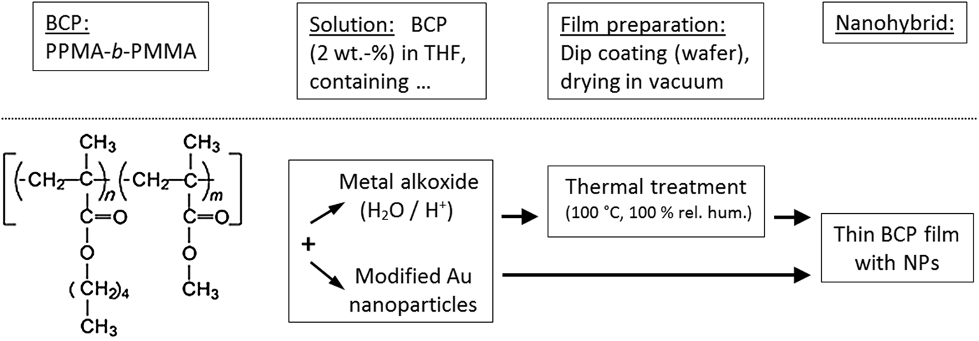
Figure 1. Schematic representation of the steps for achieving block copolymer/NP hybrids with PPMA-b-PMMA block copolymers in both applied preparation procedures.
Pre-characterizations of the materials and thin films were carried out using T-SAXS and X-ray reflectometry (XRR). Characterization of the thin-film samples as well as the structural changes after an online or offline sample annealing was realized in GISAXS experiments [for methodical details see, e.g., Müller-Buschbaum (Reference Müller-Buschbaum2003), Müller-Buschbaum (Reference Müller-Buschbaum2009), Jehnichen et al. (Reference Jehnichen, Friedel, Selinger, Korwitz, Wengenmayr, Berndt and Pospiech2013)] and atomic force microscopy (AFM) investigations. Moreover, the influence of the incorporated NPs onto the morphology of selected PPMA-b-PMMA was investigated.
II. EXPERIMENTAL
A. Sample preparation
1. Synthesis
a. The PPMA-b-PMMA BCPs
BCPs used in this study were synthesized by sequential living anionic polymerization in THF/LiCl at −78 °C using sec-butyl lithium/diphenyl ethylene as initiator as reported earlier (Keska et al., Reference Keska, Pospiech, Eckstein, Jehnichen, Ptacek, Häußler, Friedel, Janke and Voit2006; Werner et al., Reference Werner, Pospiech, Jehnichen, Eckstein, Komber, Friedel, Janke, Näther, Reuter, Voit, Taurino and Messori2011) aiming at narrow polydispersity (~1.1). The averaged molar masses M w and M n were determined by SEC yielding values relative to narrowly distributed PMMA standards. The samples employed in this work are listed in Table I.
Table I. BCPs PPMA-b-PMMA under investigation – chemical composition, molar masses, structure parameters of bulk morphology (T-SAXS) and thin films parameters from XRR and AFM (samples without NPs); all parameters are rounded.
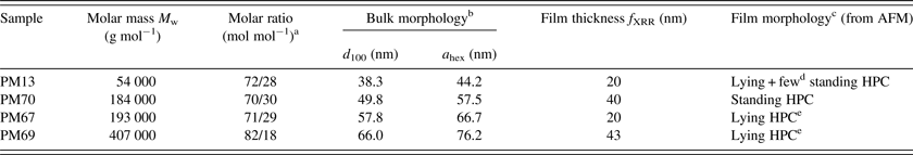
aAssignment according to Figure 1.
bAfter heating/cooling cycle to 200 °C; HPC, hexagonally packed cylinders.
cAfter dip-coating and subsequent drying at room temperature in vacuum.
dAmount of standing HPC is increased for higher content of Au NPs.
eFilm without silica NPs (before TEOS treatment).
b. The Au NPs (Au18)
NPs with an average core diameter of 2 nm (Figure 2) were prepared by the Brust–Schiffrin method (Brust et al., Reference Brust, Walker, Bethell, Schiffrin and Whyman1994) and were stabilized with dodecanethiol (Yee et al., Reference Yee, Jordan, Ulman, White, King, Rafailovich and Sokolov1999).

Figure 2. (Color online) (a) TEM image (magnification: 400 000 × , scale bar: 10 nm) and (b) NP size distribution of dodecanthiol-stabilized Au NPs (Au18) with mean core diameter of 2 nm.
2. Film preparation
Thin films of BCP were applied by dip-coating of Si wafers pre-cleaned by piranha solution at 80 °C for 0.5 h, followed by thoroughly rinsing with deionized water and drying with pressurized nitrogen.
Au NP containing films: pre-cleaned Si wafers were dip-coated by dilute BCP solutions (pure or with different contents of modified Au NPs) in tetrahydrofuran (THF). Subsequently, the wafers were dried at room temperature in a vacuum oven.
Off-line SVA was performed with THF (in saturated vapour for 1 h, followed by drying for 5 h in air, both at room temperature).
For silica NPs, an off-line procedure for the generation of silica inside the already prepared thin film was used. The films were prepared as described above by dip-coating. The in-film generation of silica NP (Fischer et al., Reference Fischer, Pospiech, Scheler, Navarro, Messori and Fabbri2008; Yuan et al., Reference Yuan, Xu, Walther, Bolisetty, Schumacher, Schmalz, Ballauf and Müller2008) was performed by treating the thin BCP films in three steps as follows: The films were stored in tetraethoxysilane (TEOS) saturated vapour over 24 h, than in H2O/HCl (9:1) saturated vapour for 10 h, and afterwards annealed for 2 h at 100 °C in vacuum.
B. X-ray scattering experiments and AFM
1. T-SAXS
T-SAXS was carried out at the Soft Condensed Matter Beamline BW4 (Roth et al., Reference Roth, Döhrmann, Dommach, Kuhlmann, Kröger, Gehrke, Walter, Schroer, Lengeler and Müller-Buschbaum2006; HASYLAB @ DESY Hamburg, λ BW4 = 0.138 nm) using a MarCCD 165 area detector (Marresearch Inc., USA). Oven experiments between room temperature and 200 °C were performed using heating/cooling rates of 3 K min−1.
2. XRR and GISAXS
XRR was performed using a diffractometer XRD T/T (GE Inspection Technologies Ahrensburg, Germany) in symmetric step-scan mode with Δ2Θ = 0.01° and t = 3 s (Cu Ka radiation) for pre-examination of few film parameters (e.g., film thickness).
GISAXS was carried out at the Beamline BW4 (Roth et al., Reference Roth, Döhrmann, Dommach, Kuhlmann, Kröger, Gehrke, Walter, Schroer, Lengeler and Müller-Buschbaum2006; HASYLAB @ DESY Hamburg, λ BW4 = 0.138 nm) using a MarCCD 165 area detector (Marresearch Inc., USA). The 2D-patterns with incidence angles α i = 0.03°–0.30°, i.e., close to the critical angles α c (polymer film, e.g., pure PMMA: α c,BCP ≈ 0.148°; substrate SiO x : α c,SiO x ≈ 0.20°), were accumulated with sufficiently high measuring time (typically 150 s) to find an optimal value α i so the lateral coherent scattering was most pronounced. This turned out to be the case for α i = 0.18° > α c,BCP.
3. Microscopic investigations
Transmission electron microscopy (TEM) investigations to measure the size of Au NPs were performed by means of a transmission electron microscope LIBRA 120 at IPF Dresden. At this, the NP dispersion was dropped on a TEM copper grid and afterwards dried in vacuum.
AFM measurements before and/or after film treatment and GISAXS experiments, respectively, were done with the scanning force microscope NanoScope IIIa-D3100 (Digital Instruments) in tapping mode. The mean lateral distances L 0 from the power spectral distribution (PSD) obtained by Fast Fourier Transform (FFT) of the AFM image were calculated using the related AFM software.
III. RESULTS AND DISCUSSION
A. Bulk behaviour
All PPMA-b-PMMA BCP samples employed in the study showed morphologies with hexagonally packed cylinders. Three of them had a molar ratio PPMA/PMMA of 70/30 mol mol−1, for which the hexagonal morphology is expected (Table I), but also the very asymmetric sample PM69 with a molar ratio of 82/18 mol mol−1 displayed this morphology. Figures 3(a)–3(d) illustrate the scattering curves of the bulk material after a complete heating/cooling cycle starting from the as-synthesized state. Based on the position of the first scattering maximum, q 1, and the known ratios of the next allowed reflections q n/q 1 of the hexagonally packed cylinder morphology (HPC) (i.e. 1: √3: √4: √7: √9: …), the expected positions of the higher order reflections were calculated [see Figures 3(a)–3(d)]. This way, an HPC morphology could be identified for all samples. The corresponding morphology parameters, namely the lattice spacings (d 100) and corresponding cylinder–cylinder distances, a hex (unit-cell parameter of HCP), are given in Table I.

Figure 3. (Color online) Lorentz-corrected SAXS curves of corresponding BCP bulk material with hexagonal packed cylinder morphologies [with Miller indexing of the first reflections (hk0)]. (a) PM13, (b) PM70, (c) PM67, and (d) PM69.
B. Thin films
1. XRR and AFM
For determination of the film thickness, pre-evaluation of the film roughness and direct visualization of the thin-film morphology XRR and AFM investigations were performed prior to GISAXS experiments. As-prepared films (film thicknesses f XRR ranging from 20 to 43 nm) show distinct Kiessig interferences, low roughness (typical rms-roughnesses 0.7–0.8 nm) and good preparation reproducibility. The AFM images give a direct impression of the morphology in the topmost layer of the thin film (see, e.g., Figure 5). Film parameters obtained by XRR and AFM are summarized in Table I.
2. GISAXS results and film treatment
a. BCP films with Au NPs
In a first sample series, the results of film preparation from the appropriately diluted BCP/Au NP solution with different amount of NPs were compared. The Au NPs (Au18 with an average core diameter of 2 nm) are surface modified with dodecane thiol. The alkyl rest is hydrophobic and the preferential interaction with the pentyl methacrylate block should direct the NPs into the PPMA phase. The GISAXS results for PM13 films with low and medium content of Au18 NPs in comparison with the pure BCP film and one test of offline SVA (BCP film with 5 wt.% Au NPs) are given in Figures 4(a)–4(d). It shows the influence of the amount of Au NP and SVA, respectively, on the laterally ordered morphology. Besides scattering experiments, AFM measurements were carried out and evaluated by means of PSD [Figures 5(a)–5(d)].

Figure 4. (Color online) 20 nm films of sample PM13/Au18 vs. concentration of NPs [(a–d): 0, 1, 5, and 5 wt.%] and influence of SVA with THF [(a–c) as spin-coated, (d) vapour-annealed]. GISAXS pattern, scattering intensity plot (in miscolour) log(I) vs. q z , q y (q z range: approx. 0.08–0.78 nm−1, q y range: approx. −0.40–0.40 nm−1, mesh size Δq = 0.1 nm−1).

Figure 5. (Color online) AFM results from 20 nm films of sample PM13/Au18 vs. concentration of NPs [(a–c): 0, 1, and 5 wt.%; as spin-coated]. AFM phase contrast images (pattern size 2 × 2 µm2, scale 3°); (d) PSD of FFT image of AFM image (a) (L 0 is the result from reading of the peak position).
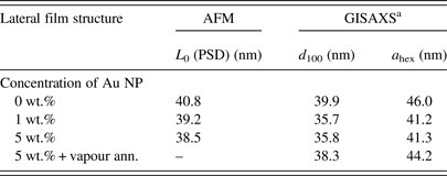
In comparison to the pure BCP film morphology, the lateral distance of cylinders is reduced with increasing content of NPs in the case of the small Au NPs (core diameter of 2 nm) used in the present study. This behaviour differs from the case of significantly larger Au NPs (average core diameter of ~10 nm) (He, Reference He2014), where it was found that the required space of these larger NPs perturbs the morphology. However, SVA of the sample with 5 wt.% small Au NPs enlarges the lateral distance. From this change in the repeat distances we conclude that the Au NPs after SVA are located either in the PMMA domain or at the interface between the PPMA and the PMMA domains. The latter scenario can be ruled out due to the fact that the repeat distance shrinks when the NPs are at the interface because the interfacial tension is reduced (He, Reference He2014). The third possibility – equal distribution of Au NPs within the film – can be excluded because of the strong enhancement of the reflections when Au NPs are added (Figure 6) in comparison to the pure BCP film.

Figure 6. (Color online) GISAXS results from 20 nm films of sample PM13/Au18 vs. concentration of NPs [(1–3): 0, 1, and 5 wt.%) and influence of SVA with THF (4) for film with 5 wt.% Au NPs]. Out-of-plane curves from the GISAXS patterns [Figures 4(a)–4(d)], taken at q z = q Yoneda,BCP.
The position of the lateral correlation peak (Table II) does not scale with the amount of NPs. From the AFM image [Figures 5(a)–5(c)], it can be concluded that lying parallel cylinders in the BCP film without NPs switch to a mix of both lying and standing (perpendicular) cylinders and an amount of randomly oriented ones when Au NPs were incorporated. The amount of standing cylinders increased with the concentration of Au NPs.
Table II. Hybrid thin films of BCP PM13 with Au18 NPs – thin-film parameters and effect of SVA (L 0 from AFM, GISAXS d values found at α i = 0.20°; all parameters are rounded).

aGISAXS shows often only one broad lateral correlation peak (set as d 100). a hex, unit-cell parameter, derived from d 100; problematical in case of mixed arrangements of lying and standing cylinders (Lee et al., Reference Lee, Park, Yoon, Park, Kim, Kim, Chang and Ree2005).
The orientational switch of the nanodomains can be explained by the altered interaction of the BPC with the substrate because of modified Au NPs. In the pure BCP, the hydrophilic PMMA block tends to wet the substrate partially, resulting in lying cylinders. When Au NPs are present and assemble selectively in the PMMA domains, the PMMA cylinders become more hydrophobic, thus they reduce their contact with the substrate, which result in standing cylinders.
An additional SVA with the non-specific solvent THF of the BCP film containing 5 wt.% Au NPs resulted in a lateral improvement of the thin-film morphology (i.e., in sharper reflections) as well as along the film normal, as seen from the enhanced Bragg rods in the GISAXS pattern [compare Figures 4(c) and 4(d)]. The reason is probably that THF is a non-selective, good solvent for both blocks which enhance the polymer mobility in the swollen state which allow structural rearrangements. On the other side, a generation of thin layers of Au NPs near the film surface or near the substrate surface cannot be excluded absolutely. The increased background of the out-of-plane curves (4) in Figure 6 (BCP film with 5 wt.% Au NPs after SVA treatment) could follow from such NP enrichments.
b. BCP films with silica NPs
In a second sample series, it was investigated whether silica NPs can be generated by TEOS treatment of a previously prepared nano-patterned BCP thin film. The treatment is based on the interaction of the silica precursor TEOS with the film surface over different treatment steps. The actual content of silica cannot be determined after such a procedure. The results of the treatment steps were monitored by offline GISAXS measurements [as an example, see Figures 7(a)–7(d)].

Figure 7. (Color online) GISAXS patterns of 40 nm thick films of sample PM70 after offline TEOS treatment (generation of SiO2 NPs). (a) as coated, (b) after treatment with TEOS vapour, (c) after treatment with H2O/HCl vapour, (d) after annealing at 100 °C in vacuum. Scattering intensity plot (in miscolour) log(I) vs. q z ,q y (q z range: approx. 0.12–0.75 nm−1, q y range: approx. −0.36–0.36 nm−1, mesh size Δq = 0.1 nm−1). Additionally in (a), an AFM phase contrast pattern is shown (pattern size 2 × 2 µm2, scale 3°).
For the BCPs PM70, PM67, and PM69, the out-of-plane intensity profiles of the corresponding GISAXS patterns after each treatment step are compared in Figures 8(a)–8(c). In the nanohybrids under investigation, the type of morphology remains the same as in the pure BCP. For all treatment steps shown in Figures 7 and 8, a lateral arrangement of standing cylinders with hexagonal packing over a certain correlation length is found. However, there are differences when comparing the quality of lateral correlation of the cylinders in three different BCPs. PM67 with a film thickness of only 20 nm and the largest ratio a hex/f (i.e., ratio of domain size to film thickness) shows the best ordered HPC morphology because of lower peak widths and presence of higher order reflections. Moreover, from the enhancement of the correlation peak intensity during the TEOS treatment, we conclude that silica particles are selectively generated in the PMMA cylinders. In contrast, the thin films of both PM70 and PM69 (film thickness ~40 nm) feature a significantly lower quality of HCP morphologies. Moreover, contrary to PM67, the intensity of the reflection decreases during the TEOS treatment. From this, it can be concluded that the generation of silica takes place in both, the PMMA and the PPMA domains. After the in situ generation of silica NPs only weak changes of lateral distances are found, such as an increase of about 2.2 nm (PM69) or a reduction of about 2.5 nm (PM70), or no change (PM67) (compare Table III).

Figure 8. (Color online) Thin films of samples (a) PM70, (b) PM67, and (c) PM69: out-of-plane curves from GISAXS patterns at q z = q Yoneda,BCP after offline TEOS treatment [(1) as coated, (2) after treatment with TEOS vapour, (3) after treatment with H2O/HCl vapour, (4) annealed at 100 °C in vacuum], curves are shifted vertically for clarity. Corresponding 2D GISAXS patterns are given in Figures 7(a)–7(d) at the example of sample PM70.
Table III. Silica generation in PPMA-b-PMMA films – thin-film parameters after treatment (GISAXS: d values found at α i = 0.20°; all parameters are rounded).
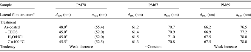
aFollowing the morphology found by AFM as HPC, regardless of details in lateral intensity distribution of GISAXS (often only one broad peak, which was used to determine d 100). a hex, unit-cell parameter, derived from lateral correlation peak.
bBroad reflection.
It has previously been shown by us that functionalization of the PMMA blocks by –OH end groups resulted in BCP that worked well as a template for the formation of silica NPs by TEOS treatment (Werner et al., Reference Werner, Pospiech, Jehnichen, Eckstein, Komber, Friedel, Janke, Näther, Reuter, Voit, Taurino and Messori2011). From the GISAXS experiments (Figures 7 and 8), it can be concluded that the off-line silica generation caused also an enhancement of the diffuse scattering because of the increased background of the out-of-plane curves (having the highest values after the last treatment step). Moreover, a defined amount of randomly oriented cylinders cannot be excluded.
IV. CONCLUSION AND OUTLOOK
In addition to the structures expected from the bulk morphologies, thin-film structures of BCP are characterized by the geometric confinement resulting in orientation effects, which depend on the ratio between the film thickness and the bulk domain spacing. The present investigation demonstrates that two routes to prepare nano-patterned thin BCP thin films based on PPMA-b-PMMA with NPs allow us to obtain thin films in a range of film thicknesses having low roughness and good reproducibility. These preparation routes are dip-coating of Si wafers with dilute solutions of BCP and NPs and off-line treatment of previously prepared, pure BCP films with vapour containing a precursor of the final NPs. In the nanohybrids under investigation (PPMA-b-PMMA BCPs with Au and silica NPs), the type of morphology remains similar to the one in the pure BCP film. The dimensions of the lateral film morphology depend weakly on type and amount of incorporated NPs as well as on the molar mass and the composition of the BCP. For the examined sample systems, it can be stated that silica NPs can lead to both an increase and a decrease of the lateral distance of the PMMA cylinders. On the other hand, metallic NPs often lead to a decrease of the domain spacing (confirmed here for the case of small Au NPs). This result is in accordance with the result found by Horechyy et al. (Reference Horechyy, Nandan, Zafeiropoulos, Jehnichen, Göbel, Stamm and Pospiech2014). In the present system, an enrichment of NPs in the surface region is not observed, but cannot be excluded either because of the presence of diffuse scattering in case of generated silica NPs. More detailed X-ray scattering investigations, especially for off-line generation of silica NPs, have to be performed to clarify the effects of constrained dimensions onto the morphology variation in thin films with altered film thickness, but still smaller than the domain spacings.
ACKNOWLEDGMENTS
The authors gratefully acknowledge financial support by and participation in EU NoE “NANOFUN-POLY”. The authors thank HASYLAB @ DESY Hamburg (now: DESY Photon Science) for providing beamtime and offering excellent equipment. Moreover, the authors thank all not-named colleagues of the IPF participating in synthesis and characterization of the studied polymers. Special thanks go to Kathrin Eckstein for anionic polymerization and Andreas Korwitz for excellent assistance during the GISAXS experiments, especially during the TEOS treatment.