


Introduction
Radiofrequency and microwave enjoy numerous applications in various fields such as point-to-point communication, wireless communication, military applications, and radar communication [Reference Qin and Brosseau1]. The intense use of electromagnetic (EM) wave in various applications gives rise to EM pollution in the environment. In our contemporary society, EM pollution causes many diseases, e.g. headaches, sleeping disorders, trepidation, etc., and has been ranked as the fourth source of pollution by the World Health Organization [Reference Seyhan2, Reference Ionut3]. EM pollution also deteriorates the functioning and durability of electronic equipment. Therefore, this pollution has become a serious worldwide concern and it can be reduced by either shield mechanism or absorption mechanism. Compared with EM shielding material, microwave-absorbing materials (MAM) are powerful alternatives to eliminate pollution due to their effectiveness in dissipating microwave energy without any secondary pollution. In general, MAM and microwave-absorbing structures should satisfy general requirements that are enlisted as follows: it should (i) minimize the reflection of EM waves at the air to absorber interface; (ii) have strong absorption of EM waves; (iii) have broad bandwidth and angular response; (iv) have low weight and thickness [Reference Al-Zoubi and Naseem4]. Unfortunately, meeting these competing requirements simultaneously is a challenging task. To meet these objectives and enhance the efficiency of MAM, tedious and extensive techniques have been suggested [Reference Al-Zoubi and Naseem4]. These techniques can be categorized into two main categories: material and geometry based. In the material-based technique, the microwave properties of the material complex permittivity (ɛ) and permeability (µ) are tailored in a manner to increase electrical and magnetic losses of the material. In the geometry approach, the MAM is constructed in a certain structure with particular geometry and dimensions that reduce the reflection and enhance confinement and absorption of the EM waves inside the structure. Different types of materials used as MAM, such as carbon, metal and metal particles, conducting polymers, polyaniline conducting polymer, tubules and filaments, and recently composite of nano-materials, have been discussed in the literature [Reference Melvin, Ni, Suzuki and Natsuki5–Reference McNally and Pötschke11].
Nowadays, chemical-based materials and ferrite are used to fabricate microwave absorber (MA). The fabrication procedure is costly and the materials are not bio-degradable. Also, they are not environment-friendly due to their toxic emission under high temperature which can pose a health risk to direct contact personnel [Reference Smythe, Casserly and Arakaki12]. Due to the high cost of the ferrite materials, their transportation, and their large densities, we are forced to quest for alternative materials. The basic element that is used very often in the absorber is carbon. Being a semiconductor material, carbon allows a small amount of charge to flow through it and has favorable electrical characteristics. In order to fabricate low-cost and eco-friendly absorber, agricultural residues having high carbon content have proved to be a useful alternative material in the microwave communication field. MAM using agricultural residues, such as rice husk, rice straw, oil palm empty fruit bunch, sugar-cane bagasse, coconut coir, and coconut shell powder, has been studied and remarkable absorption performance has been reported [Reference Nornikman, Soh, Azremi, Wee and Malek13–Reference Liyana, Malek, Nornikman, Mohd Affendi, Mohamed, Saudin and Ali21]. The carbon content found in rice husk, oil palm empty fruit bunch, sugar-cane bagasse, and coconut shell charcoal is 35.77, 40.5, 17.89, and 83%, respectively [Reference Nornikman, Malek, Soh, Abdullah Al-Hadi, Wee and Hasnain22–Reference Sai, Ahmed and Krishnaiah25].
The carbon content present in the dried banana leaves is 43.5% [Reference Zulkifli, Wee, Mahrom, Yew, Lee, Ibrahim and Am Phan26] more than the reported agricultural residues. Single-layer MA have numerous applications in military and civil industries due to expedient and cost-effective fabrication. The aim of this investigation is a first time attempt to design a single-layer flat-shaped MA using dried banana leaves and study the dielectric properties as well as microwave absorption performance. In this investigation, single-layer MA structure has been comprised of a lossy absorbing layer and a PEC (perfect electrical conductor) as a reflective layer, and the structure is usually known as Dällenbach layer [Reference Dallenbach and Kleinsteuber27]. A 99.9% pure copper plate of 0.21 mm thickness has been used as a PEC. In this study, we have designed the whole research work in five sections: (i) Theoretical aspects, (ii) Sample fabrication method, (iii) Measurement method, (iv) Simulation strategy, and (v) Result and analysis. Section “Theoretical aspects” introduces the basic theory on the master factor of microwave absorption. In section “Sample fabrication method”, the fabrication procedure of a single-layer absorber with different thicknesses has been discussed. In section “Measurement method”, particle size, the thickness of the particle board, and dielectric properties of the dried banana leaves in the form of powder as well as particle boards have been measured using an optical microscope, digital caliper, and open-ended coaxial probe (OCP) method, respectively. In section “Simulation strategy”, the simulation strategy has been described. In section “Result and analysis”, the absorption performance of a single-layer absorber has been analyzed in terms of experimental and simulative aspects. Also, the impact of thickness on microwave absorption efficiency has been explored in this section. Eventually, the article has been concluded with a quest for another exploration.
Theoretical aspects
MAM have to achieve general requirements which are difficult to accomplish simultaneously. While designing a MA structure, the aim is to accomplish two targets: (i) reducing reflection and (ii) increasing absorption over broadband frequency. Reducing the reflection can be met by wave impedance matching and increasing the absorption can be met by controlling the dielectric properties of the materials.
When an EM wave penetrates and propagates through the material, the experience is divided into three mechanisms which are a reflection of the incoming wave, absorption of the wave as it passes through the thickness of the material, and transmission of the wave. The absorption characteristics of the material rely on its dielectric properties such as complex permittivity, loss tangent, and conductivity [Reference Vinoy and Jha28]. The complex permittivity is a dominating factor which determines how the EM field interacts with the molecular structure of the material. When an EM field is applied across a dielectric material, translational motion of electrons or ions is induced by the internal field, thus it rotates the dipole and dipoles are aligned accordingly and the material is said to be polarized and the polarization mechanism is known dipolar polarization. Inertial, elastic, and frictional forces impede this induced motion as well as the realignment of dipoles and cause energy loss which leads to heat dissipation. Another polarization mechanism which also plays a role in absorption mechanism is conduction mechanism. In this mechanism, any mobile charge carriers (electrons, ions, etc.) move back and forth through the material under the influence of the electric field, creating an electric current. These induced currents will cause heat generation in the materials due to any electrical resistance caused by the collisions of charged species with neighboring molecules or atoms. The complex permittivity is a frequency-dependent parameter which can be expressed with the following expression [Reference Nath29]:

where ɛ ′ is known as the dielectric constant which characterizes the material's ability to store and release EM energy, ɛ ′′ is the loss factor or dissipative factor which corresponds to the material's ability to absorb or attenuate EM energy to create thermal energy.
There is another related factor to microwave absorption namely loss tangent, commonly used to indicate the efficiency of conversion of microwave energy into thermal energy within the dielectrics and is given in (2) [Reference Nath29]:

It is defined as the ratio of the energy dissipated to the energy stored in the dielectric material. The more energy that is dissipated into the material, the less energy will penetrate into the dielectric material. This dissipated energy is converted into heat. The main principle of absorption mechanism is heat dissipation. Absorption is a necessary parameter in determining the optimum condition when designing an MA. An optimal absorber should provide 100% absorption of the entering signal. The power loss in terms of heat generation due to the electrical component of the EM wave can be further explained by the following equation [Reference Tsubaki, Azuma, Fujii, Singh, Thallada, Wada, Bhaskar, Pandey, Venkata Mohan, Lee and Khanal30, Reference Rosa, Veronesi and Leonelli31]:

where P represents the power density in the material (W/m3), σ is the electrical conductivity (S/m), ω = 2πf(Hz); f is the frequency of the incident microwaves, ɛ′′ is the dielectric loss factor, ɛ 0 is the permittivity of free space, E represents the electric field strength (V/m).
Conductivity is another factor which contributes to the conductive loss and it is the main parameter in determining the loss factor. The conductivity of the material is given in (4) [Reference Green and Chen32] Fig. 1:

where ɛ 0 = 8.854 × 10⁻¹² F/m.

Fig. 1. Possible paths of the incident electromagnetic wave in a material.
The components of the incident power distribution inside the material where Pi, Pr , Pa, and Pt are incident, reflected, absorbed, and transmitted power, respectively, are expresses as:

Equation (6) shows the expression of return loss:

Absorption profile AR(ω) of the material can be determined as [Reference Nath29]:

where S 11 is the reflected signal and S 21 is the transmitted signal.
In the context of the measurement setup, we measured the S 11 parameter and the ground plane (PEC) allows minimal transmission. From both the point of view, transmission loss (S 21 ~ 0) can be neglected. Therefore, (8) is the reduced form of (7) and it validates the measurement setup:

Within the MAM, the microwave energy decays exponentially with distance x by a factor e −αxwhere attenuation constant (α) is given by [Reference Rubrice, Castel, Himdi and Parneix33]:

where ω = 2πf and f is the frequency of microwave, C is the speed of light in vacuum, μ ′ is the relative permeability of the material (μ ′ = 1), ɛ′ and tan δ are the EM parameters of the material. A is the adjustment factor (A = 8.68/100 dB/Np) to convert α in dB/cm. The above expression indicates that the attenuation of microwave power for a dielectric absorber depends on ɛ ′ and tan δ. From (2), it can be concluded that the higher the imaginary part of the complex permittivity, the bigger the loss tangent and the better the wave absorption effect.
When an EM wave penetrates into the material and propagates through the material, the power of the wave drops to 37% of its initial value at a certain distance from the surface. The distance is known as skin depth and it is given by [Reference Yah, Rahim, Lee, Wee and Zainal34]:

Sample fabrication method
Figure 2 illustrates the flow of work for developing the flat-shaped particle board. The structure of the work plan consists of five phases, i.e. collection, grinding, measurement of dielectric properties, the addition of resin and hardener agent, and simulative analysis. Shape plays a significant role in the absorption performance of a good MA. The frequency range considered in this investigation is 1–20 GHz. In this research work, three particle boards of various thicknesses are fabricated and the dimension of the boards is given in Table 1. Banana leaves are taken and dried for a week under the sun. They are blended using a grinder to make a fine microscopic powder. Figure 3 shows the dried banana leaves in microscopic powder form.
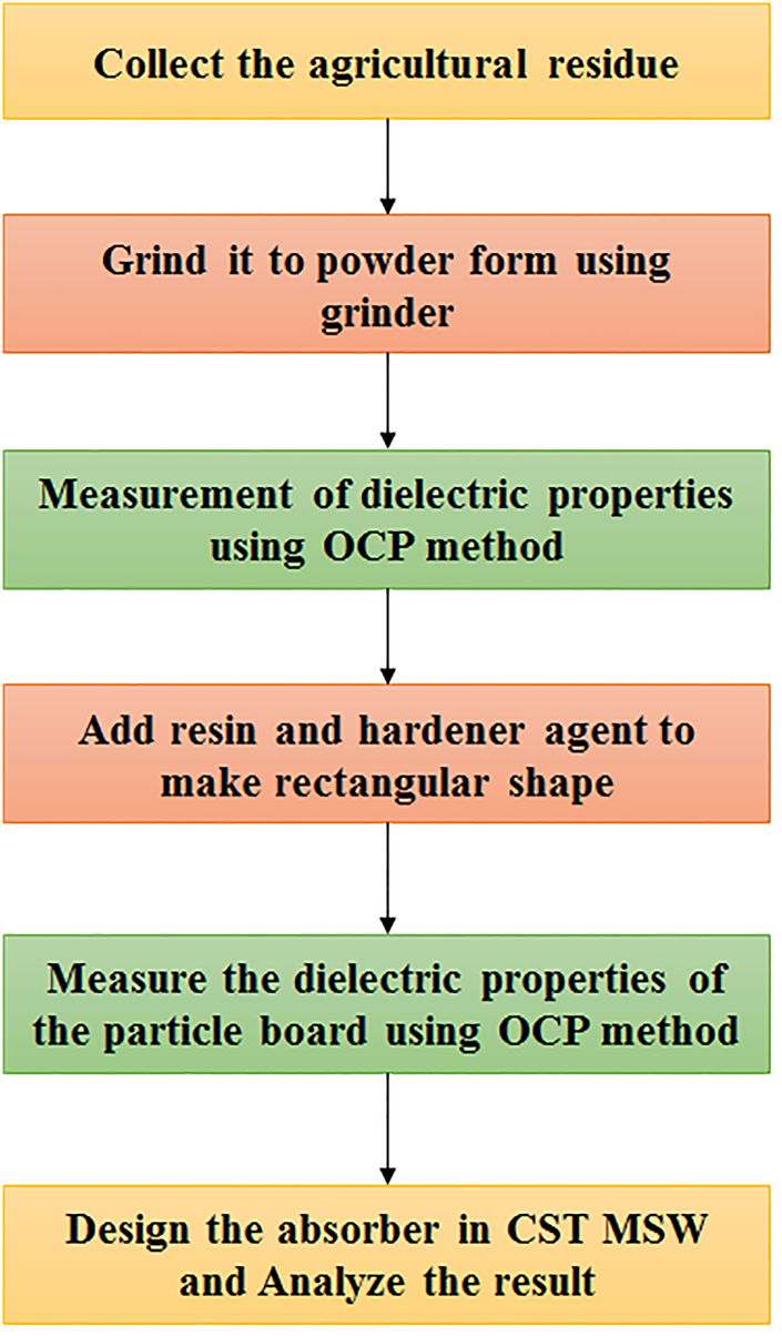
Fig. 2. Steps of developing banana leaves-based rectangular-shaped microwave absorber.

Fig. 3. Dried banana leaves in powder form.
Table 1. Sample preparation for microwave property measurement and mould sample dimensions

To fabricate a particle board, different types of resin and hardener can be used. Urea formaldehyde, phenol formaldehyde, and polyurethane were used in some studies [Reference Nornikman, Soh, Azremi, Wee and Malek13, Reference Liyana, Malek, Nornikman, Mohd Affendi, Mohamed, Saudin and Ali21]. But these resins are not eco-friendly and are human health hazards. In this work, polyester resin, methyl ethyl ketone peroxide, and cobalt have been used as a binding agent, hardening agent, and an accelerator for the fabrication of the particle board. These compounds are also USDA approved for food container production [35]. Hence, they are not malign agents for either human health or the environment. Resin with a hardening agent binds the material, and the layers of the two constituents impart strength to it and protect it from abrasion. Figure 4 shows the particle board fabricated by banana leaves powder.

Fig. 4. Banana leaves particle board.
Measurement method
Particle size measurement
Figure 5 shows the microscopic view of the banana powder particles with 20× optical zoom. The size of the particles is not uniform as it is crushed using a grinder. The size of the particles is in the micrometer range, i.e. from 100 to 500 μm. The size of the grain plays an important role in microwave absorption performance. Small size grain means a higher surface area, more surface atoms, multiple reflections, and thus larger dielectric constant or/and dielectric loss. These lead to the interfacial polarization and multiple scatter which is useful to enhance the microwave absorption performance [Reference Idris, Hashim, Abbas, Ismail, Nazlan and Ibrahim36].

Fig. 5. Microscopic view of banana leaves powder.
Thickness measurement
The thickness of the sample has an important role in microwave absorption performance. The microwave absorption performance is analyzed by varying the thickness of the rectangular sample. Hence, it becomes very much necessary to measure the sample's thickness. In this study, the digital caliper is used to measure the thickness of the samples. Figure 6 shows the thickness measurement setup using a digital caliper and the measured value is given in Table 1.

Fig. 6. Thickness measurement using a digital caliper: (a) samples and (b) PEC.
Hardware measurement
Different measurement methods such as OCP method, transmission line technique, free space measurement technique, and resonant cavity technique can be used to determine dielectric properties [37]. In this investigation, the OCP method has been used to measure the dielectric properties of the banana leave powder and the particle board. The sample is placed in close contact with the probe or the probe is pressed against a material under test or immersed into the liquid sample. Therefore, the dielectric properties are calculated from the phase and amplitude of the reflected signal using software embedded in the vector network analyzer (VNA). Before measurement, the dielectric probe is first calibrated with the help of air, a metallic shorting block, and water [Reference Pattanayak, Bachhar and Sahoo38].
In this investigation, R&S ZNB-20 VNA and DAK (Dielectric Assessment Kit) are used to measure the dielectric properties of the banana leaves powder as shown in Fig. 7. The measurement set up is shown in Fig. 8.

Fig. 7. Dielectric parameter measurement of dried banana leaves to powder using a dielectric probe technique.

Fig. 8. Measurement setup.
Simulation strategy
The single-layer absorber has been designed in CST Microwave Studio (CST MWS) 2019 3D EM simulation software for high-frequency components. The dimension taken for the simulation is given in Table 1. The material is dispersive and that is why the absorber has been designed and simulated in CST MWS using the 1000 value of dielectric constant and loss tangent at 1000 frequency point in the range from 1 to 20 GHz obtained from the measurement. The CST simulations are carried out under plane wave incidence along with open-add space boundary conditions.
Result and analyses
Dielectric properties of dried banana leaves powder and particle board
At the foremost, the frequency-dependent EM parameters of the dried banana leaves have been measured using DAK-3.5 probe, P/N: SM DAK 040 CA as shown in Fig. 9. The average value of the dielectric properties has been computed using the equation given below:

where N is the floating point of frequency.

Fig. 9. Dielectric properties of dried banana leaves, (a) dielectric constant, (b) loss factor, (c) loss tangent, and (d) conductivity.
In our investigation, N has been considered as 1000 to obtain the dielectric behavior precisely in the entire frequency range from 1 to 20 GHz. The average dielectric constant, loss factor, loss tangent, and conductivity are 1.47, 0.078, 0.041, and 0.053 S/m, respectively, in the entire frequency range.
The measurement of dielectric properties of samples A 1, A 2, and A 3 is also performed as given in Fig. 10. The result shows the better dielectric properties of a single-layer MA structure in comparison with dried banana leaves powder. An increase in density leads to a high dielectric constant [Reference Mezan, Malek, Jusoh, Abdullah and Affendi17] which causes the decrease of wave velocity [Reference Nornikman, Soh, Azremi, Wee and Malek13]. Resin with a hardener agent and accelerator binds the material and the layers of two constituents by reducing the air gap between consecutive particles. Therefore, the dipolar polarization and density are increased and the effect points toward the increase in the dielectric constant of the single-layer MA structure. The result also shows that the dielectric properties vary with change in the thickness of the absorber as given in Table 2. The loss factor and loss tangent are little fluctuating in nature as observed in earlier studies [Reference Farhany, Malek, Nornikman, Affendi, Mohamed, Saudin and Ali39]. This is probably due to the free electron (conduction current) and dipolar polarization within the compact design. However, the decrease in static permittivity (ɛ′) with an increase in frequency for each sample indicates the natural phenomenon because of orientation polarization. An increase in the thickness increases the dielectric constant which is not the same for sample A 3. It may be because of an increase in the flow of conduction current due to larger surface area. The result shows that sample A 2 exhibits the better dielectric characteristics among three samples and it points toward the better absorption of microwave power comparatively than others.

Fig. 10. Dielectric properties of a single-layer absorber for 8, 16, and 32 mm thickness, respectively, (a) dielectric constant, (b) loss factor, (c) loss tangent, and (d) conductivity.
Table 2. Comparative study of average dielectric properties and skin depth of the single-layer absorber using dried banana leaves

The skin depth is calculated using (10) and is plotted in Fig. 11. The skin depth analysis depicts that the microwave loses 37% of its initial power at 1 GHz frequency for every sample and it occurs at 0.86, 0.37, and 0.49 mm distance from the surface of the samples 1, 2, and 3, respectively. It is very much evident from this investigation that the skin depth varies with frequency, loss factor, and dielectric constant of the material.

Fig. 11. Skin depth of a single-layer absorber for 8, 16, and 32 mm thickness.
Microwave absorption performance and absorption mechanism
When the EM waves transverse through the medium, the amplitude of the wave experiences an exponential decay with respect to the distance (x) by a factor e −αx(E = E m × e −αx), where α is the attenuation constant of the material and is a function of loss tangent and is expressed in (9). The effect of the various parameters for the absorption (A) of EM wave incident is given by [Reference Tirkey and Gupta40]:

where E and H are the electric and magnetic field strength of the incident wave, respectively, σ is the conductivity of the material, ɛ 0 and μ 0 are the permittivity and permeability of the free space, respectively, ɛr and μr are the relative permittivity and permeability of the material.
As the paper concerns with a dielectric material, the above expression can be rewritten as:

Therefore, the absorption of EM wave incident on the absorbing surface is dependent on the attenuation constant of the material which is a function of loss tangent as well as the imaginary part of permittivity. Therefore, it can be inferred that the bigger the imaginary part of complex permittivity, the better the wave absorption effect [Reference Huo, Wang and Yu41].
The maximum return loss point cannot depict the entire performance of an absorber as it barely interprets at a particular frequency or in the limited frequency range. Hence to obtain the overall scenario of the absorption performance of an absorber, one needs to calculate the average return loss profile. The average reflectivity is computed using (11), where N = 1000. The requirement for acceptable performance of an MA is to have return loss better than −10 dB (90%) [Reference Salleh, Yahya, Awang, Muhamad, Mozi and Yaacob18, Reference Nornikman, Malek, Soh, Abdullah Al-Hadi, Wee and Hasnain22]. The microwave absorption performance in terms of reflectivity is analyzed by reflectivity (S 11) measurement and simulative analysis.
The experimental analyses are the validation of simulative analyses of three different samples. The OCP method is used to extract the S 11 parameter of the samples shown in Fig. 8 and (8) is used to compute the microwave absorption. Both the results show that the maximum reflectivity occurs at very low frequency for every sample as shown in Fig. 12 and Table 3. Skin depth analysis also indicates the same, i.e. the power of the wave drops to 37% of its initial power for each sample at 1 GHz frequency. As the single-layer MA structure is homogeneous in nature, the absorption mechanism is influenced by the dipolar polarizability of the absorbing layer of the absorber. At very low frequency, the dipoles of the absorber are free to rotate and dissipate the energy in terms of heat which indicates the imaginary part of the complex permittivity. As the frequency increases, the material's net polarization drops as each polarization mechanism ceases to contribute, and hence the decrease in the imaginary part of complex permittivity as well as dielectric constant. The outcome is the decrease in absorption performance with the increase in frequency as observed in Fig. 12. The maximum return loss profile and average return loss profile of samples A 1, A 2, and A 3 have been illustrated in Tables 3 and 4. From the dielectric properties measurement, the result shows A 2 (ɛ′′) > A 3 (ɛ′′) > A 1 (ɛ′′) and the same trend has been observed in the absorption performance of the samples.

Fig. 12. Comparative analyses of return loss profile of a single-layer MA for the samples with various thicknesses: (a) A 1, (b) A 2, and (c) A 3.
Table 3. Maximum absorption rate of the single-layer absorber for 8, 16, and 32 mm thickness at the resonant frequency

Table 4. Average absorption rate in terms of the return loss of the single-layer absorber for 8, 16, and 32 mm thickness over 1–20 GHz frequency range

The simulative analyses of return loss profile differ slightly from experimental validation. The average error has been also given in Table 4 and it is approximately 25%, quite significant and also observed in earlier studies [Reference Wee, Soh, Suhaizal, Nornikman and Ezanuddin42]. The factor could have affected the simulation results is the anisotropic nature of ɛr in different directions, which is quite often found in practice [Reference Srivastava, Singh and Nath43]. Other factors are roughness and conductivity of the absorbing surface, and environmental variation could have affected the experimental result. However, in the end, the investigation creates an illustration by doing an extensive comparative study on microwave absorption efficiency of a single-layer MA structure for different thicknesses. Comparison of microwave absorption performance between existing MA and proposed banana leaves-based MA is given in Table 5. From this thorough empirical analysis, it is very much explicit that the single-layer absorber has exhibited the utmost efficiency to reduce the microwave inference at 16 mm thickness.
Table 5. Comparison of proposed outcomes with significant existing outcomes

Conclusion
An attempt has been made to investigate the effect of variation in thickness on the dielectric properties and the performance of microwave absorption of the single-layer absorber. The results of exhaustive experiments establish the aim of this investigation with satisfactory performance. The appreciable performance indicates that the dried banana leaves can be used as a single-layer MA. It is also important to mark that the proposed single-layer absorber may not be precisely comparable to its conventional equivalents, especially for application in electronic and communication sector. In such cases, this investigation shall be of immense help to the investigators in the advancement of the absorbers for conventional application. Eventually, there is a further scope of analyzing the efficiency of microwave absorption of the single-layer absorber at different thicknesses for varying percentages of resin.
 Soumya Sundar Pattanayak received the B.Tech and M.Tech degrees from WBUT and the National Institute of Technology Agartala, India in 2011 and 2015, respectively. He is currently a Ph.D. scholar at the National Institute of Technology Silchar, India and his current research interests are microwave-absorbing materials and dielectric study.
 S. H. Laskar received his Ph.D. degree from Z.H. College of Engineering and Technology, AMU, Aligarh. He is now an associate professor at the National Institute of Technology Silchar, India. His main research interests are instrumentation, sensors, and transducers.
 Swagatadeb Sahoo received his Ph.D. degree from Jadavpur University, India. He is now an assistant professor at the National Institute of Technology Jamshedpur, India. His main research interests are material property study of dielectric material and biosensor.


