


I. INTRODUCTION
Vector network analyzers (VNAs) for coaxial 1 mm systems [1] allowing broadband measurements of scattering parameters from 0 to 110 GHz are an important tool for many radio frequency (RF) engineers. In order to be able to perform precise measurements, the systematic measurement errors of the VNA, as summarized in an error network, need to be determined during a calibration procedure and compensated for in all subsequent measurements.
During the calibration procedure, different characterized calibration standards are connected to the VNA ports. Calibration standards are circuits with certain known properties (dependent on the chosen kind of calibration). The error network can be calculated from the measured reflected and transmitted waves of a test signal and the known properties of the standards.
Calibration at lower frequencies is not possible with calibration techniques such as line reflect line (LRL) [Reference Maury and Simpson2], thru reflect line (TRL) [Reference Engen and Hoer3], and offset shorts [Reference Lee and Roberts4]. At lower frequencies, the phases of the scattering parameters of different line standards or different offset short standards will be too close to each other for adequate separation [Reference Hoer5, Reference Blackham6].
For calibration at low frequencies, it is therefore common to apply calibration techniques that use a matched load standard such as open short match (OSM) [Reference Bauer and Penfield7], thru open short match (TOSM) [Reference Kruppa and Sodomsky8], or unknown open short match (UOSM) [Reference Ferrero and Pisani9]. The magnitude of the reflection coefficient of a matched load |S 11| is related to the achievable calibration accuracy. Especially, if the matched load used for the calibration is not characterized and during the error term correction it is assumed that the matched load does not reflect any electromagnetic (EM) wave. Then the actual value of |S 11| directly contributes to the uncertainty of the determined error network. Consequently, larger values of |S 11| lead to increased measurement uncertainties.
Previously published matched loads for coaxial 1-mm systems are summarized in Fig. 1. The maximum reflection coefficient over frequency as specified by the manufacturer is assigned to the vertical axis. From the figure, it can be seen that all the matched loads for coaxial 1-mm systems have a relatively large |S 11| at higher frequencies and therefore lead to increased measurement uncertainties if they are used to calibrate VNAs over the entire frequency range from 0 to 110 GHz.

Fig. 1. Previously published matched loads for coaxial 1-mm systems with their maximum |S 11| as specified by the manufacturer: #[10]; ∧, °[11]; *, +[12].
To avoid using matched loads with larger |S 11|, it is possible to use lines instead of matched loads with a LRL or TRL calibration technique at higher frequencies [10]. However, a line standard is a beadless air line that consists of two separate parts: an outer conductor and a center conductor. These are very small for coaxial 1-mm systems. It is therefore very time consuming and thus an expensive procedure to connect air lines to the VNA ports. A lot of effort is especially required to perfectly center the inner conductor with respect to the outer conductor.
Also to avoid this problem, it is possible to use the offset shorts technique instead of LRL or TRL at higher frequencies [11]. Nevertheless, each change from one calibration technique to a new one introduces a discontinuity in the determined systematic error terms that will affect all subsequent error-corrected measurements.
The discontinuity can be avoided by collecting redundant measurement information and by applying a statistical analysis [Reference Blackham and Wong13]. However, each additional calibration standard required for calibration means additional effort during the calibration. The effort can be measured, for example, by the number of electrical connections that need to be set up. A thru and an unknown thru require two electrical connections for connecting their ports to the corresponding VNA ports. An open, a short, and a matched load also require two electrical connections, assuming a two-port calibration is performed where each of the standards has to be connected to each VNA port. For the overdetermined offset calibration technique presented in [12], one thru, one open, one matched load, and four offset shorts are required. This results in 14 electrical connections. When only UOSM or TOSM is used, just eight electrical connections are necessary. This means that collecting redundant measurement information as in [12] results in almost doubling the amount of work involved in the calibration.
From the above discussion it is clear that, because of the lack of a matched load with very good absorption behavior over the entire frequency range, a tradeoff between the calibration effort, discontinuity in the determined systematic error terms, and measurement uncertainty needs to be made.
In this paper, all the mentioned problems are overcome through the design and realization of a matched load with excellent absorption behavior from DC to 110 GHz. Section II presents the theoretical derivation of the matched load design. Section III verifies the derived design and the made assumptions using three different EM simulations approaches. In Section IV, the fabrication process used for the realization of matched loads is presented. The results are discussed in Section V.
II. THEORETICAL DERIVATION OF MATCHED LOAD DESIGN
A) Outer conductor profile in resistance region
The well-known equation for the reflection coefficient S 11 in uniform coaxial lines with characteristic impedance Z L terminated by the impedance Z T is
 $$S_{11} = \displaystyle{Z_T - Z_L \over Z_T + Z_L}.$$
From this equation it can be concluded, that for the case that the coaxial line is terminated by an impedance equivalent to the characteristic impedance of the coaxial line,
 $$Z_L = Z_T\comma \;$$
the reflection coefficient will be zero. The characteristic impedance of the coaxial line Z L can be calculated as
 $$Z_L = \displaystyle{Z_{F_0} \over 2\pi} \ln \displaystyle{r \over a}.$$
Z F 0 is the characteristic wave impedance, r is the radius of the outer conductor, and a is the radius of the inner conductor (see Fig. 2).
Fig. 2. Matched load with cylindrical substrate covered by a resistive layer and an exponentially tapered outer conductor in the region of the resistive layer. The condition for reflection-free propagation of equation (2) is now valid everywhere, but the boundary conditions for the E-field are violated in the region of the resistive layer. Blue field lines represent the case assumed by using equation (2) and green field lines represent the real situation. a: radius of the inner conductor; r: radius of the outer conductor; z: remaining part of the resistive layer; l 0: length of the resistor; Ψ: loss angle; ρ 0: radius of spherical E-field phase fronts; Z F 0: characteristic wave impedance; R 0: total resistance; R(z): remaining Ohmic resistance.
If the resistor consists of a non-conductive substrate covered by a resistive thin film that terminates the inner conductor of the line and has the same radius as the inner conductor, the remaining ohmic resistance R(z) dependent on the remaining part of the resistive layer z (see Fig. 2) can be calculated as
 $$R\lpar z\rpar = z\displaystyle{R_0 \over l_0}\comma \;$$
where R 0 is the total resistance and l 0 is the total length of the resistor.
In the line region, equation (2) is valid when R 0 is equal to the characteristic line impedance Z L 0. To make sure that equation (2) is also valid in the region of the resistance, equation (3) has to be set equal to equation (4) and the required profile of the outer conductor for reflection free propagation is described by
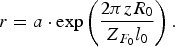 $$r = a \cdot \exp \left(\displaystyle{2\pi zR_0 \over Z_{F_0} l_0} \right).$$
B) Condition for the use of the derived design
Further considerations on the validity of equation (5) are necessary, since equation (3) is only valid for lines where transverse electromagnetic (TEM) waves propagate. By also using this equation for the region of the resistive layer it is assumed that a TEM wave propagates there as well. The propagation of the TEM wave in the region of the coaxial line and in the region of the coaxial resistance is illustrated by the blue lines in Fig. 2. The assumption of propagation of the TEM wave within the region of coaxial resistance violates two boundary conditions for the E-field. The first violated boundary condition is that the E-field has to be normal to the surface of a perfect electrical conductor (PEC) and thus to the surface of the outer conductor, which usually consists of excellent conducting material and can be assumed as the PEC.
The second violated condition is that the E-field propagating over a resistive film surface will be tilted away from the normal of the surface of the resistive film to the direction of propagation at a loss angle Ψ given by
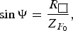 $$\sin {\Psi} = \displaystyle{R_{\squ} \over Z_{F_0}}\comma \;$$
where R □ is the sheet resistance given by
 $$R_{\squ} = 2\pi \cdot a \cdot \displaystyle{R_0 \over l_0}$$
and Z F 0 is the characteristic wave impedance. Because of the two generally violated boundary conditions for the E-field (in the same way, two conditions for the H-field are also violated, but it is sufficient to consider only the E-field), the question should be asked if and under what conditions it makes sense to taper the outer conductor exponentially according to equation (5) in order to minimize the reflection coefficient.
This question has been answered in [Reference Harris14] by making the assumption that the E-field phase fronts are spherical (green lines in Fig. 2) with radius ρ 0 and that their phase center lies on the z-axis. In this case, all the boundary conditions for the E-field in the resistance region are satisfied if the outer conductor is designed in the form of a tractrix. (Each tangent of the tractrix (outer conductor) cuts the asymptote (z-axis) at the same distance (ρ 0).) Furthermore, it has been proven that as long as the condition
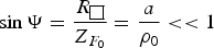 $$\sin \Psi = \displaystyle{R_{\squ} \over Z_{F_0}} = \displaystyle{a \over \rho_0}\lt \lt 1$$
is valid, the condition for TEM wave propagation in the resistive region is approximately satisfied and the TEM wave will propagate without any reflection.
In [Reference Kohn15], an exact equation for the tractrix profile of the outer conductor has been derived as
 $$\eqalign{&z = \displaystyle{l_0 Z_{F_0} \over 2\pi R} \left[\ln \displaystyle{1 - \sqrt{1 - \displaystyle{r^2 \over \rho_0^2}} \over \displaystyle{r \over \rho_0}} \right. \cr &\left. + \sqrt {1 - \displaystyle{r^2 \over \rho_0^2}} - \left(\ln \displaystyle{1 - \sqrt{1 - \displaystyle{a^2 \over \rho_0^2}} \over \displaystyle{a \over \rho_0}} + \sqrt{1 - \displaystyle{a^2 \over \rho _0^2}} \right)\right].}$$
By applying series expansions equation (9) becomes
 $$\eqalign{z & = \displaystyle{l_0 Z_{F_0} \over 2\pi R_0} \ln \displaystyle{r \over a} - \displaystyle{l_0 Z_{F_0} \sin^2 \psi \over 8\pi R_0} \cr &\times \left[\left(\displaystyle{r^2 \over a^2} - 1 \right) + \displaystyle{\sin^2 \psi \over 8} \left(\displaystyle{r^4 \over a^4} - 1 \right) + \displaystyle{\sin^4 \psi \over 24} \left(\displaystyle{r^6 \over a^6} - 1 \right) + \ldots \right].}$$
When the second part on the right-hand side of equation (10) is negligibly small, which is the case when the already known condition from equation (8) is valid, the obtained expression is exactly equal to equation (5).
To sum up, it can be said that the smaller the sheet resistance is, which means the longer the resistive layer is, the more equation (6) will be valid and the smaller |S 11| will be. However, since increasing the length of the resistive layer decreases the mechanical stability, a tradeoff between |S 11| and mechanical stability needs to be found.
C) Relative permeability compensation of ceramic substrate
It has been shown [Reference Harris14] that propagation of the wave inside a substrate with relative permittivity εr sub causes a reduction of the inductance ΔL of the line in this region according to
 $$\Delta L = - \pi \varepsilon_{r_{sub}} \left(\displaystyle{R_0 \over l_0}a \right)^2.$$
Up to now, the fact that the conductivity of the resistive layer is finite has been neglected. Owing to the finite conductivity the EM field will penetrate the resistive layer and propagate not only between the outer conductor and resistive layer but also inside the substrate. The case for a coaxial line with uniform outer conductor and one part of the inner conductor consisting of a substrate covered by a resistive layer shown in Fig. 3 has been investigated in [Reference Harris14].
Fig. 3. Uniform coaxial line with one part of the inner conductor consisting of a coaxial substrate covered by a resistive film. a and b are the radii of the inner and outer conductors of the coaxial line. a′ is the radius of the substrate and b′ is the radius of the outer conductor in the region of the resistive layer required in order to compensate for the reduction of the inductance caused by EM-field propagation inside the substrate.
It can be seen that the effect is independent of frequency and can therefore be compensated. A well-known approach to increase the inductance of a line is to increase the distance between the inner and the outer conductor. Thus, either the outer conductor should be designed with a bigger radius b′ or the inner conductor should be designed with a smaller radius a′ according to the formula
 $$\displaystyle{a \over a^{\prime}} = \displaystyle{b \over b^{\prime}} = 1+\displaystyle{\varepsilon_{r_{sub}} \sin^2 \psi \over 4}$$
derived in [Reference Woods16]. Although not exactly the same, the similar behavior can be expected for the case that the outer conductor has an exponential profile. The increased inductance for the 1 mm matched load considered in this paper was realized by decreasing the radius of the substrate. The start value of the substrate radius was calculated using equation (12) and fine tuned using EM simulations.
III. EM SIMULATIONS
A) Simulation model
The simulation model was set up according to Fig. 2 and is presented in Fig. 4. The length of the resistive layer was set to some millimeters, as a tradeoff between mechanical stability and |S 11|. By using the wave impedance of vacuum Z F 0 = 120π Ω, R 0 = 50 Ω and a = 0.217 mm, the outer conductor profile was designed according to equation (5) as
 $$r = 0.217\; {\rm mm} \cdot \exp \left(\displaystyle{5 \over 6l_0} \right).$$
In order to find the substrate radius that best compensates for the inductance ΔL, simulations with different radii were performed. The start value for the radius was calculated using equation (12). The excellent simulation results with the best substrate radius can be seen in Fig. 5. Here, the maximum |S 11| is only −43 dB over the entire frequency range from 0 to 110 GHz, which means that less than 0.7% of the EM wave was reflected.
Fig. 4. Model used for the 1-mm coaxial matched load in EM simulations. The diameters of the inner and outer conductors were set according to the IEEE standard [1]. The tapering of the outer conductor was designed according to equation (13). The start value for the substrate radius was chosen according to equation (12).
Fig. 5. |S 11| simulation and measurement results. The simulation results for a matched load with an exponentially tapered outer conductor performed with different simulation approaches are shown by: + HFSS, ∧ CST Frequency Solver, ○ CST Transient Solver. Simulation result for a predecessor model where the outer conductor was linearly tapered [17] is shown by x. * shows a typical measurement result for a produced matched load with exponentially tapered outer conductor.
B) Verification by different simulation approaches
The EM simulation was carried out with three different simulation approaches and two different simulation tools. In all three approaches, a waveguide port that represents an infinitely long waveguide connected to the structure was used for excitation. The inner and outer conductors were modeled as PEC.
In the first simulation approach, CST Microwave Studio [18] with transient solver and hexahedral mesh was used. Even though the real thickness of the resistive layer that covers the cylindrical ceramic substrate is in the range of some tenth of nanometers, it was modeled by a 5 µm thick layer. The resistivity was chosen such that the overall resistance was 50 Ω. The well-tried approach of using a 5-µm layer instead of the true value for simulations with CST Microwave Studio was used in this work. Before 2011, it was not possible to perform simulations of infinitely thin layers in CST, and the introduction of a resistive layer with a thickness of some hundreds of nanometers would have led to a dramatic increase in the number of mesh cells. By using a 5-µm thick layer and placing at least two mesh cells across the thickness of the resistive layer according to CST guidelines, the number of mesh cells could be kept below five millions.
A hexahedral mesh and a transient solver were used. At discrete locations and at discrete-time samples, the development of the fields over time is calculated by the Finite Integration Technique (FIT). Furthermore, an adaptive mesh refinement setting was used. With this setup, an initial simulation is run using an initial mesh. For subsequent simulations the mesh is refined. The higher the EM fields gradients in an area, the stronger the mesh refinement. The changes in S-parameters (ΔS) from one simulation to the next are compared to the adaptive convergence criteria being ΔS smaller as a certain set value for the entire frequency range from 0 to 110 GHz. At least two simulations have to be performed for the convergence criteria to be met. This setup prevents acceptance of the results of a simulation with an improper mesh.
The second approach used CST Microwave Studio with the frequency domain solver, a tetrahedral mesh and a resistive layer represented by an infinitely thin resistive layer (“Ohmic Sheet Resistance”). When using the CST frequency solver, FIT is still used for spatial discretization. In contrast to the hexahedral mesh, the tetrahedrons of the tetrahedral mesh conform to solid-boundaries, and the mesh refinement can be local with respect to all coordinate directions. The use of an Ohmic Sheet allows assigning a resistance to an infinitely thin layer of material. The EM fields in the simulation have the same magnitude on both sides of the Ohmic Sheet, but their direction in the vicinity of the Ohmic Sheet is determined by the loss angle, dependent on the specified value of the Ohmic Sheet. Thus, the Ohmic Sheet is a very good approximation of reality, where the resistive layer is only some tens of nm thick and determines only the loss angle and can be considered as “transparent” for the EM fields. Furthermore, since the Ohmic Sheet is infinitely thin, no mesh cells need to be placed inside the resistive layer. This means that the smallest mesh cell can be much larger than with a 5-µm thin layer and thus the amount of mesh cells can be kept low. The number of tetrahedrons was about 70 000 and the simulation time was much shorter than with a 5-µm thin layer. An adaptive mesh setting with the same convergence criterion as in the first approach was used.
The third approach was to use Ansoft HFSS [19]. HFSS uses the finite-element method in the frequency domain and tetrahedral meshes to divide the problem space into sub-regions for which Maxwell's Equations are then solved. The resistive layer in HFSS was modeled as infinitely thin. Using the “Lumped RLC Boundary” it is possible to define the resistance R, inductance L, and capacitance C in parallel to any surface. HFSS determines the impedance per square of the surface at any frequency. A resistive layer with properties R = 50 Ω, L = 0 H, and C = 0 F was assigned. The same stop criteria as in the first two simulation approaches were again used for the adaptive mesh refinement. The results found in [Reference Hoffmann, Leuchtmann and Vahldieck20] stating that the number of nodes on the circumference of the conductor and substrate need to be significantly increased in order to prevent the field simulator from producing modes strongly different from the coaxial TEM mode and thus from falsifying the result, could be confirmed.
The largest difference in the simulation results can be seen between the CST Transient Solver and the other two approaches. This is explained by different methods of modeling the resistive layer. This is also the reason why the number of mesh cells and the simulation time was significantly lower in the last two approaches as compared to the first approach. Furthermore, the simulations performed with HFSS were approximately six times faster than the simulations with CST in the second approach. A simulation result for a predecessor model as presented in [Reference Hechtfischer, Hohenester, Huber, Jünemann, Pinta and Völk17], where the outer conductor was linearly tapered, can also be seen. It is evident that tapering the outer conductor exponentially instead of linearly significantly improves the performance of the matched load.
IV. FABRICATION PROCESSES
The maximum reflection coefficient of −43 dB over the whole frequency range from 0 to 110 GHz achieved in EM-simulations is a satisfactory result. Therefore, the corresponding simulation model already shown in Fig. 4 became the starting point for the manufacturing model. The manufacturing model involves all the details required by the production process as specified in the engineering drawings. To avoid failures during the transfer of the simulation model to the manufacturing model and in order to investigate the impact of the manufacturing features on the reflection behavior of the matched load, the finished three-dimensional (3D) CAD model of the manufacturing model was imported into EM-simulation tools. The result of the EM simulation of the manufacturing model performed with HFSS can be seen in Fig. 6. The manufacturing features could be implemented with only a minimal increase in the maximum reflection coefficient. The production process for the coaxial 1-mm matched load with an exponential outer conductor was adapted from [Reference Hechtfischer, Hohenester, Huber, Jünemann, Pinta and Völk17]. A schematic view of a 1-mm male matched load with a tapered outer conductor can be seen in Fig. 7(a), the individual components in Fig. 7(b). First, the inner conductor consisting of a hard metal is produced by turning. Then, a gold layer is electroplated in order to increase the conductivity. The cylindrical ceramic substrate is produced by mechanical grinding. It consists of hipped Si3N4. This material was chosen based on its high bending strength, which makes the substrate resilient to mechanical stress. Furthermore, Si3N4 has a small relative dielectric constant that is almost frequency independent and can be compensated for as previously described.
Fig. 6. HFSS simulation results for the manufacturing model compared to the HFSS simulation results of the simulation model shown in Fig. 4. The manufacturing features could be implemented with only a minimal increase in the maximum reflection coefficient.
Fig. 7. (a) Geometry of the complete broadband matched load where the outer conductor has already been glued to a frame making the matched load manageable [17]. (b) Single components of the matched load (inner conductors, outer conductors, and coaxial substrates coated by resistive layer) compared in their size to a match.
The resistive layer on the substrate is realized by a NiCr alloy. The length of the resistive layer is equal to the length of the exponentially tapered region. The thickness of the alloy is chosen such that the total resistance value is slightly less than 50 Ω. Afterwards a laser trimming process is used to increase the resistance to exactly 50 Ω. The substrate is then soldered to the inner conductor. The production of the outer conductor starts by turning an aluminum part. The aluminum part has the negative form of the desired outer conductor. In the next step, gold is electroplated on the aluminum part to achieve high conductivity of the outer conductor. The thickness of the electroplated gold is chosen such that the outer conductor becomes mechanically stable yet remains slightly elastic. The aluminum part is then etched off and the outer conductor is finished.
The next production step consists of placing the inner conductor unit inside the outer conductor and soldering them together. The cylindrical form of the outer conductor in the region where it is soldered to the inner conductor leads to an exact centering between the outer conductor and inner conductor. To make the matched load manageable and to be able to screw it on the VNA ports, the outer conductor is glued to a frame as shown in Fig. 7(a)). The geometry of the matched load combined with the slight elasticity of the outer conductor allows it to withstand mechanical stress that can be introduced, for example, if the matched load is screwed to a coaxial line or to a VNA port where the inner conductor is not perfectly centered to the outer conductor, or if it is simply dropped.
V. RESULTS AND DISCUSSION
Finished matched loads were measured with an R&S ZVA 110 VNA [21] with a continuous sweep from 10 MHz to 110 GHz. A typical measurement result for a matched load with an exponentially tapered outer conductor is presented in Fig. 5. It can be seen that the shape of the curve coincides very well with the simulated curve shape.
In order to explain the difference in the magnitude of the simulated and measured |S 11| magnitude values, EM simulations were used to investigate the influence of manufacturing tolerances on |S 11|. The manufacturing tolerances (all in line with the specifications in the IEEE standard for coaxial 1-mm systems [1]) shown in Fig. 8 were swept simultaneously. The simulation results verified that the increase in |S 11| can be explained by manufacturing tolerances. This becomes obvious by considering the following simple example. If the diameter of the inner conductor is 5 µm too thin and the diameter of the outer conductor is 5 µm too thick, which is still within the tolerances of [1], the impedance of the line will change by 1.4 Ω and |S 11| will increase to −35 dB just because of these two deviations. The conclusion of the investigation is that in order to come even closer to the simulation results, manufacturing tolerances need to be even tighter than the specifications in the IEEE standard [1].
Fig. 8. Manufacturing tolerances whose influence on the matched load's reflection coefficient was investigated using EM simulations. (a) pd: pin depth; ds: diameter of the substrate; dic: diameter of the inner conductor; doc: diameter of the outer conductor; ffeoc: fluctuations in the position of the first edge of the outer conductor; fseoc: fluctuations in the position of the second edge of the outer conductor; sdoc: small diameter of the outer conductor; mfeocasrl: misalignment between the first edge of the outer conductor and the starting point of the resistive layer and (b) centricity of the inner conductor.
The introduction of a transmission region between the coaxial line and the region of the exponentially tapered outer conductor [Reference Kohn15] can be expected to further improve the reflection coefficient even beyond the simulated maximum of −43 dB. The transmission region should be used to bend the planar field of the coaxial line smoothly to the spherical field configuration presented in the region of the resistive layer. Replacing the abrupt change in the E-field lines found in the current design (see Fig. 2) with a smooth transition would lead to a further reduction in the maximum reflection coefficient and reduce it even beyond −43 dB.
VI. CONCLUSION
Matched loads with a maximum reflection coefficient | S 11 | of −32 dB over the frequency range from 0 to 110 GHz have been produced. Their ability to reach a maximum reflection coefficient |S 11| of −43 dB has been verified by EM-simulations. The EM-simulations have been performed in three different ways using two different simulation tools. The differences between the measured and simulated values were explained by manufacturing tolerances swept simultaneously during EM-simulations. The main features of the matched load design are an exponentially tapered outer conductor over a cylindrical ceramic substrate coated with a thin-film resistance, with compensation for EM wave propagation inside the resistive coating. Using such matched loads, it is now possible to calibrate VNAs very accurately with a single OSM, UOSM, or TOSM calibration technique over the entire frequency range, eliminating the time and effort involved in changing to another calibration technique at higher frequencies.
ACKNOWLEDGEMENTS
The authors would like to thank everyone who has contributed to the success of this work, especially W. Hohenester and C. Pinta.
Andreas Tag received his B.Sc. and M.Sc. degrees in Electrical Engineering from the Technische Universität München, Germany, in 2010 and 2012, respectively. He spent half of his Masters study period at the Chalmers University of Technology in Sweden. In September 2012, he joined the Institute for Electronics Engineering at the Friedrich-Alexander-Universität Erlangen-Nürnberg, Germany as a research assistant. He is currently working on his Doctor of Engineering degree (Ph.D.) in the field of the multi-physical modeling of micro acoustic RF MEMS components within the MUSIC (MUlti physical Synthesis and Integration of Complex RF circuits) research project funded by the German Research Foundation. Mr Tag's main research interests include RF MEMS, microwave measurement techniques and instruments, semiconductor devices and electronic design automation.
Jens Leinhos received the Dipl.-Ing. degree in Electrical Engineering from the Leibniz Universität Hannover, Hannover, Germany, in 2003. From 2004 to 2008, he was a Research Assistant at the Institute of Radiofrequency and Microwave Engineering at Leibnitz University Hannover and at Germany's national metrology institute (PTB) in Braunschweig, Germany. In 2008, he joined the R&D Department for Network Analysis at Rohde & Schwarz in Munich, Germany, where he develops RF network analyzer calibration kits. His current interest is the metrology for RF quantities including vector network analysis.
Gerd Hechtfischer received the diploma degree in physics from the Technische Universität München, Munich, Germany in 1994 and the Ph.D. degree in solid state physics from the University of Erlangen, Erlangen, Germany in 1997. His research activities have been focused on microwaves, superconductors, and thin-film technology. He is currently a team leader for microwave technology R&D at the Test and Measurement Division of Rohde Schwarz GmbH Co. KG in Munich, Germany. Dr. Hechtfischer received the Rohde Schwarz Innovation Award in 2009 and holds several patents.
Martin M. Leibfritz was born in Frankfurt, Germany, in 1977. He received the Dipl.-Ing. degree in Electrical Engineering and the Dr.-Ing. degree from the Universität Stuttgart, Stuttgart, Germany, in 2003 and 2007, respectively. From 2003 to 2007, he was a Research Assistant with the Institut für Hochfrequenztechnik, Universität Stuttgart. In 2007, he joined the Research and Development Department for Network Analysis, Rohde Schwarz, Munich, Germany. Since 2010, he is heading the development of vector network analyzers and profit center responsible at Rohde Schwarz, Munich, Germany. His main research interests are in antenna measurement techniques, antenna diagnostics, RF power amplifiers, and vector network analysis.
Thomas Eibert received the Dr.-Ing. degree in Electrical Engineering from Bergische Universität Wuppertal, Wuppertal, Germany in 1997. From 1997 to 1998, he was with the Radiation Laboratory, EECS Department at the University of Michigan, Ann Arbor, MI, USA, from 1998 to 2002, he was with Deutsche Telekom, Darmstadt, Germany, and from 2002 to 2005, he was with the Institute for High-Frequency Physics and Radar Techniques of FGAN e.V., Wachtberg, Germany, where he was the Head of the Department Antennas and Scattering. From 2005 to 2008, he was a Professor of radio frequency technology at Universität Stuttgart, Stuttgart, Germany. Since October 2008, he has been a Professor of High-frequency Engineering at the Technische Universität München, Munich, Germany. His major areas of interest are numerical electromagnetics, wave propagation, measurement techniques for antennas and scattering as well as all kinds of antenna and microwave circuit technologies for sensors and communications.

