


I. INTRODUCTION
Modern wireless communications systems require an increasing number of frequency bands, output power, efficiency, linearity, and development of circuits and subsystems to have broadband capabilities. These demands should be met within the existing radio base station (RBS) footprint where the cooling capacity and size are restricted with low network operating expenses (OPEX). The power amplifier (PA) is the most critical component in RBS since its performance strongly influence the overall system features in terms of bandwidth, output power, efficiency, and operating temperature. Therefore, various approaches are proposed to design ultra-wideband and efficient PAs. The common approach is based on optimizing the fundamental impedance, while resistive terminations are presented for higher order harmonics [Reference Colantonio, Giannini, Giofre and Piazzon1, Reference Andersson, Moon, Fager, Kim and Rorsman2]. Other approaches are based on continuous modes of operation, such as class-B/J, class-F, and inverse class-F [Reference Wright, Lees, Benedikt, Tasker and Cripps3–Reference Chen and Peroulis6]. However, most of the previously mentioned approaches have a low output power of <20 W. For high output power and ultra-wideband PAs, traveling wave amplifiers still the most preferable approach [Reference Ayasli, Reynolds, Mozzi and Hanes7], however with poor gain and efficiency across the desired bandwidth. To overcome these weaknesses, a harmonically tuned PA approach has demonstrated promising perspectives for the design of efficient, high-power, and ultra-wideband PAs [Reference Tanany, Gruner and Boeck8, Reference Arnous, Bathich, Preis, Gruner and Boeck9]. The conventional matching network (MN) using multi-stage Chebyshev low-pass filters is limited in bandwidth, due to the non-constant impedance transformation ratio of the MN over the desired band and the complexity of design a high-order filter. Therefore, impedance transformers are a sufficient solution for designing ultra-wide band MNs. Nevertheless, they are commonly used at low-frequency bands. Current developments present topologies implementing impedance transformers such as micro-coaxial system [Reference Ehsan, Vanhille, Rondineau and Popovic10], Marchand baluns [Reference Canning, Powell and Cripps11], or broadside-coupled PCB (printed circuit boards) [Reference Zhang and Boeck12] up to K-band frequencies with multi-octave bandwidths. The main goal of this work is to design and implement a high-power, multi-octave, and efficient PA. The wideband capability is achieved by utilizing broadside-coupled impedance transformers within the MNs. This paper is an extension and further work of [Reference Arnous, Zhang, Rautschke and Boeck13], where multi-octave, high-power amplifier using a planar transmission line transformer was introduced for the first time as a main part of the MN. In this paper, various transformer design approaches are introduced. A broadside-coupled planar taper transformer is used, due to its sufficient performance in terms of flat insertion loss (IL), return loss (RL), and bandwidth. The planar structure transformer results in simplifying the integration as well as the complexity of the MNs, which leads to improve the insertion loss.
The organization of this paper is as follows. The theoretical approach of transformer and implementation procedure are introduced in Section II, while the design approach and measurement results of PA using the transformer in input and output of the transistor are introduced in Section III. Finally, conclusion of this contribution is summarized in Section IV.
II. TRANSFORMER DESIGN APROACH
The general definition of transformers is to realize an impedance transformation between the input port and one or more outputs ports. The transformer can be classified into the following categories:
-
(1) Lumped element transformers,
-
(2) Coaxial and micro-coaxial transformers [Reference Ehsan, Vanhille, Rondineau and Popovic10],
-
(3) Planar transformers [Reference Zhang and Boeck12].
The first, lumped element transformer is limited in terms of frequency because of losses and the physical dimensions limiting the cut-off frequency for lumped components. In case of the coaxial transformer, the manufacturing effort increases with higher frequencies and mounting becomes more and more complex. The planar transformer approach based on Guanella transformer approach [Reference Guanella14] is the most promising solution in terms of complexity, cost, bandwidth, and IL.
A) Theoretical approach of the transformer
The used transformer in this work consists of two transmission lines with a characteristic impedance Z C connected in parallel at the transformer input plane and in series at transformer output plane. Consequently, the impedance seen at the input plane is the half of the characteristic impedance (Z C /2), and the impedance seen at the output plane is double of the characteristic impedance (2·Z C ), as shown in Fig. 1(a). In this case, the resulting transformation ratio is 4:1. The two-layer schematic, including coupled microstrip lines (MSL) and via connection, for this design is depicted in Fig. 1(b).

Fig. 1. (a) Design concept of broadside-coupled planar transformer. (b) Schematic of transformer.
The characteristic impedance Z C needs to be 25 Ω to realize a broadband transformation from 12.5 to 50 Ω. For high bandwidth, the characteristic impedance ratio of even and odd mode of the broadside-coupled suspended MSL must be high to ensure a tight coupling. Thus, the distance between bottom MSL and ground shield is an important factor. As larger the distance to the ground shield, as larger is Z even and an efficient broadband transformation is possible. A shielded stripline assumption is intended to illustrate this concept. Figures 2(a) and 2(b) depict the electrical field lines for even and odd modes for two broadside-coupled shielded striplines (ε 1 = ε 2 = 1) [Reference Mongia, Bahl, Bhartia and Hong15]. The following equations (1) and (2) represent the even- and odd-mode characteristic impedance of broadside-coupled suspended MSL (ε 1 = 1 < ε 2), which are derived from the shielded stripline model [Reference Mongia, Bahl, Bhartia and Hong15].
 $$Z_{0,e} = \displaystyle{{Z_{0,e}^a} \over {\sqrt {\varepsilon _{r,e}}}}, $$
 $$Z_{0,o} = \displaystyle{{Z_{0,o}^a} \over {\sqrt {\varepsilon _{r,o}}}}, $$
where
 $Z_{0,e}^a $
is even mode impedances of the air-filled stripline model;
$Z_{0,e}^a $
is even mode impedances of the air-filled stripline model;
 $Z_{0,o}^a $
odd-mode impedances of the air-filled stripline model; ε
r, e
the effective relative permittivity for even mode; ε
r, o
the effective relative permittivity for odd mode.
$Z_{0,o}^a $
odd-mode impedances of the air-filled stripline model; ε
r, e
the effective relative permittivity for even mode; ε
r, o
the effective relative permittivity for odd mode.

Fig. 2. (a) Electrical field lines even mode, (b) Electrical field lines odd mode for shielded broadside-coupled lines. (c) Even and odd-mode impedances versus shield distance.
The most important factor for a broadband transformation is the coupling (C) between the two lines, as presented in equation (3). It can be simplified by the assumption that β l = π/2. This leads that the coupling only depends on the impedance ratio c, as shown in equation (4), which should be close to unity [Reference Zhang and Boeck12]. Therefore, the large even-mode impedance has to be realized using a sufficient large distance for the ground shield of broadside-coupled suspended MSL.
 $$C = 20 \cdot {\rm log}\displaystyle{{(1 - c^2 \cdot {\rm cos}^2 \beta l)^{1/2}} \over {c \cdot {\rm sin}\beta l}},$$
 $$c = \displaystyle{{Z_{0,e} - Z_{0,o}} \over {Z_{0,e} + Z_{0,o}}}. $$
Figure 2(c) depicts the simulation results for the even- and odd-mode impedances of two coupled suspended MSL with a width of 3.1 mm in dependence to the distance of the ground shield. The figure illustrates that increasing the distance results in increasing the even characteristic impedance; nevertheless, cavity cannot be infinity. Therefore, 10 mm is a reasonable distance to be used. The resulting impedances of even- and odd-mode impedances are 400 and 12.5 Ω, respectively.
B) Practical approach of the transformer
Two transformer topologies are simulated, implemented, and measured. The first one (Top I) is based on [Reference Zhang and Boeck12], as shown in Fig. 3; whereas the second one (Top II) is modified and uses a tapered ground plane (Fig. 3(d)), for a smooth transition instead of a MSL as in Top I (Fig. 3(c)), to ensure a high transmission coefficient, less radiation losses, and lower parasitic impact. The top metallization is the same for both structures. The figure also presents the manufactured prototypes of the transformer. Both topologies were fabricated using Rogers RO4003c substrate with a total size of 34 × 37.5 mm2 for Top I and 24 × 37.5 mm2 for Top II, and a thickness of 508 µm. The area of Top II is decreased by almost 30% compared with Top I.

Fig. 3. (a) Three-dimensional view of realized transformer. (b) Top side photograph of transformer. (c) Bottom side photograph of Top I. (d) Bottom side photograph of Top II.
The measurement was done on 50 Ω SMA (subminiature A connector) reference plane using a Rohde & Schwarz ZVC vector network analyzer, which is capable of handling frequencies up to 4 GHz. The usage of a test fixture can guarantee a sufficient large distance to the ground shield. Both SMA connectors, input, and output, were de-embedded with a self-developed model in Keysight ADS (Advanced Design System). The de-embedded measurement results of the two topologies are presented in Fig. 4.
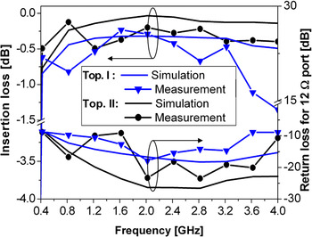
Fig. 4. Simulation and measurement results of the manufactured transformers.
There is a good agreement between measurement and simulation for both topologies. Top II observes a more flat and better IL compared with Top I with a value of <0.5 dB and a RL of 15 dB over a decade bandwidth 0.4–4.0 GHz. Therefore, Top II is used to as a main part of the MN to design the desired PA.
III. DESIGN METHODOLOGY OF THE ULTRA-WIDEBAND PA
Designing high-power and efficient PAs for multi-octave bandwidth is quite challenging. Large periphery devices are required to obtain high power. Therefore, the bandwidth is restricted because of the high device capacitances (C DS , CGS ), and low optima source/load impedances. In this respect, the high breakdown voltage and high output power density of gallium nitride-high electron mobility transistor (GaN-HEMT) devices have significant advantages in terms of power and bandwidth.
A) Device characterization
A CGH40120F device by Wolfspeed Inc. with a saturated output power of 120 W is used [16]. This device is based on a 400 nm gate length GaN technology which can handle a high breakdown voltage up to 85 V. The optimum operating point for maximum transconductance is stated at V DD = 28 V and I DQ = 1 A. At this operating point the simulated extrinsic transit frequency is about f T = 8.5 GHz with a maximum oscillation frequency of f MAX = 18 GHz, which makes the device suitable for mobile communication systems. Figure 5(a) illustrates the maximum available gain (MAG) and MSG (maximum stable gain) of the device versus frequency at various drain voltages and quiescent currents. Increasing the drain voltage results in a larger MAG and output power. However, the usable frequency band decreases and the dissipated power (P diss ) of the device increase, as shown in Fig. 5(b). Therefore, a compromise between these factors is considered with a drain biasing of V DD = 32 V and I DQ = 0.5 A, where a high MAG with a low DC-power consumption is available up to 2.7 GHz.

Fig. 5. (a) MAG of CGH40120F at various bias conditions. (b) P diss versus various biasing.
B) MNs approach
In this context, source/load pull simulations, using the accurate large-signal transistor model from Wolfspeed Inc., have been performed. The effect of the harmonics in source/load impedances on output power and efficiency were analyzed and considered in the design to enhance the efficiency over the desired band. Based on [Reference Arnous, Bathich, Preis, Gruner and Boeck9], only up to second harmonic impedances should be considered during the load pull analysis, whereas the influence of the all harmonic source impendences and third load harmonic were omitted, due to their minor effect compared with the complexity introduced to the design of the MNs. However, the in-band harmonics is the bottleneck of this work, as shown in Fig. 6. This problem can be solved using the advantage of the high MAG of the device at low-frequency range to modify intentionally the optima fundamental load impedances of the low-frequency band (F L0) and middle-frequency band (F M0) from their optimum value, but in the same safe optimum range, ensure a 100 W output power. In other words, a mismatch is purposely chosen for the fundamental impedance at F L0 and F M0 band. Consequently, lower gain is available and the impact of higher harmonics (H·F 0) is minimized. Figure 7(a) shows an example of modifying the optimum load impedance of 0.6 GHz.

Fig. 6. Desired bandwidth frequency ranges fundamental and harmonics.

Fig. 7. (a) Load impedance locus at 0.6 GHz. (b) Optima fundamental impedances Z L, opt of the transistor, pre-MN topology to match Z L, opt to 12.5 Ω and broadside-coupled transformer to match it to 50 Ω.
The optima source/load impedances of large periphery devices are low and require broadband impedance transformations from 50 Ω to a low complex load. In this respect, the designed MN topology should consist of two parts which can be observed independently. The first one transforms the 50 Ω impedance plane to 12.5 Ω. This transformation will be achieved using a broadside-coupled 4:1 transformer based on the presented concept in Section II. Whereas, the second one matches the broadside-coupled transformer low-impedance plane to the extracted optima complex impedances of the device Z opt , as shown in Fig. 7(b). The extracted optima fundamental source/load impedances for the low frequencies were slightly modified reducing the influence of the harmonics. Consequently, the high-gain response at these frequencies, as shown in Fig. 5(a), is decreased and results in more flat gain within bandwidth of operation.
Based on this study, the desired bandwidth of the PA is defined over 0.6–2.6 GHz. The transformer is used at both sides of the device. The measured results of transformer is imported, de-embedded and used as a reference plane for the pre-MN s. The main aim of the pre-MN is to match the complex extracted optima source/load impedances of the transistor to the transformer de-embedded low-impedance plane across the desired bandwidth. Therefore, lossless two stage L-type Chebyshev low-pass filter is used considering the in-band problem. Furthermore, the modified optima load impedances overcame the pre-MN challenges in term of bandwidth. The per-MN structure is symmetrically designed to ensure a homogeneous wave distribution through the network. Moreover, a stability factor higher than unity is precisely considered to avoid oscillation of the PA by choosing an appropriate stability circuit, as shown in Fig. 8.

Fig. 8. Block diagram of the ultra-wideband PA.
The MNs are implemented with a size of 60 × 160 mm2 and a heat sink height of 20 mm (10 mm is the height of cavity bellow the input/output transformers). The total circuit without the active device was evaluated using a 50 Ω MSL instead of the transistor. The forward transmission (S 21) measurement results show a good agreement with the simulation (schematic and ADS 2.5D-Momentum) across the desired bandwidth with a minimum value of −4.5 dB, as shown in Fig. 9. These losses are basically related to the R GS resistor which is used to stabilize the designed PA, and the mismatch, due to the replacement of the transistor with a 50 Ω MSL.

Fig. 9. Through and RL comparison of the whole design using 50 Ω MSL instead of the active device between simulated schematic (solid line), ADS 2.5D-Momentum (discrete line) and measured (symbols) results.
C) Experimental results
The whole PA is implemented on Rogers RO4003c substrate with ε r of 3.55 and thickness of 0.508 mm. Figure 10 shows the prototype of the design. The implemented broadband PA has been characterized by its small- and large-signal measurements to evaluate its performance. Measurements were performed at a drain bias voltage of 32 V and quiescent current of 0.5 A. Preliminary experimental results show a good agreement with the simulated data over the design band.

Fig. 10. Prototype of the fabricated PA.
1) SMALL-SIGNAL MEASUREMENTS
Small-signal measurements were done using a Rohde & Schwarz ZVC vector network analyzer, which is calibrated using a TOSM calibration kit at the SMA reference plane. The comparison between simulated and measured small-signal gain and input reflection of the fabricated PA is presented in Fig. 11. The measured RL is in agreement with simulated results across the bandwidth, whereas the measured gain of the designed PA is subsequent to the simulated gain with a minimum value of 12 dB over the 0.6–2.6 GHz.

Fig. 11. Comparison between simulated and measured small-signal gain & reflection coefficient performance at V DD = 32 V & I DQ = 0.5 A.
2) LARGE-SIGNAL MEASUREMENTS
Large-signal measurements were performed using a continuous wave (CW) input signal generated by a microwave signal generator (Agilent E4438C) boosted by a microwave driver amplifier from Mini-Circuits Inc. The relevant output power was measured by a calibrated power meter (Agilent N1912A). A non-flat pre-amplification is compensated by a Matlab controlled measurement system. Both input and output power of the DUT (device under test) were measured simultaneously. This setup was calibrated to the SMA reference plane.
Figure 12 reports the comparison between simulated and measured output power, power gain, and drain efficiency as functions of the frequency. As can be observed, the measured results have a good agreement with the simulated ones. A maximum output power of 49.6 ± 1 dBm, minimum drain efficiency of 50% and large-signal gain of 10 ± 1.5 dB across 0.6–2.6 GHz is achieved. Figures 13(a) and 13(b) illustrate the measured saturated output power and power added efficiency (PAE) with respect to the CW input power at various frequencies. The measured PAE is between 42 and 60%.

Fig. 12. Comparison between simulated (solid lines) and measured (symbols) maximum output power, power gain, drain efficiency across the bandwidth at V DD = 32 V, I DQ = 0.5 A.

Fig. 13. (a) Output power and (b) power added efficiency for various frequencies versus input power at V DD = 32 V, I DQ = 0.5 A.
Besides CW measurements, harmonic distortion is an interesting factor in broadband PA design, especially for mobile communication. Figure 14 shows the measured second and third-harmonic distortion power level relative to the fundamental frequency output power at various output power levels and different frequencies. The chosen frequencies are 0.7 GHz, its second and third harmonics are located within the band of operation, 1.4 GHz, its second harmonic is at the edge of the band and third harmonic is out of band, and finally 2.0 GHz, where the harmonics are out of band.

Fig. 14. Measured second and third relative harmonics level versus output power at 0.7, 1.4, and 2.0 GHz fundamental frequencies at V DD = 32 V, I DQ = 0.5 A.
This measurement proves, that the harmonics output power in band has higher harmonics level ranges from −21 to −12 dBc compared with the harmonics output power out of band, which ranges from −56 to −35 dBc.
IV. CONCLUSION
The design of a high-power, multi-octave, and high-efficiency PA was presented in this paper. The bandwidth restriction was solved using an efficient ultra-wideband transmission line transformer. A ground tapered MSL was used to achieve flat and low IL and high RL. The transformer was integrated with the input and output MNs. The measured results show a good agreement with simulation with a maximum output power of 50.6 dBm, an average drain efficiency higher than 50% and flat gain of 10 ± 1.5 dB. The harmonics distortion power level relative to the fundamental frequency was evaluated at in-band and out-of-band operation. The in-band harmonics have a higher harmonics distortion compared with the out-of-band frequencies. Finally, a performance comparison of the presented PA with state-of-the-art results for efficient, high-power wideband PAs is summarized in Table 1. The comparison shows the excellent performance of the designed PA and thereby demonstrates the usefulness of the proposed approach for the design of efficient, high-power, and wideband PAs for future wireless systems.
Table 1. State-of-the-art 100 W wideband GaN-PAs.

* Two devices in parallel.
† Four devices push–pull.
ACKNOWLEDGEMENTS
The authors would like to acknowledge Wolfspeed Inc. for providing the large-signal model of the device, Modelithics Inc. for providing the whole library of their ATC capacitors and GloMic GmbH for continuous interest and advice. This work was supported in part by Deutsche Forschungsgemeinschaft (DFG) under grant number BO1520/9.
 Mhd. Tareq Arnous was born in 1984 in Damascus, Syria. Received the B.Sc. degree in Telecommunication and Electrical Engineering from Damascus University, Syria, in 2009, the M.Sc. degree in High Frequency Technique from the Berlin Institute of Technology, Germany in 2012. Since then, he has been working toward the Ph.D. degree with Microwave Engineering Laboratory at Berlin Institute of Technology. His main research interests include efficiency and bandwidth enhancement techniques GaN-based power amplifiers using dynamic load modulation. Currently, he is working at TDK as RF-module developer. Mr. Arnous was the recipient of the IEEE MTT-S Young Scientist Contest prize of the 20th International Conference on Microwave, Radar and Wireless Communications in 2014. He received as well the Student Design Competition Award for a Microwave Power Amplifier Design at the German Microwave Conference in 2015. Recently, he received the Young Scientist Contest distinction award at the 21th International Conference on Microwave, Radar and Wireless Communications 2016.
 Zihui Zhang received the Dipl.-Ing. Degree in Electrical Engineering from the Berlin Institute of Technology, Germany in 2009. Currently, he is working toward his Ph.D. degree with the Microwave Engineering Laboratory at Berlin Institute of Technology. His main research areas are high-efficiency power amplifier design for arbitrary load impedances as well as power combining based power amplifiers. He is the founder and CEO of Smart Devices GmbH.
 Felix Rautschke (S15) was born in Chemnitz, Germany. He received the B.Sc. degree, 2012, and the M.Sc. degree, 2014, in Electrical Engineering at the Chemnitz University of Technology. He is currently working toward the Ph.D. degree in the Microwave Engineering Research Laboratory at Berlin Institute of Technology. His research interest is in the area of broadband GaN microwave amplifier design. Recently, he received the Young Scientist Contest GAAS Association Prize at the 21th International Conference on Microwave, Radar and Wireless Communications (MIKON).
 Georg Boeck (M'93-SM'00-F'08) received his Ph.D. degree from the Berlin University of Technology, Berlin, Germany with honors, in 1984. In the same year, he joined Siemens Research Laboratories, Munich, Germany, where his research areas concerned fiber optics and GaAs electronics. Since 1991, he has been head of the Chair in Microwave Engineering with the Berlin Institute of Technology, Berlin, Germany. His areas of research involve the design and modeling of devices and circuits up to the THz range with a focus on the development of high-efficiency power amplifiers and smart transceiver systems for modern digital communications technologies. He has authored or co-authored more than 340 technical papers and one book. He chaired several international conferences, served in numerous steering and technical program committees and editorial boards of international journals. From 2006 to 2008, he was recognized from the IEEE MTT society as “Distinguished Microwave Lecturer” and was appointed as a guest professor at Southeast University Nanjing, Nanjing, China.


