


INTRODUCTION
Large three-dimensional maps of microstructures based on orientation imaging microscopy (Adams et al., Reference Adams, Kunze and Wright1993; Wright and Adams, Reference Wright and Adams1992) have become accessible in the past few years due to the availability of automated serial sectioning and dual beam microscopes with focused ion and electron beams (Uchic et al., Reference Uchic, Groeber, Dimiduk and Simmons2006; Lee et al., Reference Lee, Rollett and Rohrer2007). The drawback to these measurements is that they, of necessity, destroy the measured material as sectioning proceeds. High energy X-ray diffraction microscopy (HEDM) (Poulsen, Reference Poulsen2004; Suter et al., Reference Suter, Hefferan, Li, Hennessy, Xiao, Lienert and Tieman2008; Lienert et al., Reference Lienert, Almer, Jakobsen, Pantleon, Poulsen, Hennessy, Xiao and Suter2007; Suter et al., Reference Suter, Hennessy, Xiao and Lienert2006) is one of the several new X-ray techniques (Ludwig et al., Reference Ludwig, Schmidt, Lauridsen and Poulsen2008; Larson et al., Reference Larson, Yang, Ice, Budai and Tischler2002) that permit spatially resolved nondestructive measurement of volumes of polycrystal microstructures. These techniques allow the monitoring of responses of ensembles of grains as various thermomechanical stimuli are applied and thus open the way to directly constraining theoretical models of microstructure response. HEDM, a synchrotron based technique, is able to map three-dimensional macroscopic volumes of microstructures at micron-scale resolution with better than 0.1° orientation resolution.
This paper characterizes minimum uncertainties and noise levels in reconstructed microstructure maps. Simulated diffraction data sets are generated from artificial (and thus known) microstructures. The analysis software then uses these data sets to attempt to reconstruct the initial microstructure. By comparing initial and reconstructed structures, we obtain several quantitative measures of the precision and accuracy of crystallographic orientation and real space geometry determinations. Two synthetic microstructures, one with a small number of large grains and the other with a large number of small grains, are treated, each with two different simulated detectors having different spatial resolutions.
The HEDM microstructure mapping measurement has been described in detail elsewhere (Lienert et al., Reference Lienert, Almer, Jakobsen, Pantleon, Poulsen, Hennessy, Xiao and Suter2007; Suter et al., Reference Suter, Hennessy, Xiao and Lienert2006; Poulsen et al., Reference Poulsen, Nielsen, Laurdisen, Schmidt, Suter, Lienert, Margulies, Lorentzen and Juul Jensen2001); here, we give a brief summary. The experimental geometry is shown in Figure 1. A line focused (∼2 μm high by 1.3 mm wide), high energy (>50 keV), monochromatic X-ray beam illuminates a planar cross section of the sample. Samples are typically wires up to 1 mm in diameter so that the entire cross section remains in the beam as the sample rotates about the ω axis. Diffraction from individual grain cross sections is imaged with a near-field (L=4 to 10 mm) charge-coupled device (CCD) based area detector that is positioned normal to the incident beam and downstream of the sample (Lienert et al., Reference Lienert, Almer, Jakobsen, Pantleon, Poulsen, Hennessy, Xiao and Suter2007). Diffraction images are collected as the sample is
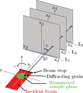
Figure 1. (Color online) Schematic of HEDM grain mapping measurement technique. A line focused X-ray beam illuminates a planar section of the sample. The sample is rotated about the z axis perpendicular to the illuminated plane (angle ω). A high resolution CCD based detector measures diffraction patterns at two or three rotation axis-to-detector distances, xd=L1,L2,L3. Scattering angles 2θ and η and the position of origin inside sample are encoded in the observed Bragg spot positions.
rotated about the ω axis over a small integration interval, δ ω (typically 1°). The shape of an observed Bragg spot (ellipses on the detectors in Figure 1) is, to first order, the projection along the outgoing wave vector of the diffracting grain’s cross-sectional shape. Such images are collected over a range in ω of up to 180° so that each grain produces many (50 to 60 for cubic structures) Bragg peaks and thus yields many projections along different directions relative to the grain. Detector images may contain several to hundreds of Bragg peaks (depending on the coarseness of the microstructure) originating from different locations in the polycrystal. The detector resolution determines the precision with which Bragg spots can be measured and, thus, the precision of the reconstructed microstructure geometry.
The generation of orientation maps of measured polycrystal cross sections is achieved with a forward modeling reconstruction procedure. The term “forward modeling” is meant to imply that, rather than attempting to invert the image data through back projections from the detector into the illuminated plane, we simulate the sample and data collection procedure and forward project simulated scattering onto the detector. The goal is to adjust the simulated sample orientation field to achieve an optimized match of simulated scattering to the experimental detector image data. The modeling procedure takes as inputs a set of geometrical parameters describing the apparatus (L distances, detector origin positions defined as the intersection of the projection of the beam and the rotation axis onto the detectors, detector orientation errors, and X-ray beam energy), the sample crystal structure, and the detector images. At present, we use a simplified binary representation of the images: experimental images are background subtracted and peaks are thresholded so that pixels are either “hit” or not. Future work will incorporate intensity matching. A preliminary step to doing a reconstruction is to determine precise values of the apparatus parameters through a boot-strapping procedure that optimizes the quality of reconstruction of a calibration sample or a set of judiciously chosen positions in a measured sample (this will be described in a forthcoming publication).
In the model, the illuminated sample plane is tiled with a mesh of equilateral triangles. The triangle size sets the geometric resolution of the reconstruction; ideally, this should be the size of detector pixels or smaller. Meshes can become quite large: 3 μm triangles spanning millimeter samples imply 105 elements per layer. In each triangle, the computer code searches the crystallographic orientation space to maximize overlap between simulated Bragg scattering and experimentally observed scattering peaks. Correct orientations will generate Bragg peaks that pass through experimentally observed diffraction spots at multiple L’s. Since each element produces 50 to 60 peaks that project to different locations on the detector, at different L distances, and within different δ ω intervals, the orientation is determined by comparing to the entire data set—this leads to tight constraints on orientations with a resolution of ∼0.1°, as shown below. As this description implies, the orientation in each triangular element can be determined independently from all others. This makes the computation easy to parallelize and we take advantage of the availability of highly parallel architectures.
Hardware at the 1-ID B hutch, data collection procedures, and analysis code have all evolved significantly over

Figure 2. (Color online) Simulated two-dimensional microstructures. (a) contains 32 distinct orientations or grains, while (b) has 497 grains. Shades (colors) are mapped using an axis-angle representation of the crystallographic orientation. Hence, regions of similar shades (colors) correspond to similar orientation.
the past year and we anticipate continued upgrades. For example, new CCD cameras with higher pixel resolution, more pixels, and faster readout have been commissioned. With improved readout times, we have begun to collect larger data sets both in terms of the number of cross sections (i.e., larger volumes) and the number of rotation intervals sampled. Given this fluid situation, we have developed a series of simulation tests to analyze the efficacy of new hardware and experimental protocols. The goal is to assure robust orientation and geometrical reconstructions in advance of data collection so that we optimize the use of synchrotron beam time.
Below we present simulations in which detector images are directly generated by the forward modeling software using simulated microstructures and realistic experimental geometry and detector parameters. In the reconstructions, we use the known experimental parameters and ask what errors remain if these are perfectly known: What is the effect of discretization of the scattering due to finite sized square detector pixels? What is the effect of using finite δ ω integration intervals? What is the mitigating effect of measuring many Bragg peaks over a large ω range?
II. GENERATION OF MICROSTRUCTURES AND FITTING PROCEDURES
The artificial microstructures used for the verification tests are shown in Figure 2. The microstructures are generated by producing simulation boxes that would enclose a centered 1 mm diameter sample, indicative of the cylindrical wires used in the HEDM experiments. Each simulation box is composed of six triangles with 0.6 mm sides and which are referred to as generation zero or g=0 triangles. The grid is made finer by subdividing each triangle into four equilateral triangles with half the side length of the parent. G is incremented with each successive regrid. Thus, triangle side lengths are (0.6 mm)/2g, and there exist 6×4g elements after all triangles have been regrid g times.
The maps in Figure 2 contain 32 and 497 grains. The average size in (a) is 190 μm (circle equivalent diameter) with variation in area from 5159 to 67 217 μm2. While most grains would be characterized as “equiaxed,” there are some with quite anisotropic shapes. In (b), the average diameter is 50 μm with areas spanning 140 to 6489 μm2. The range of grain sizes and shapes in the two simulated structures is comparable to the range that we have measured in real samples. The partitioning of the simulated structure into the grains was achieved by a Voronoi tessellation procedure, which resulted in no two grains having the same size. Each grain is assigned a single orientation chosen from a list of uniformly distributed orientations, such that the misorientation between all grains exceeds 5°. The simulated microstructure for the 32-grain set is composed of g=5 triangles with 19 μm sides, while the 497-grain set is composed of g=6 triangles, with 9 μm sides.
Using the forward modeling software, each microstructure produced its own set of simulated detector images. To mimic the binary reduced experimental data, detector pixels were set to 1 if the Bragg diffraction from any triangle hits them and zero otherwise. Two data sets were generated for each structure. The first used a simulated detector with 1024×1024 pixels with a pitch of 4.0 μm/pixel and rotation axis-to-detector distances, L i, of 4.75, 6.75, and 8.75 mm. Simulated diffraction images consist of 100 1° integration intervals. A planar monochromatic X-ray beam of 50 keV illuminates the entire simulation box. Pure fcc aluminum (lattice constant a=4.05 Å) is used as the simulated sample material. In generating the scattering, only Bragg peaks that are visible at all three detector distances were produced. Therefore, only scattering up to the wave vector transfer Q=12 Å−1 is maintained in the analysis, leaving {137} Miller index reflections as the largest diffraction ring. The second simulation set used a 2048×2048 camera with 1.5 μm/pixel, a photon energy of 65.35 keV, L i=7,11,15 mm, and aluminum scattering. The omega sampling for this setup included 180 integration intervals of 1°. The latter parameters mimic our most recent data collection run.
The forward modeling code searches orientation space for crystallographic orientations that generate scattering that matches experimental scattering found in the input data set. This search is done independently for each individual triangle. While Monte Carlo optimization of orientations uses a cost function based on maximizing pixel overlap between the reconstructed and input data sets, the acceptance of candidate orientations is based on a confidence parameter, C, equal to the fraction of reconstructed peaks that overlap experimental scattering at multiple L positions (Suter et al., Reference Suter, Hennessy, Xiao and Lienert2006, Reference Suter, Hefferan, Li, Hennessy, Xiao, Lienert and Tieman2008). The fits are accelerated by retaining and updating, as the fit proceeds, a list of orientations that have been found so far. New orientations are added to this list if they satisfy a strong convergence criterion, C s, and there are no other list entries within some misorientation threshold (usually 2°). C s is a value of the confidence parameter that gives strong assurance that the reconstructed orientation assignment is correct (C s=0.85 in the current fits). In the search for an orientation for a given triangle, the algorithm (i) starts with the triangle’s previous orientation if present (this occurs if we have regridded a previously fitted triangle to achieve finer resolution; the smaller regridded triangles are initially given the orientation of the parent triangle), (ii) tests the list of previously found orientations described above, and finally (iii) exhaustively searches over all of the orientation spaces. If the strong convergence condition is reached at any point, the search is stopped and the result is accepted. If no strongly converged
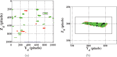
Figure 3. (Color online) Sample diffraction image using the 1k×1k detector for the 32-grain data set corresponding to the microstructure in Figure 2a. The boxed diffraction spot in (a) is shown in (b), displaying all three pixel types. The majority of spots (light shades in (a), green in on-line version) indicate fitted intensity that hits pixels in the simulated data set. A very small percentage of pixels in the simulated data set. A very small percentage of pixels (black in on-line version) contain simulated diffraction not hit by the fit and are visible in the interior of the spot in (b). Pixels that are hit by the fit, but are not in the simulated data set are intermediately shade (red in color version). Six spots composed of these ‘fit only’ pixels are seen in (a), as well as dotting the perimeter of the diffraction spot in (b).
orientation is found, then the orientation with the greatest confidence larger than a weak criterion, C w, is accepted. If C w is never attained, then the triangle is marked as unconverged and is assigned no orientation. Discussion of these and alternate optimization procedures will be described in a forthcoming publication.
The fits to the 1k×1k detector data sets used a regridding procedure as follows: (i) the triangular reconstruction mesh was uniformly gridded to g=g s i m−1, where g s i m=5 was the size of the triangles used to generate the simulated data set; (ii) triangles of this reconstruction mesh were fitted to the simulated data; (iii) reconstruction triangles that did not converge (C<C w), only weakly converged (C w≤C<C s), or were found to have neighbors with distinct orientations were regridded to g=g s i m; (iv) all regridded triangles were refitted; and (v) a boundary checking procedure was applied in which any triangle with a neighbor of distinct orientation was tested with that neighbor’s orientation and the strongest convergence value was kept. The fits to the 2k×2k detector simply regridded to the exact mesh used to generate the simulated data sets (g s i m=6), fitted the mesh, and performed the boundary checking procedure. As stated above, experimental parameters for the reconstructions were fixed to the values used to generate the data set.
III. RESULTS AND DISCUSSION
Figure 3 is a diffraction image on the 1k×1k detector generated from the 32-grain microstructure and corresponding to a single 1° integration interval at distance L 2=6.75 mm. The images from the 497-grain set are similar but with a larger number of smaller spots. Figure 3 represents one of the 300 images that form the data set. The union of green and black pixels (visible in online version of article) is the input simulated diffraction, while the union of green and red pixels originates from scattering produced by the reconstructed microstructure (see discussion below). With the perfectly ordered simulated grains in the input microstructure, each input diffraction spot is a pixilated projection

Figure 4. (Color online) Misorientation angles between reconstructed microstructures and their corresponding triangles in the input simulated microstructure: (a) 32-grain and (b) 497-grain cases. These maps are from reconstructions using a 1k×1k detector. Black lines indicate grain boundaries in the input structure. Triangles with misorientations larger than 0.3° are shown in white; there are none in (a) and 914 in (b). To illustrate these white triangles, (c) magnifies the bottom right corner of the map in (b).
of one of the grains onto the detector (along the scattering vector) when the sample is at this particular ω. The horizontal extent of the spots is approximately the y-direction extent of the grain (see Figure 1). To first order, the vertical extent of diffraction spots is due to the extent of the grain along the incident beam propagation direction, x, but this projection is a strong function of the orientation of the scattering vector: scattering at small |η| (see Figure 1) yields relatively extended spots whereas |η|∼90° yields a thin line as seen at the lower left of Figure 2a. (Poulsen, Reference Poulsen2004; Suter et al., Reference Suter, Hennessy, Xiao and Lienert2006)
We compare the reconstructed microstructures to the initial simulated microstructures in several ways. Figure 3 indicates the extent of overlap between the simulated data set and the reconstructed diffraction peak patterns: the vast majority of pixels illuminated by the reconstruction are in the input data set (green). There are some red diffraction spots indicating that the reconstruction hits regions with no simulated input scattering present. In each case, however, these are diffraction spots that appear on images in neighboring ω intervals; this indicates that some orientation noise is present and, for peaks that occur at the edges of ω integration intervals, some triangles converge to orientations that generate scattering in incorrect intervals. This noise could be reduced or eliminated by a more strict convergence criterion, C w. However, we choose to use the procedure described in Sec . II because it better approximates the analysis of experimental data sets where statistical noise is present. The black pixels in Figure 3 are missed by the reconstructed microstructure; this is allowed because the fitting algorithm imposes no penalty for incomplete coverage of experimental diffraction spots. Similarly, numerous pixels are hit many times by scattering from neighboring groups of triangles. Work is underway to more uniformly match intensity patterns within diffraction spots so that intragrain misorientations can be tracked accurately. This requires interaction between orientations among groups of triangles and thus breaks the triangle-by-triangle parallelization of the current method.
To characterize the deviations of reconstructions from the input simulated microstructures, we compute misorientations between the two on a triangle-by-triangle basis. Misorientations are specified by an axis-angle pair with the rotation angle being a positive right-handed rotation about the specified axis. Figure 4 shows maps of the misorientation angle between the input microstructures and the reconstructed microstructures. Table I gives quantitative measures of the reconstruction precision and accuracy and is discussed in more detail below. Triangles in Figure 4 with misorientations larger than the 0.3° color scale maximum are shown in white and occur solely at grain boundaries and only in the small grain data set. Figure 4c illustrates these white triangles. Figure 5 shows that misorientation axes are essentially randomly distributed.
For the 32-grain set, the grain geometry is identical to the input with orientation noise at the level of 0.1° (the reconstructed map corresponding to Figure 2a is visually indistinguishable from that figure). The geometric perfection of this fit is due to the use of triangles in the simulation and reconstruction that are significantly larger than the detector pixel size and the fact that, due to the regridding at boundaries, the triangle sizes and locations are identical. Nevertheless, it is clear that in this limit, the reconstruction algorithm
TABLE I. Results of reconstructions of simulated microstructures. Indicated ranges correspond to standard deviations across all fitted triangles. Orientations and misorientations are listed in degrees.
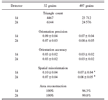
a Excluding 914 boundary triangles with misorientation >2°.
b Excluding 54 boundary triangles with misorientation >2°.
finds correct orientations and locates grain boundaries precisely. Table I indicates similar orientation noise for the two detector configurations.
The 497-grain data set again yields orientation noise on the order of 0.1° and reproduces the small grain shapes quite well. However, the misorientation plot in Figure 3b shows a significant number of triangles at grain boundaries that have been assigned the wrong orientation—in all cases, the assigned orientations are those of the neighboring grain. With g=6 triangles, the simulated microstructure’s side

Figure 5. (Color online) A stereographic projection showing the distribution of misorientation axes corresponding to the angles in Figure 4b. Axes were binned in 5°×5° boxes in the polar angles and the image has been symmetrized.
lengths are roughly twice the 1k×1k detector pixel size. Therefore, it is possible that when the collections of triangles that outline the simulated grains are projected onto the detector, the reduction to square pixilated data set leaves ambiguous regions in the microstructure where two orientations are possible. The higher resolution detector significantly improves this boundary precision problem: as indicated in the last entries in Table I, instead of 914 incorrect assignments there are only 54.
Table I gives some quantitative measures of the quality of the reconstructions. The triangle count indicates the effect of the adaptive regridding used in the 1k×1k fits. The effect is more dramatic with larger grains that have smaller perimeter to area ratios because boundary triangles are always regridded. Statistical measures are given comparing all four data sets: two input microstructures each reconstructed using two different detectors.
• Orientation precision is defined as the misorientation spread within reconstructed grains; numbers reported are the average and standard deviations over all grains. The measurement entails finding an average orientation for each grain and then calculating the misorientation between each constituent triangle composing the grain and this grain averaged orientation. Here, grains are identified as compact collections of triangles whose border elements have at least a 2° misorientation with their neighboring external triangles; this procedure is independent of the simulated microstructure and follows the grain identification procedure used with real experimental data. Orientation precision supplies an estimate of orientation noise intrinsic to the measurement and reconstruction as parametrized here. In real grains, orientation spreads larger than ∼0.1° should be observable. This number should be reducible by using smaller δ ω integration intervals and by fitting to intensity patterns within diffraction spots.
• Orientation accuracy is found by making a one-to-one correspondence between all reconstructed grains with all simulated grains. Here we calculate the misorientation between a reconstructed grain’s average orientation (Cho et al., Reference Cho, Rollett and Oh2004) and the orientation of its simulated counterpart. Unlike the precision, this is a macroscopic (rather than element-by-element) characterization.
• Spatial misorientation is found by regridding the reconstructed map so that all of its triangles exactly overlap one triangle in the input simulated structure and then calculating the misorientation between each overlapping triangle pair. The average misorientation between all triangles that have less than a 2° misorientation is quoted since this is how we previously defined our reconstructed grains. In the present case, the spatial misorientation is essentially the same as the precision; we include this statistic because it illustrates a method for comparing microstructures on a point-by-point basis, for example, before and after sample treatments.
• The percentage of the triangular elements containing less than 0.3° misorientation is listed as the area reconstruction. The deviation from 100% in the 497-grain simulation is due to incorrectly assigned boundary triangles.
CONCLUSION
We have verified the forward modeling technique of microstructure map generation using two sets of simulated data and two simulated experimental setups similar to configurations used at the APS 1-ID beamline. The ab initio orientation search identifies correct orientations within ∼0.1° misorientation for all tested cases. Grain geometries are reproduced to within detector resolution limits. These tests are, however, best case baseline scenarios. The reconstruction assumes perfect knowledge of the experimental geometry of the HEDM setup when in reality these parameters are determined with some finite uncertainty and imprecision. The simulated data set used an ideal microstructure with grains that contain no internal orientation variations. The detector images are noise-free. Further simulation tests are probing the effects of lifting these idealized conditions.
With the current reduction of experimental CCD images to binary data sets, the fitting is essentially attempting to pattern match the diffraction spot shapes that are projections of grain cross sections at multiple sample orientations, ω. The many projections of each grain provide some noise averaging, but confidence levels are typically reduced in the neighborhoods of grain boundaries (in experimental data sets). Fits to a variety of experimental data sets using the same algorithms as tested here have yielded complete orientation maps and statistical measures of microstructures consistent with electron backscatter diffraction (EBSD) volume measurements (Suter et al., Reference Suter, Hefferan, Li, Hennessy, Xiao, Lienert and Tieman2008; in progresswork). Experimental validations using measured data from test samples, including direct comparison to surface EBSD measurements, will also be published separately.
Further algorithm development is continuing. A major goal is to reduce computation time to be comparable to data collection speeds so that map output can be observed during data collection and used to guide further sample treatments and complimentary measurements. As a reference, the reconstructions presented here took on the order of 4 h on an 80-core parallel cluster, while acquisition of a comparable HEDM data set would require approximately 1 h. Intensity matching rather than binary pattern matching should lead to better sensitivity to intragrain orientation gradients. Inclusion of strain tensor parametrization in the scattering model will allow optimization of spatially resolved elastic strains within each triangle; experimental sensitivity to such strains will require modification of the experiment to include a “far-field” area detector that can resolve part in 104 motions of diffraction spots (Lienert et al., Reference Lienert, Brandes, Bernier, Weiss, Shastri, Mills and Miller2009). The overarching goal is to have a dedicated user facility at the APS that will be available and accessible to the materials community.
ACKNOWLEDGMENTS
We thank U. Lienert for his work in development of the experimental technique and its implementation at Sector 1 of the Advanced Photon Source. We have had helpful discussions with S. Garoff, G. S. Rohrer, A. D. Rollett, R. F. Sekerka, R. H. Swendsen, and M. Widom of Carnegie Mellon University and J. Sethna of Cornell University. This work was supported by the MRSEC program of the National Science Foundation under Award No. DMR-0520425 and NSF Metals program under Award No. DMR-0805100.


