


I. INTRODUCTION
Active electronically scanned array (AESA) radars are increasingly being favored over conventional mechanically scanned systems. The achievable radar range of such an AESA radar is mainly determined by the output power and the noise figure of the antenna. Both properties can be improved using GaN technology. T/R modules are key elements in active phased-array antennas for radar and electronic warfare applications [Reference Holpp and Worning1]. Inside these T/R modules two main building blocks are the amplifier chain in the transmit path and the low noise amplifier (LNA) in the receive path.
In most of today's T/R modules GaAs monolithically integrated circuit (MMIC) amplifiers are used with typical output power levels in the range of 5–10 W [Reference Mancuso, Gremillet and Lacomme2–Reference Kopp, Borkowski and Jerinic4]. Higher output power levels, broader bandwidth, increased power-added efficiency (PAE) values, and higher operating voltages are advantages for performance improvement to meet future requirements. For these applications the use of amplifiers based on AlGaN/GaN is a very promising approach [Reference Kinghorn5–Reference Sheppard8]. With the GaN technology, high-power amplifiers (HPAs) with higher output power compared to GaAs MMICs are already demonstrated [Reference Costrini9–Reference Piotrowicz, Morvan and Aubry11]. With limited prime power and also limited cooling capacity, as often existing in military systems, another important parameter is the PAE of the amplifier. Due to the higher breakdown voltage of the GaN device compared to a GaAs device, the supply voltage can be significantly increased. This leads to an additional increase in efficiency on system level, because of lower losses in the power supply.
Besides the noise figure performance the robustness against high input power overdrive is also a key issue for the receive path in a T/R module. The AlGaN/GaN technology with its high breakdown voltage is very well suited for robust low noise applications [Reference Schwindt, Kumar, Aktas, Lee and Adesida12,Reference Janssen, van Heijningen, Provenzano, Visser, Morvan and van Vliet13].
To satisfy these future needs, a T/R-module front-end composed of novel GaN MMICs and multi-layer packaging technology is designed.
In this paper the design and the achieved performance of single GaN MMIC amplifiers and of a whole T/R-module front-end based on these GaN MMICs are presented.
The MMIC and front-end design, simulation, and measurements are performed at European Aeronautic Defence and Space (EADS) Defence Electronics, Ulm. The wafer and MMIC fabrication is done at the Fraunhofer Institute of Applied Solid-State Physics, Freiburg.
II. GaN MMIC TECHNOLOGY AND MODELING
The AlGaN/GaN HEMT MMIC technology is based on multi-wafer growth of single heterojunction devices on 3-in s.i. SiC substrates by metal organic chemical vapor deposition (MOCVD). The 3-in HEMT technology uses electron-beam-defined gates with 0.25-µm gate-length including fieldplates for high-power operation.
The two-terminal breakdown voltages of the power HEMTs are BV > 100 V. Typical output power densities are beyond 5 W/mm at 10 GHz with an associated drain efficiency η > 50% at V DS = 28 V for high efficiency operation. For low-noise operation, the AlGaN/GaN HEMTs yield a minimum noise figure of NF < 0.8 dB at f = 10 GHz and V DS = 10 V.
After the front side processing, the full 3-in SiC wafer is thinned to 100 µm thickness and a via-hole back side process is applied. In Fig. 1 photo of the cross-section is shown. The via-holes are well covered by metal from the back side, which ensures good grounding of the front side elements.

Fig. 1. Photo of the cross-section of a 100-µm-thick SiC wafer substrate, with a HEMT structure on the front side, via-holes, and back side metallization.
For the design a library of passive microstrip components is available, including all technology-specific elements like capacitors, resistors, and inductances. The large-signal GaN HEMT modeling is based on an in-house two-dimensional voltage-lag model to appropriately describe thermal effects and low-frequency dispersion, and their impact on gain and PAE [Reference Seelmann-Eggebert, Merkle, van Raay, Quay and Schlechtweg14].
III. DRIVER AMPLIFIER MMIC
The MMIC driver amplifier (DA) is designed as a two-stage amplifier with one transistor 8 × 60 µm gate-finger width in the first stage and one transistor 8 × 125 µm gate-finger width in the second stage (see Fig. 2). The amplifier is designed for an impedance of 50 ohm at the input and output ports and for operation in linear mode, not using the whole available output power of the transistor. One design objective was to provide enough input power for two HPAs in parallel configuration in the frequency band from 8 to 12 GHz. Although this amplifier will be used for operation in linear mode, the output matching is designed using harmonic balance simulation.

Fig. 2. Photo of a GaN DA MMIC chip. Chip size: 3 mm × 2 mm.
In Fig. 3 a whole wafer mapping of the measured small signal gain is shown. Comparing the simulated small signal gain at V DS = 15 V with the on-wafer measurements, a very good compliance is observed. The uniformity is very good over the entire 3-in wafer.

Fig. 3. Measured on-wafer small signal gain versus frequency of the GaN DA MMIC at V DS = 15 V compared with the simulated performance.
The maximum measured output power is higher than 38 dBm while operating in saturation mode with up to 5-dB gain compression (Fig. 4). This output power leads to a power density of 7.4 W/mm at the transistor level. The measured saturated output power is even a little bit higher than that predicted by the simulation. The achieved output power is sufficient for driving one or two HPAs in the frequency range between 8.5 and 14 GHz, while operating the DA below the 1-dB compression point.

Fig. 4. Comparison of the simulated and measured output power versus frequency of the GaN DA MMIC at 1 dB gain compression and at saturation with V DS = 30 V and V GS = −4.9 V.
IV. HIGH-POWER AMPLIFIER MMIC
The MMIC HPA is designed as a two-stage amplifier based on four transistors with 8 × 125 µm gate-finger width in the second stage and two transistors with the same size in the first stage (see Fig. 5). The amplifier is designed for an impedance of 50 ohm at input and output ports. The output combiner is optimized for maximum output power in the frequency range from 8.5 to 11 GHz.
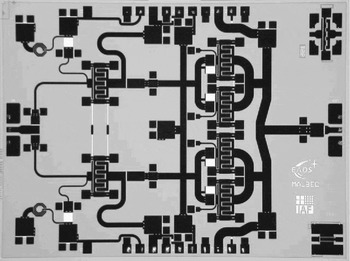
Fig. 5. Photo of a GaN HPA MMIC chip. Chip size: 4 mm × 3 mm.
Previous intensive load-pull simulations have been performed to find the optimum load impedance for maximum output power.
For electrical stabilization of the second-stage RC networks close to all transistor inputs are used. Odd-mode stability analysis has been performed for the parallel transistor structure. The first-stage transistors are stabilized by the gate bias circuits. The interstage network and the output combiner are optimized by electromagnetic simulations of distributed elements. An improved PAE performance is obtained by the application of second harmonic short networks at all gates of the second-stage transistors.
The on-wafer measurement of the small signal gain is indicating a slightly higher slope in the frequency range from 8 to 10 GHz compared to the result obtained by simulation (see Fig. 6). The uniformity over the entire wafer is again very good. The output power, gain, and PAE measurement results in pulsed mode are shown in Fig. 7.

Fig. 6. Measured on-wafer small signal gain versus frequency of the GaN HPA MMIC at V DS = 15 V compared with the simulated performance.

Fig. 7. Measured power performance of the GaN HPA MMIC at 11 GHz with V DS = 30 V and V GS = −5 V. P max = 43 dBm and PAE max = 31%.
Here, pulse conditions with 50 µs pulse length and 10% duty cycle are used for all pulsed measurements. The maximum measured output power is 20 W, when biased for class-AB operation. This output power leads to a power density of 5.7 W/mm at the transistor level. In this case the small signal gain is about 18 dB and the associated PAE value is 31%.
The small signal gain at V DS = 30 V is higher than 15 dB over the whole frequency range from 8.5 to 11 GHz (see Fig. 8). The simulated small signal gain is more flat for lower frequencies, as already seen when operating the HPA with V DS = 15 V. A part of the measured slope is linked to a weak input matching at frequencies around 8.5 GHz. More than 14 W output power is measured over a frequency range from 8.75 to 11.5 GHz. Again the simulated output power fits very well with the measurement results.

Fig. 8. Comparison of the simulated and measured saturated output power and small signal gain versus frequency of the GaN HPA MMIC. Bias point: V DS = 30 V and V GS = −5.0 V.
V. LOW-NOISE AMPLIFIER MMIC
For the designed MMIC LNA the same transistor size of 8 × 30 µm is used for the first and second stage (see Fig. 9). For this first iteration design the transistor layout was not optimized for low-noise operation. It is similar to the power transistor layout. The transistor size of the first stage is a trade-off between low-noise performance and large signal robustness.

Fig. 9. Photo of a GaN LNA MMIC chip. Chip size: 3 mm × 2 mm.
To allow a simultaneous noise match and input match over a sufficiently broad bandwidth, an additional source inductance is used. The design model is based on small signal and noise parameter measurements of the transistor, without any inductive feedback.
For decoupling purpose, but also to increase the robustness [Reference Rudolph15], a resistor is used in the gate bias network. This LNA MMIC was originally designed for transistors with shorter gate length for the frequency range from 8 to 12 GHz [Reference Schuh16]. Using a new transistor geometry a shift to lower frequencies occurred.
Taking into account the new transistor model a gain between 15 and 17 dB is simulated in the frequency range from 6.5 to 10 GHz. The expected noise figure is about 1.5 dB.
Again a very good agreement between simulation and measurement of the small signal gain exists (see Fig. 10). The shape of the frequency response is well predicted through the simulation. The average measured gain is about 1 dB higher than the simulated gain.

Fig. 10. Measured on-wafer small signal gain versus frequency of the GaN LNA MMIC at V DS = 15 V compared with the simulated performance.
In Fig. 11 the simulated and measured noise figure of the GaN LNA MMIC is shown. The obtained noise figure is very close to the expected one over the whole frequency band. The minimum noise figure is only about 1.45 dB. For frequencies up to 10.5 GHz the noise figure of this GaN LNA is only 0.5 dB worse than the normally used GaAs LNA [Reference Feldle and Reber17].

Fig. 11. Comparison of the simulated and measured gain and noise figure versus frequency of the GaN LNA MMIC with V DS = 15 V and V GS = −2.2 V. NF min = 1.45 dBm.
Besides the good noise performance the behavior of LNA with large input power signals is very important for this type of LNA. The saturated output power of the LNA is about 26.5 dBm (see Fig. 12). First robustness tests have been performed up to 6 W input power. At this input power level the LNA is about 27 dB in compression.

Fig. 12. Measured output power and gate current versus input power of the GaN LNA MMIC. Bias Point: V DS = 15 V and V GS = −2.2 V.
VI. T/R-MODULE FRONT-END
For the front-end a multi-layer low-temperature cofired ceramic (LTCC) substrate is used. After obtaining first experience with an amplifier chain on LTCC with GaN MMICs [Reference Feldle and Reber17] some modifications are realized. In Fig. 13 the completely assembled new front-end is shown.

Fig. 13. Photo of a T/R-module front-end with GaN MMIC chips.
One big challenge is the thermal situation with these GaN MMICs having a very high-power density compared to today's state-of-the-art GaAs MMICs.
A first approach was to use AlN high-temperature cofired ceramic (HTCC) instead of LTCC because of its significantly higher thermal conductivity. In this case the DA and the two HPAs were mounted directly on the HTCC substrate in cavities. In Fig. 14 thermal photos of the GaN MMICs are shown. During the measurement the same dissipation power was used for both assemblies, the LTCC version (Fig. 14(a)) and the HTCC version (Fig. 14(b)). When mounting the DA on top of the HTCC substrate, the thermal situation is improved. The thermal conductivity of HTCC is much higher than the thermal conductivity of LTCC with thermal via-holes. But the situation is changing in the case of HPAs. The thermal situation is dramatically declined compared to the LTCC version where the HPAs are mounted on a metallic heatsink.

Fig. 14. Thermal photos of the GaN MMIC mounted on different substrates. Brighter colors represent higher temperature: (a) LTCC and (b) HTCC.
The favored solution today is using the proven LTCC technology for T/R modules used in series production and soldering the DA similar to the HPAs on a CuMo heatsink.
The T/R module front-end consists of a whole transmit path with one DA and two HPAs in parallel, a circulator, a receive path with LNA and limiter and a GaAs switch combining both paths. It can be used as a front-end for a software-defined radar or can be combined with any core chip using CMOS, SiGe, or GaAs technology.
Besides the RF relevant components, like power splitter and combiner, also the whole DC control electronics is integrated on the substrate. The control electronics provides the pulsed 30v drain voltage for the GaN high-power MMICs, the LNA bias voltages, and the T/R switch control.
For the transmit operation mode the output power, gain, and PAE measurement results in pulsed mode are shown in Fig. 15. The maximum measured output power is 32 W. In this case the small signal gain is about 31 dB and the associated front-end PAE value is 24%, also taking into account the dissipation power of the control electronics.

Fig. 15. Measured power performance of the GaN T/R-module front-end at 11 GHz with V DS = 30 V and V GS = −5 V. P max = 45 dBm, PAE max = 24%.
More than 20 W output power is measured over a bandwidth of 2.5 GHz (see Fig. 16). The small signal gain of the front-end has a positive slope versus frequency up to 11 GHz.

Fig. 16. Measured saturated output power and small signal gain versus frequency of the GaN T/R-module front-end. Bias point: V DS = 30 V and V GS = −5.0 V.
In the receive operation mode a small signal gain in the range of 12.5 dB is measured. The associated noise figure is about 2 dB at room temperature (see Fig. 17). After the initial noise figure measurement the input power at the front-end was stepwise increased up to 7 W. After each step the noise figure measurement was repeated. In Fig. 17 the noise figure measurement result after applying 7 W input power is the same just like the initial measurement result. Also there is no variation of the receive gain visible.

Fig. 17. Measured gain and noise figure versus frequency of the GaN T/R module front-end. Initial measurements (solid lines) and after applying 7 W input power (dashed lines). NF min = 2 dBm.
In Fig. 18 the compressed output power of the front-end in receive mode is shown. Up to 7 W input power the output power stays below 8 dBm. This allows a safe operation of the following small signal MMICs like GaAs core chips.

Fig. 18. Measured output power and gate current versus input power of the GaN T/R-module front-end in the receive mode.
VII. CONCLUSION
A whole GaN MMIC amplifier chip set for an X-band T/R module front-end was designed, simulated, fabricated, and measured. Output power levels up to 20 W for the transmit path HPA and a noise figure of 1.45 dB for the receive path LNA are achieved. A T/R module front-end with three types of amplifiers (DA, HPA, and LNA) integrated on multi-layer LTCC substrates is successfully demonstrated. To our knowledge, this is the first published GaN-based T/R module front-end, outperforming the state-of-the-art GaAs-based T/R module front-end in terms of transmit output power and receive noise figure. With such a front-end, T/R modules with more than 20 W transmit output power and a receive noise figure below 3 dB can be realized.
ACKNOWLEDGEMENTS
This work was partly funded by the German Bundeswehr Technical Center for Information Technology and Electronics (WTD81), Greding, and the German Federal Ministry of Defence (BMVg), Bonn. This financial support is gratefully acknowledged. The authors thank Wolfgang Brommer and the IAF clean room personnel for their strong support.
 Patrick Schuh received the Dipl-Ing. degree and the Dr.-Ing. degree in electrical engineering from the University of Ulm, Ulm, Germany, in 1998 and 2003, respectively, and the Masters degree in business administration from the University of Applied Sciences Neu-Ulm, Neu-Ulm, Germany, in 2004. From 1998 to 2002 he was a Research Assistant with the Microwave Techniques Department, University of Ulm, where he was involved with the analysis and the design of packages for microwave applications, utilizing electromagnetic simulations. From 2002 he has been with the European Aeronautic Defence and Space (EADS) Company Deutschland GmbH, Defence Electronics, Ulm, Germany. From 2009 he is heading the GaN and SiGe group inside the “MMICs and T/R modules” department. His current area of interest is MMIC and T/R-module design, especially high-power amplifiers in GaN and GaAs technology. He is a member of IEEE, MTT.
 Hardy Sledzik was born in Oberhausen, Germany, in 1959. He received the Dipl.-Ing. degree and the Dr.-Ing. degree in electrical engineering from the University of Duisburg, Duisburg, Germany, in 1986 and 1990, respectively. From 1986 to 1990, he was a research assistant at the Institute of Electromagnetic Theory and Engineering, University of Duisburg. From 1990, he has been with EADS Deutschland GmbH, Defence Electronics, Ulm, Germany. His current area of interest is high-power amplifier design, in GaN and GaAs technology.
 Rolf Reber received his Diplomingenieur's degree from the University of Karlsruhe, Germany. He joined the Radar Group of AEG-Telefunken Ulm/Germany (which is now part of EADS) in 1987, where he has been engaged in the design and development of microwave components for active phased-array antennas. His current work includes the development and design of MMICs in GaAs- and GaN-technology dedicated for T/R modules and the research in the field of modern amplifier topologies for wireless communication.
 Andreas Fleckenstein received the diploma degree in electrical engineering and communication technology from Technische Universität Darmstadt, Germany, in 2003. He is currently working toward the doctoral degree of Ulm University, Ulm, Germany. During his studies he was engaged in several antenna topics at the DaimlerChrysler research center in Ulm. In 2004 he joined the Ulm University Institute of Microwave Techniques as research assistant. There he studied advanced packaging concepts for microwave components in cellular phones. Since end of 2007 he is with EADS Deutschland GmbH in Ulm. His current research interest is focused on T/R-module design – especially for space applications. He is a member of IEEE.
 Ralf Leberer was born in Tettnang, Germany, in 1973. He received his master degree in electrical engineering in 1999 and the doctorate in 2005 from the University of Ulm, Germany. In the department of microwave techniques at the University of Ulm, his research interests were on quasi-planar reflector antennas for communication systems. He joined EADS Deutschland GmbH in 2005. During the time at the department for MMICs and T/R modules he specialized in power amplifier design and GaN-technology. He is the author of more than 20 publications. His current research interests are high efficient high linear power amplifiers for communication, GaN technology, and T/R modules for radar. He is a member of IEEE and has received several local or international prizes like the European Microwave Prize.
 Martin Oppermann was born in Cologne (Germany) in 1960. He holds a diploma degree and a doctor's degree in physics from the University of Tübingen. In the Department of Applied Physics and in the Natural and Medical Science Institute (NMI) his research activities were in semiconductor electronics and thin film technologies for application in optics and electronics. After 2 years of semiconductor processing and engineering with the BOSCH company in Reutlingen he started 1993 inside EADS in the department of RF (is part of the department name) module development and ceramic substrates. As an expert of module technologies he focused on mm- and microwave-qualified substrate and assembly technologies. In 2007 he became the head of the department of “T/R modules and MMICs”. He is a member of the DPG (German Physical Society) and an international member of International Microelectronics and Packaging Society (IMAPS).
 Rüdiger Quay received the Diplom degree in physics from Rheinisch-Westfälische Technische Hochschule (RWTH), Aachen, Germany, in 1997, and a second Diplom in economics in 2003. He received his doctoral degree in technical sciences (with honors) from the Technische Universität Wien, Vienna, Austria. He is currently a research engineer with the Fraunhofer Institute of Applied Solid-State Physics, Freiburg, Germany, heading the RF-devices and characterization group. He has authored and coauthored over 75 refereed publications and three monographs. He is a member of IEEE; MTT, VDE; VDI, and MTT-6.
 Friedbert van Raay was born in Hilden, Germany, in 1960. He received an M.Sc. degree in electrical engineering from Technical University of Aachen, Germany, in 1984, and a Ph.D. degree from the University of Kassel in 1990. From 1992 to 1995, he was with the SICAN GmbH, Hannover, Germany, working on RF system development and measurement techniques. In 1995, he returned to the University of Kassel as a senior engineer. He supervised the Microwave Group within the Institute of High Frequency Engineering and worked on design of ultra-broadband GaAs MMICs, device modeling and large-signal measurement techniques. In November 2001, he joined the Fraunhofer Institute of Applied Solid-State Physics in Freiburg, Germany. His research interests include MMIC design, device modeling, and measurement techniques.
 Matthias Seelmann-Eggebert received his diploma and a Ph.D. degree in physics from the University of Tübingen in 1980 and 1986, respectively. From 1980 to 1996 he was involved in R&D related to infrared detectors based on HgCdTe and developed electrochemical and surface physical methods for the characterization of compound semiconductor surfaces. From 1990 to 1991 he was a visiting scientist at Stanford University. From 1997 to 2000 he was engaged in the growth of CVD diamond. From 2001 he is a member of the Department of High Frequency Electronics of the IAF in Freiburg, Germany, and is concerned with the preparation and development of simulation models for active and passive III–V devices.
 Rudolf Kiefer received his Dip. Phys. degree in physics from the University of Freiburg, in 1979. He joined the Fraunhofer Institute of Applied Solid State Physics (IAF) in 1980 starting work on liquid crystal displays. For work on this topic he received a Ph.D. degree in physics in 1984 from the University of Freiburg. From 1984 to 1991 he investigated electro-optic effects in ferroelectric, liquid crystalline polymeric materials for optical storage applications. Afterwards he focused his work on studying a new switching effect of nematic liquid crystals to improve the viewing angle characteristics of thin film addressed liquid crystal displays (TFT-LCD). For this work he received a SID Award in 1998. In 1994 he moved to the field of III-V optoelectronic semiconductor technology. He managed different technology projects developing processes for fabrication and laser facet deposition of InP-based high-speed laser and GaAs as well as GaSb-based high-power laser. From 2000 his work is focused on the development of GaN semiconductor technology for MMICs.
 Michael Mikulla received his diploma degree in electrical engineering from the Technical University of Braunschweig, Germany, in 1989 and a Ph.D. degree from the University of Ulm, Germany, in 1994. From 1994 he has been with Fraunhofer IAF in Freiburg, Germany, working on both high-power semiconductor lasers and GaN-based high-power transistors and MMICs. He has authored and has published over 100 conference/journal papers. From 2002 he is the head of the III/V-Technology department of the institute and is also in charge of the GaN RF Power Electronics business unit.


