I. INTRODUCTION
Reception Systems for Direct Broadcast from Satellite (DBS) require low-profile, compact antenna systems for automotive use. High-efficiency antenna arrays are particularly important for these applications. Low-profile antenna designs have been proposed in the past but most of them were fairly narrowband and limited to maximum 500 MHz bandwidth [Reference Ito and Yamazaki1–Reference Shahabadi, Busuioc, Borji and Safavi-Naeini6]. Wideband antenna array that can cover entire Ku-band downlink frequency band (10.8–12.75 GHz) was presented in [Reference Bilgic and Yegin7] for a fixed beam tilt array. In this study, we propose a compact, wideband planar array that has high aperture efficiency due to low-loss feed network for automotive applications of satellite TV reception.
Satellite tracking on a mobile platform can become difficult if the system cost needs to be very low for high-volume manufacturing. Thus, electronic scanning in both azimuth and elevation axis is not preferred due to the cost involved in incorporating high number of phase shifters required for beam pointing. Instead, azimuth scanning with mechanical rotation and elevation scanning over a relatively small range of angles are usually implemented. The antenna often has a fixed elevation tilt or mechanical tilt toward desired satellite transponder and small number of phase shifters maintains the beam at desired position, which changes due to dynamic driving conditions.
Typical DBS reception antennas require at least 28 dBi gain to meet gain-over-temperature (G/T) criterion for minimum carrier-to-noise ratio (CNR). However, antennas meet such requirement are excessively large (at least 1 m in diameter) for automotive use. Instead, 24–25 dBi gain antenna arrays that specifically target certain channels where signal strength is relatively strong are envisioned for automotive applications. To receive signal from multiple transponders, the antenna array must be wideband. Therefore, requirements for automotive use demand compact, low-profile, high-gain (high-efficiency), and wideband antenna array. The proposed antenna in this study satisfies all these requirements, and to keep the dimensions low single polarization (vertical) panel is designed. To increase the efficiency of the antenna, planar microstrip patch array is combined with a waveguide feed network. Contrary to earlier hybrid feed networks [Reference Shahabadi, Busuioc, Borji and Safavi-Naeini6, Reference Bilgic and Yegin7], we propose a low-loss microstrip-to-waveguide transition and we validate the results with feed network prototypes. CNR measurements of the antenna reveal good reception.
II. ANTENNA ELEMENT DESIGN
The directivity of TM01 mode broadside patch is roughly:
 $${D_p}=\displaystyle{{4\pi } \over {{\Omega _A}}} \approx \displaystyle{{4\pi } \over \pi }=4\, \lpar 6\, {\rm dBi}\rpar \comma \;$$
where, ΩA represents the beam solid area. For K elements, array directivity D A becomes:
 $${D_A} \approx K{D_p}.$$
If elevation scanning of ±15° is assumed, half-power beamwidth in elevation (HPBW θ) in elevation can be taken as 30°. Also, HPBW ϕ can be set to 6° for azimuth tracking since geostationary satellites are mostly positioned 6° or more apart. Then, the directivity of the array is roughly:
 $${D_A} \approx \displaystyle{{40000} \over {HPB{W_\theta }HPB{W_\phi }}} \approx 222.2\lpar 23.47\, {\rm dBi}\rpar.$$
Furthermore, if 60% total efficiency (due to feed network loss, mismatch loss) is assumed, the gain of the array should be 370 (25.6 dBi). Number of broadside patch elements required for this gain is 62. To preserve symmetry, 64-element array is taken as the starting point using above rough estimate of antenna array gain.
To meet bandwidth requirements of the array antenna, the element antenna should possess even broader bandwidth than the array. Although feed network loss indirectly improves impedance match of the array, inter element coupling reduces single antenna bandwidth. Non-resonant slot coupled stacked patch antenna was shown to exhibit very good bandwidth and gain characteristics at this frequency band [Reference Bilgic and Yegin8]. Similar but different element antenna configuration is shown in Fig. 1. Equivalent circuit model of the slot coupled patch with parasitic element is illustrated in Fig. 2.

Fig. 1. Nonresonant slot coupled patch antenna configuration (h 1 = 1 mm, h 2 = 3, h 3 = 5.8 mm, L RP = 10.8 mm, L PP = 9.3 mm, S PP = 1.5 mm, S RP = 1.7 mm, and W Feed = 1.1 mm).
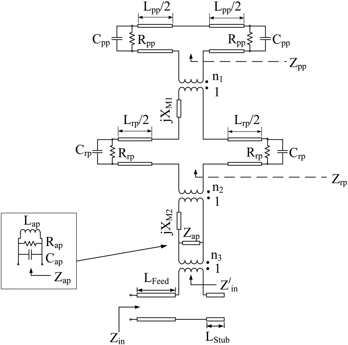
Fig. 2. Equivalent circuit model of slot coupled patch with parasitic element.
Capacitive coupling between the patches and patch-to-ground are stated in terms of jX M1 and jX M2, respectively. The input impedance of the circuit can be derived as:
 $$\eqalign{{Z_{in}}={Z_0}\cr & \displaystyle{{Z_{in}^{\prime}+j{Z_0}\tan \, \lpar {\beta _{eff}}{L_{stub}}\rpar +j{Z_0}\tan \, \lpar {\beta _{eff}}{L_{feed}}\rpar } \over {{Z_0}+jZ_{in}^{\prime} \tan \, \lpar {\beta _{eff}}{L_{feed}}\rpar +j{Z_0}\tan \, \lpar {\beta _{eff}}{L_{stub}}\rpar \tan \, \lpar {\beta _{eff}}{L_{feed}}\rpar }}\comma}\;$$
where β eff is calculated using effective dielectric constant of the substrate material and Z ′in is given by:
 $$Z_{_{in} }^{\prime}={Z_1}/{Z_2}$$
with
 $${Z_1}={Z_{ap}}{Z_{rp}}\lpar n_1^2 {Z_{M1}}+{Z_{pp}}\rpar +{\lpar {n_1}{n_2}\rpar ^2}{Z_{ap}}{Z_{M2}}\lpar {Z_{rp}}+{Z_{M1}}\rpar +n_2^2 {Z_{pp}}{Z_{ap}}{Z_{M2}}$$
and
 $${Z_2}=n_3^2 {Z_{rp}}\lpar n_1^2 {Z_{M1}}+{Z_{pp}}\rpar +{\lpar {n_1}{n_2}{n_3}\rpar ^2}\lpar {Z_{rp}}+{Z_{M1}}\rpar \lpar {Z_{M2}}+{Z_{ap}}\rpar +{\lpar {n_2}{n_3}\rpar ^2}{Z_{pp}}\lpar {Z_{M2}}+{Z_{ap}}\rpar \comma \; $$
where Z ap, Z rp, Z pp, Z M1, Z M2, n 1, n 2, and n 3 can be calculated using relations in [Reference Edimo, Mahdjoubi, Sharaiha and Terret9–Reference Pues and Van de Capelle11].
Although it is difficult to infer the role of parasitic patch from (5) to (7), its presence greatly improves the bandwidth and slightly increases gain when compared with without parasitic configuration. Square patch with corners cut is used because this type of patch was found to produce less mutual coupling in the array configuration through numerical simulations. Reflector ground that is quarter wavelength away from feedline is used to minimize backside radiation and to provide shielding for the feed network. Patch elements were etched on thin film with 75 µm thickness and Rohacell HF31 foam (ε r = 1.046, tanδ = 0.0017) was used as air dielectric. Feedline substrate was Nelco NX9300 (ε r = 3 and tanδ = 0.0013) with 0.5 mm thickness. Measured input impedance match and broadside gain of the element antenna are shown in Fig. 3. Impedance match (|S 11| < −9.5 dB) is from 10.3 to 13.7 GHz with 25% bandwidth. Broadside gain of the antenna within the downlink of Ku band is above 8.9 dBi and HPBW θ is 80° throughout the frequency band.
Fig. 3. Measured gain and input match of aperture coupled antenna (![]() Measured Input Reflection Coefficient,
Measured Input Reflection Coefficient, ![]() Measured Gain).
Measured Gain).
III. SUBARRAY DESIGN
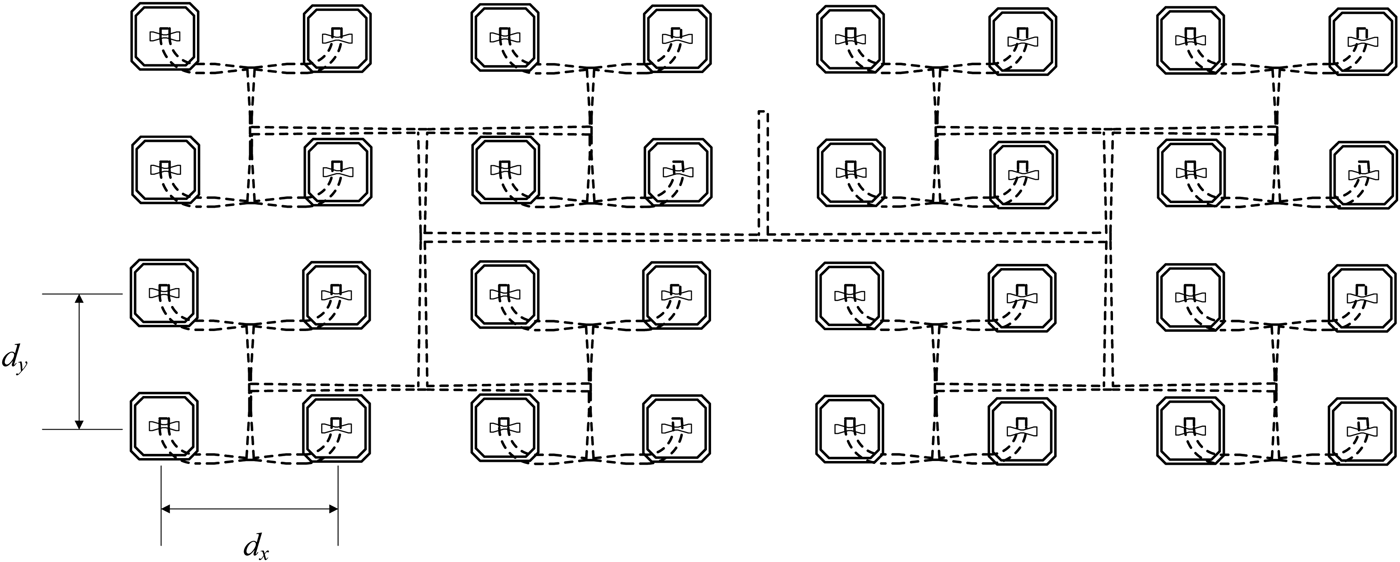
The array antenna is formed by two subarrays and each subarray consists of 32 elements. The antenna is designed for single polarization only and vertical polarization is chosen for the implementation. However, dual polarization can also be designed using a different panel for the horizontal polarization. Subarray design with its microstrip feed network is shown in Fig. 4. T-junction equal power dividers were optimized for impedance match, power division, and phase balance using AWR Microwave Office. Simulated antenna impedance of each element in the subarray is used as the terminating impedance on the feed network design. Simulations of the antenna were performed using FEKO, three-dimensional (3D) electromagnetics field solver based on the Method of Moments. Simulated and measured gain and input impedance match of the subarray are shown in Fig. 5. Measured match is better than −10 dB throughout the Ku-band downlink band and in-band worst broadside gain is 21.2 dBi. Maximum discrepancy between the simulated and measured gains is about 0.8 dB, which is fairly acceptable considering that the feed connector was not taken into account in the simulations.
Fig. 4. Subarray with feed network. (d x = d y = 22 mm)
Fig. 5. Subarray gain and input match (![]() Measured gain,
Measured gain, ![]() Simulated gain,
Simulated gain, ![]() Measured S11,
Measured S11, ![]() Simulated S11)
Simulated S11)
Normalized antenna patterns for the subarray are shown in Fig. 6. HPBW in azimuth and elevation are 8° and 14°, respectively.
Fig. 6. Normalized gain patterns of the subarray: (a) azimuth, (b) elevation (![]() Measured,
Measured, ![]() Simulated).
Simulated).
IV. FEED NETWORK DESIGN
Microstrip feed network loss can be prohibitively large for arrays at these frequencies. For a 64-element array, the total microstrip feedline length for a corporate feed becomes approximately 274 mm which leads to about 2.8 dB feed network loss using the substrate material and thickness mentioned in Section II. Microstrip feed network loss for 32-and 64-element arrays excluding the connector losses are shown in Fig. 7. To minimize feed network loss, waveguide feed network is used to combine two subarrays. Thus, the feed network is a hybrid of microstrip and waveguide combiners. Loss in the waveguide feed network is much smaller than its microstrip counterpart, but microstrip to waveguide transition can be high if not designed properly.
Fig. 7. Microstrip feed network loss. (![]() 32 element array,
32 element array, ![]() 64 element array).
64 element array).
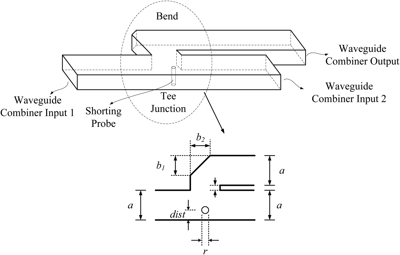
The 2:1 waveguide combiner is shown in Fig. 8. H-type waveguide combiner as opposed to an E-type combiner was used. With H-type combiner, the electric field lines are parallel to the longitudinal axis of the guide and the height of the waveguide can be reduced by half which brings a significant height advantage. Also, output ports are in phase and no phase compensation is needed. T-junction bents and shorting post were carefully designed for wideband impedance match. Simulation of the waveguide combiner for surface currents is shown in Fig. 9.
Fig. 8. Waveguide combiner (a = 18.85, b = 4.75, b 1 = b 2 = 5.2, dist = 3.4, r = 1, all in mm).
Fig. 9. Simulation of surface currents for waveguide combiner.
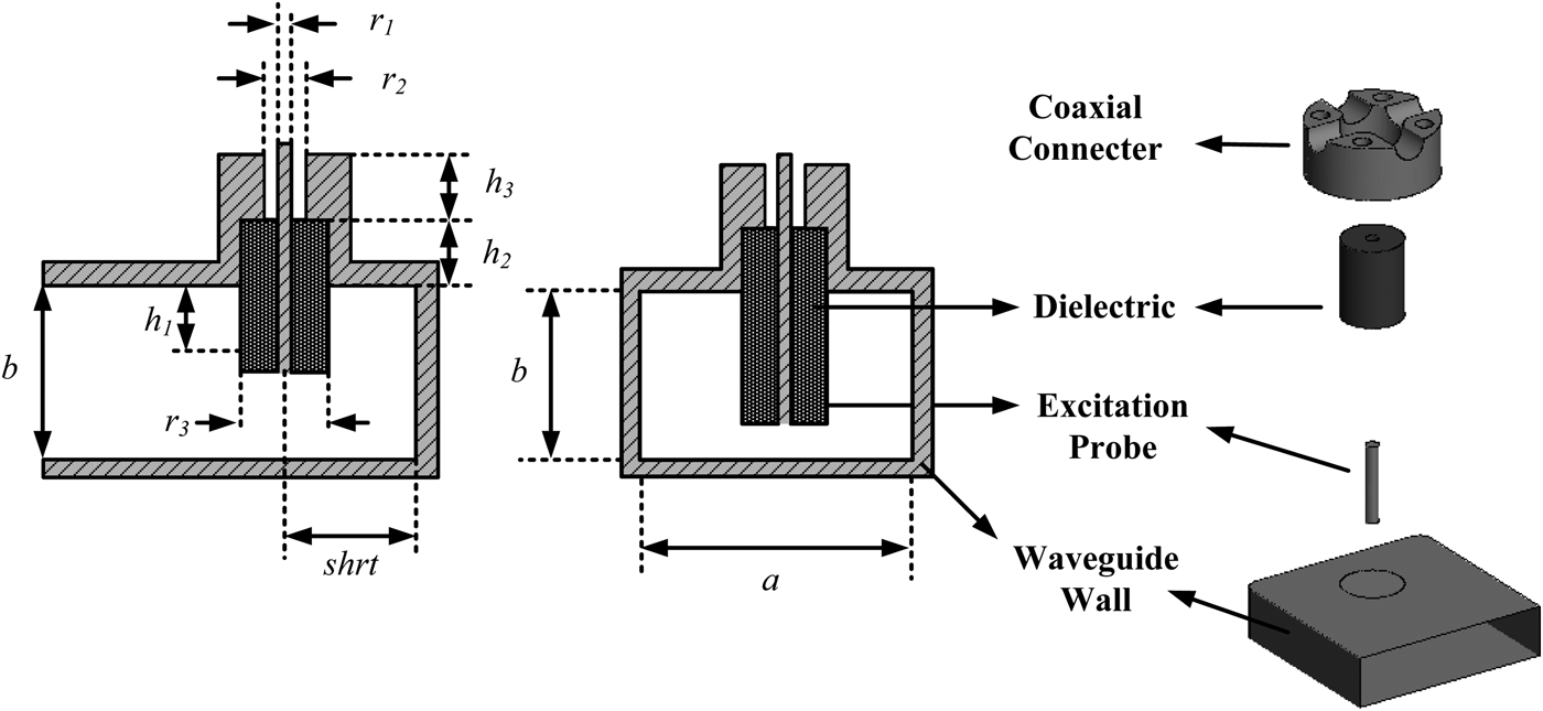
Microstrip-to-waveguide junction is a crucial part of the design as its loss can be detrimental on array performance. Dielectric-loaded probe transition is designed and verified using CST Microwave studio. It is observed that this transition has lower loss than the disc-loaded transition used in [Reference Bilgic and Yegin7]. Disc-loaded feed presented capacitive loading to the pin, whereas dielectric loading acted as an inductive loading to the pin. Although capacitive loading is known to provide better impedance bandwidth, inductive loading resulted in lower loss in the present design. Rexolite 1422 (ε r = 2.53, tanδ = 0.0001) was used as the dielectric material. The configuration of the transition is displayed in Fig. 10. To assess the transition and the waveguide loss, prototypes of the waveguide combiner, and transitions were made. Waveguide combiner was micromachined from aluminum alloy cast and shown in Fig. 11. Also, a Wilkinson power divider using microstrip lines was made. The outputs of Wilkinson power divider were connected to the microstrip-to-waveguide transitions and the output of the waveguide is connected to a coaxial probe using the same transition as shown in Fig. 12. To eliminate the loss incurred by the Wilkinson power divider and output coaxial cable, an identical Wilkinson divider followed by the same type combiner was also made. That way, input and output measurements of the two Wilkinson dividers/combiners could be made. Measured transition and waveguide loss are shown in Fig. 13. The impedance match looking from output is also shown in Fig. 13.
Fig. 10. Microstrip to waveguide transition (a = 18.85, b = 4.75, shrt = 7.2, r 1 = 1, r 2 = 1.62, r 3 = 5.6, h 1 = 3, h 2 = 2, h 3 = 5.5, all in mm).
Fig. 11. Waveguide combiner prototype.
Fig. 12. Wilkinson power divider on the inputs of waveguide combiner.
Fig. 13. Measured transition and waveguide loss.
V. FULL ARRAY DESIGN
Two subarrays combined with waveguide feed network constitute 64-element array antenna. The array prototype is shown in Fig. 14. The output port is transitioned to WR75 waveguide port for low-noise block (LNB) connection for measurements and satellite reception tests. Beam tilt along elevation axis is achieved by mechanical tilt, which increases the overall height of the array according to:
 $$h=W\, {\rm sin}\, {\rm \Psi\comma \; }$$
where Ψ is the mechanical tilt angle and W is the width of the array. The array takes up less than 18 cm diameter in transverse dimensions and 5.5 cm in height for a transponder at 40°.
Fig. 14. Prototype of the array (L = 176, W = 86 mm).
Gain and input match of the array are shown in Fig. 15. Simulated and measured gain agrees well except toward the end of downlink band which was mainly due to microstrip-to-waveguide transition loss. Maximum and average measured broadside gains of the antenna are 25 and 24.1 dBi, respectively. Its measured input match is below −9.5 dB. Measured gain patterns (at 11.9 GHz) along the azimuth and elevation axis are shown in Fig. 16. HPBW θ and HPBW ϕ are 14° and 4.5°, respectively. The elevation HPBW remains unchanged when compared with that of the 32-element subarray since no additional elements are added in that direction. The antenna achieves mostly above 61% aperture efficiency up to 12.2 GHz and 71% aperture efficiency at 11.1 GHz.
Fig. 15. Array gain and input match (![]() Measured Gain,
Measured Gain, ![]() Simulated Gain,
Simulated Gain, ![]() Measured Input Match,
Measured Input Match, ![]() Simulated Input Match).
Simulated Input Match).
Fig. 16. Measured gain patterns of the full array (![]() Elevation,
Elevation, ![]() Azimuth).
Azimuth).
The antenna was tested for reception quality using a DBS receiver targeted for Turksat 2A and 3A at 42°E. This particular transponder operates over entire Ku-band downlink and has 32 MHz intermediate frequency (IF) bandwidth. The IF loop-out of the receiver was connected to the spectrum analyzer (Rohde & Schwarz FSH-8). The received signal is shown in Fig. 17. The transponders on this satellite were clearly visible and good quality reception was possible for several channels. CNR at those particular channels were measured as 5.4–6.2 dB. If the diameter of the array is allowed to increase to 24 cm, two panels can be used to increase CNR to nominal values of usual reception. Although tracking and motion control are not discussed, these are relatively easy as azimuth HPBW is very close to that of a typical 40 cm diameter dish antenna. Hence, no phase shifters are required as mechanical tilt and rotation in azimuth can be controlled to high precision very similar to reflector antennas.
Fig. 17. CNR measurement using DBS receiver and spectrum analyzers.
VI. CONCLUSION
Compact, wideband antenna array that covers entire Ku-band downlink frequencies from 10.8 to 12.75 GHz is designed for automotive use. The diameter of the antenna is only 18 cm and its height is 5.5 cm for tracking a satellite at 40°. To increase the efficiency of the antenna, low-loss microstrip-to-waveguide transition is proposed for hybrid waveguide and microstrip feed network. The antenna achieves high aperture efficiency due to improved transitions and antenna element designs. Field tests were performed for the Turksat DBS system (42°E) and reception of channels with good signal strength was observed. This compact antenna can be used for automotive applications where roof size is not suitable for large array integration.
Mustafa Murat Bilgiç received his B.S., M.S., and Ph.D. degrees in Electrical and Electronics Engineering from Yeditepe University, Istanbul, Turkey in 2002, 2008, and 2014, respectively. He is currently working with Unitest Inc., Istanbul, Turkey. His main research interests are phased array antennas and wideband antennas.
Korkut Yeğin received his B.S. degree in Electrical and Electronics Engineering from Middle East Technical University, Ankara, Turkey in 1992; M.S. degree and Ph.D. degree in Electrical and Computer Engineering, from Clemson University, SC, in 1996 and 1999, respectively. He worked as a post-doctoral research fellow at UIUC from 2000 to 2002 and as an Advanced Development Engineer in Delphi Delco Electronics, MI from 2002 to 2007. He was at Yeditepe University Electrical and Electronics Eng. Department, Istanbul, Turkey from 2007 to 2014. He is now at Electrical and Electronics Eng., Ege University, Izmir, Turkey. His main research interests are UWB radar, phased array antennas, and RF front-end circuits.