


I. INTRODUCTION
After experimental validation of Veselago's ideas about simultaneous negative permittivity and permeability [Reference Shelby, Smith and Schultz1], metamaterials (MTMs) have been used in sensing [Reference Yang, Huangand and Sun2–Reference Melik5], cloaking [Reference Schurig6, Reference Ni, Wong, Mrejen, Wang and Zhang7], absorption [Reference Dincer, Akgol, Karaaslan, Unal and Sabah8–Reference Shrekenhamer, Chen and Padilla10], energy harvesting [Reference Rizzoli, Costanzo, Masotti and Donzelli11–Reference Dincer, Karaaslan and Sabah14], antenna applications [Reference Karaaslan, Ünal, Tetik, Delihacioğlu, Karadağ and Dincer15, Reference Kim, Cho and Park16], and a range of other applications [Reference Sabah, Dincer, Karaaslan, Akgol and Unal17–Reference Dincer, Karaaslan, Unal, Akgol and Sabah20]. Absorption of electromagnetic waves within the specified electromagnetic frequency range is thus crucial for contemporary applications of MTMs. Perfect absorption occurs when a specially designed MTM, which is generally backed by copper plate, prevents transmission or reflection.
Perfect absorption theoretically occurs when the impedance of the MTM matches the impedance of the free space. Different absorber studies have identified structures and materials that operate in different frequency bands [Reference Scarborough, Jiang, Werner, Rivero-Baleine and Drake21–Reference Kollatou, Dimitriadis, Assimonis, Kantartzis and Antonopoulos24]. MTM energy harvesting is a different application, however, that makes use of perfect absorption and microwave power delivery to create a load. Loads in microwave energy harvesting applications are composed from lumped elements including resistors or Schottky diodes. After capture, microwave energy is converted to DC voltage by means of rectifiers. Radio frequency (RF) energy harvesting is also a viable source of energy that may be used to charge electronic devices that require power at the mW level, and due to modern communication needs, the environment is teeming with different signals from GSM, satellite communications, Wi-Fi connections, and ISM devices.
In this study, a MTM absorber-based energy harvesting system was designed to operate in two GSM bands, 900 and 1800 MHz. Examining energy harvesting systems that operate in GSM bands, different systems utilizing MTM or antenna-based designs are available. In [Reference Álvarez, Gómez and Las-Heras25], design and realization of a wearable system that works in the GSM frequency bands was proposed, and this is antenna-based. Similarly, in [Reference Dini26], an antenna-based energy harvesting system that operates in the GSM and 3 G bands was proposed. That design was integrated into a circuit system to allow energy harvesting in different bandwidths. In [Reference Pinuela, Mitcheson and Lucyszyn27], a MTM-based energy harvesting design that operates at 900 MHz was used to transfer GSM wireless energy by using a Schottky diode, while in [Reference Pranav, Sudheesh, Stanly, Sankar, Devika and Pradeep28], four types of basic antenna structures suitable for harvesting applications, namely the patch antenna, slot antenna, modified inverted F antenna, and dielectric resonator antenna, were compared from the viewpoints of reflection coefficients, efficiency, radiation patterns, and dimensions. In another study, a 5 × 5 MTM array split ring resonator was introduced onto a C-shaped rectangular patch antenna with a defective ground plane. The patch antenna was designed to operate at the downlink RF band of GSM 900 with a pair of bevel-shaped structures, and a horizontal slot on top is proposed in [Reference Mrnka, Vasina, Kufa, Hebelka and Raida29].
The current study differs from other energy harvesting studies by two ways. The first is related to design. The proposed design for this study is MTM-based, which is a new approach for GSM band energy harvesting. The second difference is related to the bands utilized: the proposed design is especially adapted to operate in two GSM bands, 900 or 1800 MHz, as by means of varying the air gap between the backside resonators and the copper plate, the system can be amended to work in either band.
The structure of this study is such that in Section II, detailed information regarding the design, experimental setup, and simulation setup is presented. In Section III, simulation and experimental study results are given. In Section IV, the energy harvesting experimental results are given, and in Section V, all of the findings are summarized.
II. DESIGN AND SYSTEMATIC DESCRIPTION OF THE UNIT CELL
In this study, MTM-based absorber equipped with lumped elements is initially proposed as a means of energy harvesting in the 900 MHz GSM band. The first and most important part of this is therefore the design process. In the design stage of the study, simulations of different shapes are tested to find the best responses to the wavelength of the GSM band frequencies. After finding a compatible structure that satisfies the requirements of both energy harvesting and absorption, fine tuning of the structure for the operational frequency is also conducted based on the simulation results. Production and testing stages follow this design stage.
Once the design process is satisfactorily completed, the proposed model is created by means of an LPKF Laser and Electronic AG, a Promat E33 model Computerized Numeric Control (CNC), and a printed circuit board (PCB) machine. Generally, calibration is completed prior to the measurement in order to prevent the occurrence of random errors resulting from changes in ambient factors; this is done by using appropriate calibration kits. The current state of the art requires calibration to be performed prior to every measurement, and this is checked by testing the manufactured samples to ensure the return of the correct measurement results.
In this study, a structure composed of four nested U-shaped resonators that are placed both in front and back of the FR4 substrate, with an angle difference of 180°, was constructed. The FR4 substrate thickness and dielectric factor are1.6 mm and 4.2, respectively, and the loss tangent value of the chosen FR4 is 0.025. The U-shaped resonators are composed of copper with a thickness of 0.035 mm and a conductivity of 5.8 × 10⁸ S/m. HSMS 2860 Schottky diodes have been used to harvest incidental electromagnetic energy; these were chosen for their low threshold value and high-frequency operation compatibility. The four nested U-shaped elements used in the front and back of the FR4 substrate, with a 180° difference, are shown in Figs 1(a)–1(c). The difference is designed to increase mutual inductance and capacitance. An air gap is created to increase absorption and to provide a tuning option to the proposed structure allowing sensitive resonance frequency adjustments. This air gap, with an initial thickness of 4.5 mm, is placed between the rear resonators and the copper plate, and acts to adjust the resonance frequency and absorption level, both of which are crucial for energy harvesting applications.
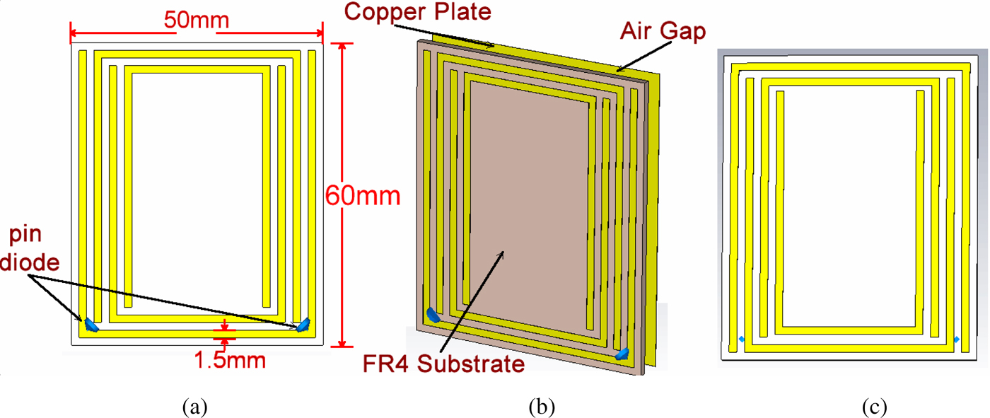
Fig. 1. Proposed structure for GSM band energy harvesting (a) front side, (b) profile view, (c) back view of the proposed structure.
The design details of the proposed structure can be seen in Figs 1(a)–1(c). The noted 1.5 mm value applies to both resonator thickness and resonator gap. These dimensions were chosen by evaluating a range of parametric studies to calculate the best available numerical and experimental results. The final design was produced using a CNC machine, and the experimental tests were conducted using a horn antenna connected to an 8 GHz vector network analyzer (VNA), as shown in Fig. 2(b). For the absorber and energy harvesting configuration tests, a single port with time gating in VNA was used (single-port Tx-Rx) to feed the horn antenna, with linearly polarized electromagnetic waves transmitted from the horn antenna with normal incidence to the manufactured test sample, which was compromised of 4 × 4 unit cells, as shown in Fig. 2(a). From the simulation and test results, the proposed structure's reflection coefficient value (S 11) is minimized at the GSM resonance frequencies of 900 MHz.

Fig. 2. (a) Unit-cell boundary application of simulation program, (b) manufactured sample of proposed structure.
Numerical simulation results were obtained using the CST Microwave Studio utilizing a finite integration technique. Absorption can be defined as a lack of transmission and reflection in the case of incidental radiation. Absorption can be calculated as A(ω) = 1 − R(ω) − T(ω) where A(ω), R(ω), and T(ω) define the absorption, reflection, and transmission values. When R(ω) = |S 11|2 and T(ω) = |S 21|2, A(ω) falls to the minimum value, and absorption rises to the maximum level at the given resonance frequency. No transmission will then be available due to the metal plate placed behind the air gap. In order to collect microwave energy, it is necessary to absorb energy in the MTM. For this reason, harvested energy rises the more nearly perfect absorption can be achieved. This energy can then be converted using a high-frequency Schottky diode. In this study, HSMS 2860 Schottky diodes were used in both the simulation and experimental sections. It is possible to reduce reflection to almost zero by choosing appropriate relative effective permittivity ε(ω) and permeability μ(ω) values to provide impedance that matches that of the air.
For absorbing and energy harvesting applications, unit-cell boundary conditions are applied along the − x and − yaxes, while an open additional space boundary is assigned along the +z direction and the wave is applied along the −z axis. The boundaries in CST are defined as unit cell, unit cell, open add space along the x, y, and z axes, respectively, as shown in Fig. 2(a). This type of selection provides a normal incidence wave that represents transverse electromagnetic wave propagation. Within both the simulation and tests, the angle of incidence's direction is –Z, and the polarization angle is 90°. For this application, the electric field vector is in the Y direction, while the magnetic field vector takes the X direction, as in Fig. 2(a). The frequency domain solver in CST Microwave Studio was used as the sole solver type throughout this paper, while experimental validation and tests were conducted on a manufactured sample of 4 × 4 unit cells, as shown in Fig. 2(b).
III. SIMULATIONS AND EXPERIMENTAL RESULTS
A model of the proposed structure, as shown in Fig. 2(b), was created using CNC machining, and experimental tests were conducted using a horn antenna connected to a 42.5 GHz VNA, as shown in Fig. 3. For testing, a single port with time gating in VNA was used (single-port Tx-Rx) to feed the horn antenna, and linearly polarized electromagnetic waves were transmitted from the horn antenna with normal incidence to the manufactured test sample, which was compromised of 4 × 4 unit cells. Initially, reflection coefficient measurement of the proposed structure was completed.

Fig. 3. Laboratory test picture using single-horn antennas, a 42.5 GHz Agilent vector network analyzer.
The simulated and measured absorptivity graph was plotted as shown in Fig. 4. The figure shows that the proposed design has resonances at 900 and 1020 MHz. As harvested energy is directly related to the confined electromagnetic wave within the absorber, it will increase at the maximum absorption points. The simulated and measured absorptivity values are compatible with each other and they both indicate that the proposed design can be used as an energy harvester for the GSM 900 band. Based on modern communication needs, cell towers operate continuously at frequencies of 900 and 1800 MHz, which is why the proposed structure is designed for these frequencies. The simulated resonance frequency and absorptivity were thus defined as 900 MHz and 98%, and the measured ones were 900 and 95%. This difference is likely to be caused by production and calibration errors in the test laboratory. A further resonance occurred at 1020 MHz; in that frequency, the simulated and measured values of the absorptivity were 99 and 96%, respectively. Other resonances following these points were also defined by means of measurement and simulation, and at these points, some frequency shifts can be seen.

Fig. 4. Simulated and measured absorptivity of the proposed structure under unit-cell boundary conditions between 500 and 2 GHz.
A second resonance occurred in the air gap between the copper plate and rear resonators, and this will be examined in the following sections. Although this resonance appears to be unnecessary for GSM 900 band work, it may be used in future work to harvest further electromagnetic energy.
In order to explain the absorption mechanism of the proposed structure, surface current distribution and electric energy densities were investigated at resonance frequencies of 900 and 1020 MHz, and the simulated results are plotted in Figs 5(a) and 5(b). It can be seen from the figures that the electric energy is concentrated at the left and middle side of the resonators. The electric field component of incident wave excites free electrons causing a surface current, and the surface charge oscillates along the external electric field; this field causes magnetic dipole moment, and it is this dipole moment that causes resonance absorption. Parallel and anti-parallel surface currents can be seen in both figures. While parallel currents induce electric fields, anti-parallel currents result in magnetic fields. These responses couple with E and H components of the incident electromagnetic wave and produce a strong localized electromagnetic field at the resonance frequency. Due to the larger absorption value at 1020 MHz, the surface current values in this instance are bigger than those seen at 900 MHz.

Fig. 5. Simulated surface current distribution: (a) surface current distribution at 900 MHz resonance, (b) simulated surface current distribution at 1.02 GHz.
In order to examine the material parameters between 0.5 and 2 GHz, Re(ε), Re(μ), and Re (n), which represent the permittivity, permeability, and refractive index of the proposed structure, are extracted by using scattering parameters. Figure 6 is plotted between 0.5 and 2 GHz in order to demonstrate the change in material parameters. Negative permittivity values are seen to cause a negative refractive index at 900 MHz.
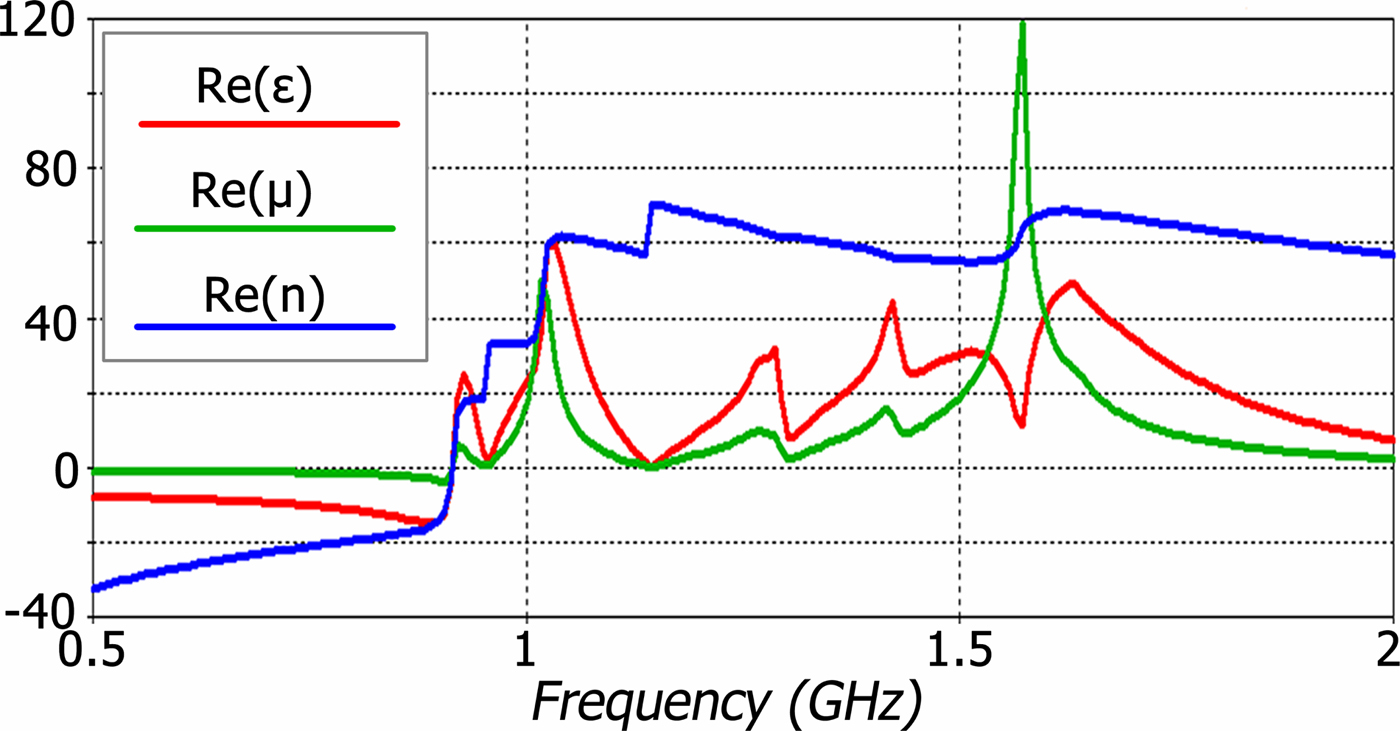
Fig. 6. Extracted material parameters of permittivity, permeability, and refractive index from 0.5 to 2 GHz for the proposed structure.
A) Effects of the air gap on the reflection coefficient
The proposed design offers a tuning function by means of changing the air gap distance between the copper plate and the rear resonators. As the distance between parallel plate capacitors is inversely proportional to their capacitance value, theoretically, as the distance increases, capacitance decreases and resonance frequency increases; this can be thought of as a tank circuit. Using this theory, a simulation of air gap distance was added to the observations to reflect the effects on the reflection coefficient. In order to support the simulation study, an experimental study was also performed. As it is easy to adjust the distance by using different amounts of substrates, 1.6, 3.2, and 4.8 mm air gap distance values were chosen as a sample of possible distances; the simulation and experimental study results of this are shown in Fig. 7. When air gap distance is adjusted to 1.6 mm, resonance frequencies occur at 1730 and 1050 MHz. If the distance is increased to 3.2 mm, the resonance frequencies shift to 1600, 1030, and 930 MHz. Finally, when the air gap distance becomes 4.8 mm, the resonance frequencies become 1020 and 900 MHz, as theoretically predicted. These values verify the capacitance and tank circuit approach to resonance frequency shifts in reflection coefficients. Absorptivity in these frequencies is higher than 90%, which increases the captured energy level available for energy harvesting applications. By using this property, the proposed structure can be utilized for energy harvesting at 900 and 1800 MHz. As shown in Fig. 7, the air gap can therefore be used for tuning resonance frequencies in energy harvesting applications in the ultra high-frequency (UHF) band.

Fig. 7. Absorptivity simulation and experimental study with three different air gap samples: (a) 1.6, (b) 3.2, and (c) 4.8 mm.
B) Effects of the Schottky diode on energy harvesting
In order to show the effects on the reflection coefficient of using the Schottky diodes (HSMS 2860), simulation and experimental studies were implemented. The sample was produced by using a CNC PCB machine, as shown in Fig. 8(a), and then tested. The simulated and experimental results are given in Fig. 8(b). Comparing this figure with the previous results, it is clear that the resonance frequency is shifted by about 10 MHz and the reflection coefficient level increases by about 10%. The simulation and experimental study results agree with each other except for a 15 MHz shift, which is due to production and calibration errors. As it is seen from the figures, the existence of Schottky diodes does not significantly affect the reflection coefficient for energy harvesting applications, and they must be used in order to convert incidental electromagnetic wave energy within the resonators.

Fig. 8. (a)Sample used for illustration of Schottky diode effects, (b) simulated and measured reflection coefficients in dB of the proposed structure when Schottky diodes are not used as a lumped network element.
An alternative to a Schottky diode, a resistor, can also be used to harvest energy by acting as a load resistor. In order to show the effects of resistor value on harvested energy, a set of simulations was prepared. Here, the resistor value was changed between 5 and 25 Ω, with a step of 5 Ω. The simulation results showed the RF to DC conversion performance, and this value is important to create efficient energy harvesting design, which will be calculated as in [Reference Almoneef and Ramahi13]
 $$\rho = \displaystyle{{P_{DC}} \over {P_{RF}}}.$$
P RF is defined as 1 W by the simulation program manufacturer, and the P DC values are extracted from the voltage and current values of the resistors used in this study. To facilitate numerical validation, resistors were placed between outside and inside resonators in place of Schottky diodes. The power harvesting efficiency graph for this case at 900 MHz is given in Fig. 9. As can be seen from the figure, the simulated power for different resistance values increases as the resistance value increases. Maximum power efficiency is numerically found to be 0.43 W between 15 to 25 Ω, and this decreases linearly between 5 and 25 Ω, with minimum power harvesting efficiency found as 0.41 W. In order to measure the voltage across the lumped elements without using a rectifier circuit, the Schottky diode is therefore used as a lumped network element.
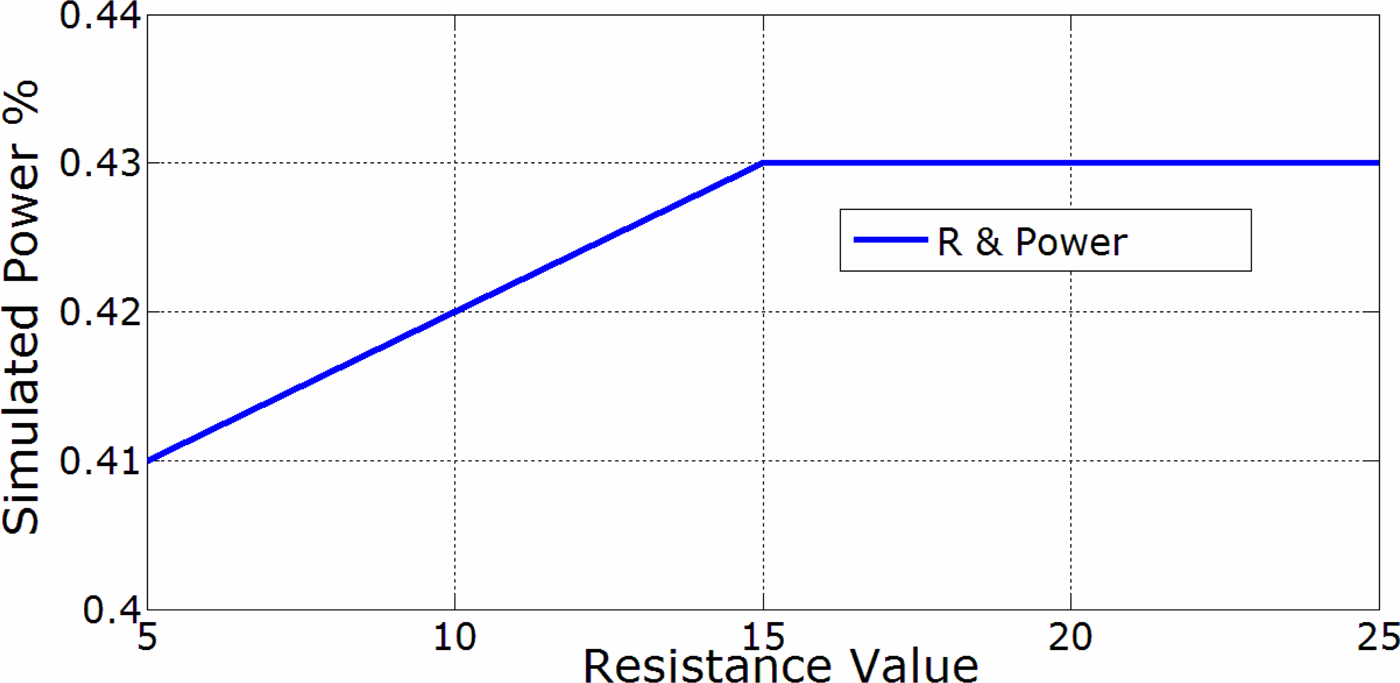
Fig. 9. RF to DC efficiency at different resistor values when used as a lumped network element.
C) Effects of orientation
In this section, the effects of geometry on the front and rear resonators are analyzed by means of simulation. When U-shaped elements are placed on the FR4 substrate, as shown in Fig. 10, the resonance points at 900 MHz remain the same but the resonance at 1020 MHz is removed. Any additional resonance points differ from the previous ones. Based on the results, the geometry of U-shaped elements geometry also appears to be appropriate for use at 1 and 1.5 GHz for energy harvesting.
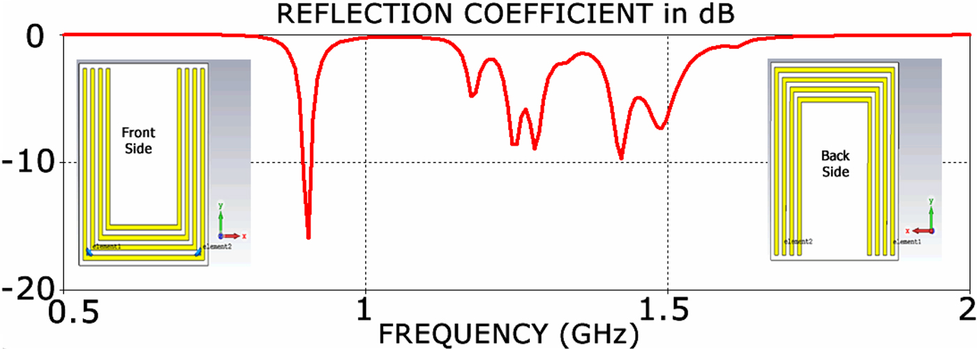
Fig. 10. Effects of the U-shaped elements’ geometry on absorptivity between 0.5 and 2 GHz.
D) Effects of angles of incidence and polarization
In this section, the angle of incidence and polarization angle under normal incidence have been simulated to show the proposed structure's angle insensitivity. The polarization angle (Φ) and angle of incidence (θ) are defined as “phi” and “theta” on the excitation port of the simulation program. Absorptivity for each of the Φ and θ angles is plotted by varying the “phi” and “theta” values on the port for the angles of 0, 20, 40, and 60°. Absorptivity is simulated under oblique incidence by changing the “theta” value. Then, after simulating and plotting absorptivity versus the θ angle of incidence, the polarization angle, Φ, is simulated by using normal incidence (θ = 0). The results are presented in Figs 11(a) and 11(b). As shown in the figures, absorptivity is not affected by either angle, which is an important requirement of absorber and energy harvesting applications.
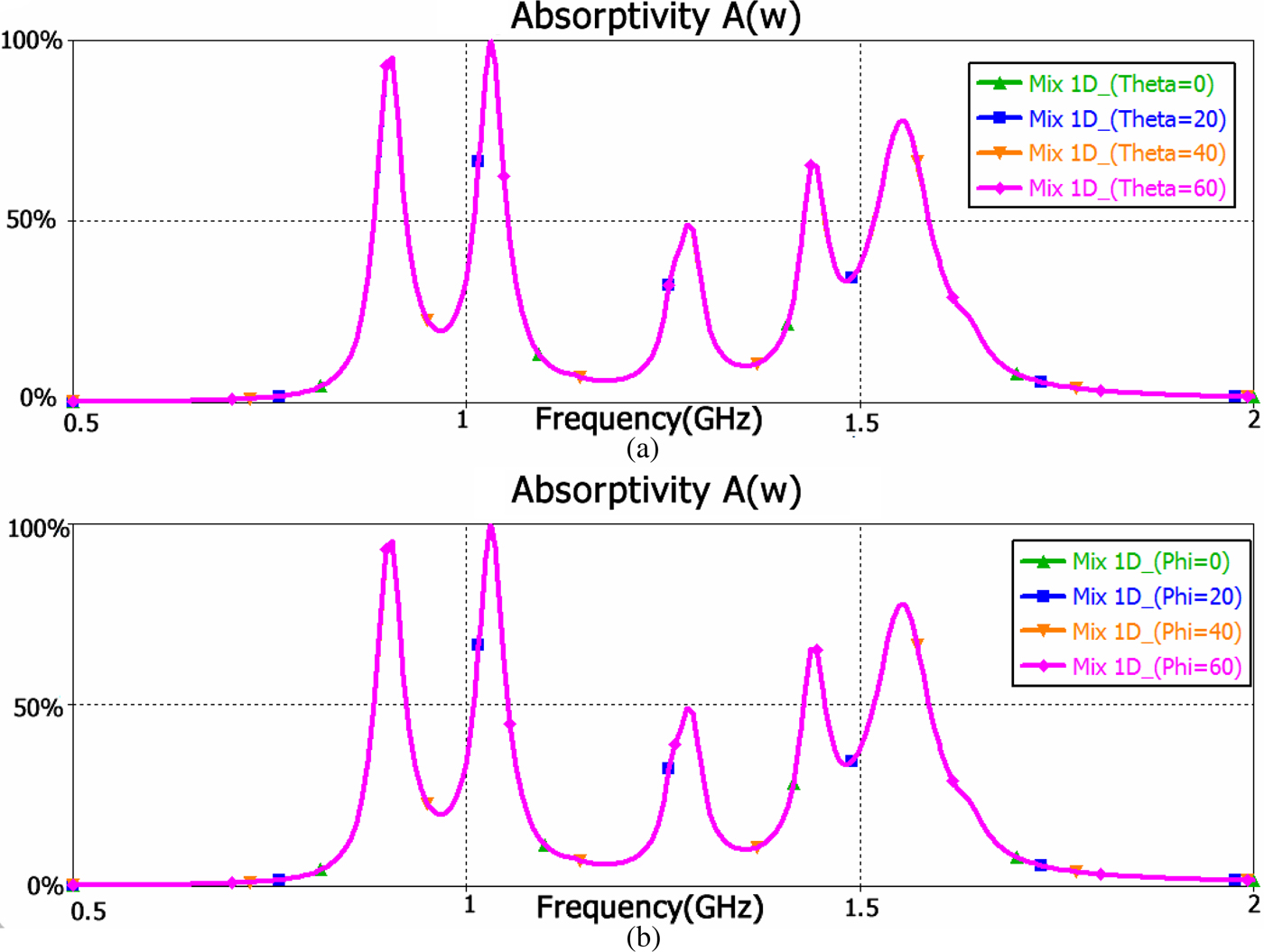
Fig. 11. Simulated absorptivity versus frequency for the proposed structure, (a) θ angle is set to different values between 0 and 60°; simulated absorptivity is presented. (b) The Φ polarization angle is set to different values between 0 and 60°; simulated absorptivity is presented.
In order to show the angular stability of the proposed structure, the angle of incidence (θ) was varied from 0 to 60° in steps of 20° and the absorptivity results are presented in Fig. 12. As seen in the figure, the proposed structure's absorptivity value is not affected by this angle. As electromagnetic waves can be excited by different sources, angle independency is an important parameter for energy harvesting applications. This independency is obtained in this instance by utilizing the unique structure of the U-shaped elements.

Fig. 12. Simulated absorptivity versus different polarization angles, Φ, (a) simulated absorptivity when θ is set to 0, (b) simulated absorptivity when θ is set to 20, (c) simulated absorptivity when θ is set to 60.
IV. ENERGY HARVESTING
A) Simulated energy harvesting
In order to investigate energy harvesting efficiency between 0.5 and 2 GHz, power across the Schottky diode was simulated using CST Microwave Studio; the energy harvesting simulation study results are given in Fig. 13. According to the figure, the absorbing efficiency is 0.5 W, which corresponds to 50% efficiency if the radiated power is assumed to be 1 W as set by the simulation program manufacturer. Simulated power becomes maximized at 1020 MHz, as expected. The simulated power at 900 MHz was defined as 0.48 W, which is sufficient when compared with previous energy harvesting study results [Reference Almoneef and Ramahi12–Reference Karaaslan, Ünal, Tetik, Delihacioğlu, Karadağ and Dincer15]. This simulation also verifies that harvested energy becomes maximized at the resonance points of the reflection coefficient between 0.5 and 2 GHz.
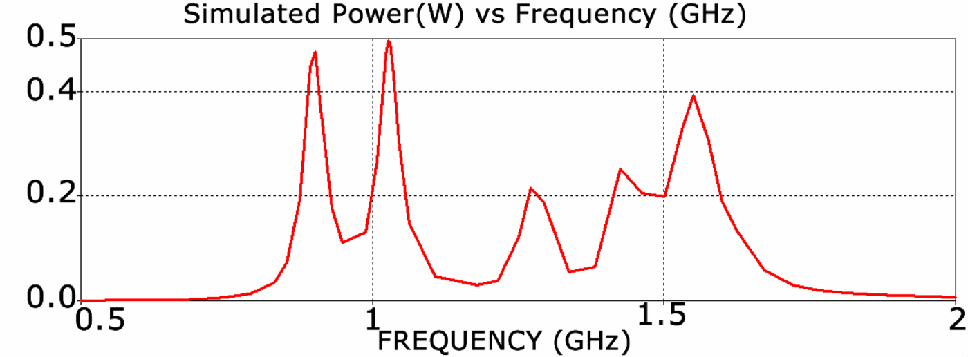
Fig. 13. Simulated power across the Schottky diode (HSMS 2860) between 0.5 and 2 GHz.
An impedance versus frequency plot of the structure is essential to ascertain the maximum power harvesting capabilities, and this is thus plotted in Fig. 14. As seen in the figure, the real and imaginary parts of the impedance change suddenly at the resonance points. The maximum value of the impedance is calculated at 1.6 GHz, with a value >1000 Ω.
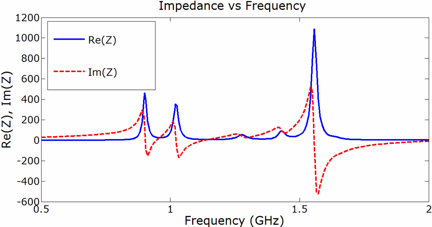
Fig. 14. Real and imaginary parts of the impedance plot between 0.5 and 2 GHz.
1) EXPERIMENTAL TESTING FOR ENERGY HARVESTING
In this section, two different measurements were implemented by using a Rohde & Schwartz FSH 8 hand-held spectrum analyzer and voltmeter measurements. These allowed measurement and investigation of the signal across the Schottky diode. In order to show the experimental study results, a sample structure, composed of a single cell, was produced and placed between two horn antennas, as shown in the Fig. 15(a). The horn antennas were connected to a Rohde & Schwartz 6 GHz network analyzer, and the HSMS2860 poles were connected to an 8 GHz spectrum analyzer using a SMA connector. The spectrum analyzer measurements are presented in Fig. 15(a). As the figure shows, a 40 dBm difference occurs at 900 MHz; however, at 1020 MHz, no resonance points are seen, while additional resonances can be seen at 1.5 and 2.5 GHz. As the laboratory in which these experiments took place does not have an anechoic chamber, disturbances do occur, and these can be seen from the spectrum analyzer screen.
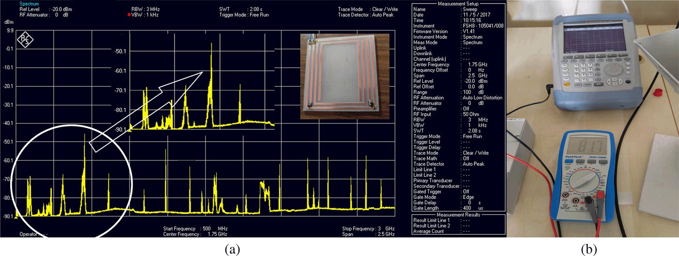
Fig. 15. (a) Sample for experimental study and spectrum analyzer view of the proposed structure between 0.5 and 3 GHz, (b) measured voltage across the HSMS 2860 Schottky diode.
V. CONCLUSION
MTM-based energy harvesting structures for UHF bands, particularly the GSM 900 and GSM 1800 bands, have been proposed. In order to demonstrate the absorption performance of these structures, reflection coefficients and absorptivity were validated using simulation and experimental methods. Surface current distribution was analyzed at 900 and 1020 MHz, along with polarization and angle of incidence independency. The results show that the proposed structure is independent of angle, which is an important feature for energy harvesting applications. In order to demonstrate energy harvesting efficiency, a simulation study was presented between 0.5 and 2 GHz. The effects of Schottky diodes and the air gap were verified using both simulation and experimental methods. Tests of the orientation of the U-shapes and air gap were simulated and the results are plotted for closer examination. In terms of energy harvesting performance measurements, the proposed structure was tested using a spectrum analyzer and voltmeter. Both simulation and experimental data show that the proposed structure can be used effectively for energy harvesting in UHF band applications. Although the measured output power of the proposed structure is low, it is sufficient to run low-energy consumption devices such as sensors and switches as in [Reference Devi, Ng, Kwong, Chakrabarty and Norashidah30, Reference Vullers, Schaijk, Visser, Penders and Hoof31]. As mentioned above, all papers should close with a conclusion section.
 Mehmet Bakır received his Ph.D. degree in Informatics at the Mustafa Kemal University in 2016. His main research interests are metamaterials, sensors, and energy harvesting devices. He has authored more than 20 research papers and conference proceedings.
 Muharrem Karaaslan received the Ph.D. degree in Physics Department from the University of Cukurova, Adana, Turkey, in 2009. He has authored more than 100 research papers and conference proceedings. His research interests are applications of metamaterials, analysis and synthesis of antennas, and waveguides.
 Olcay Altıntaş received the B.Sc. degree in Electrical and Electronics Engineering from the Cukurova University, in 2011 and received his M.Sc. degree at the Mustafa Kemal University in 2015. He is currently studying for Ph.D. in Electrical and Electronics Engineering from the Cukurova University, Turkey. His research interests are metamaterials, microwave and sensors, and antennas.
 Mehmet Bağmancı received his B.Sc. degree from the Mustafa Kemal University, Turkey in 2012. He is now working and receiving M.Sc. at the Iskenderun Technical University, Hatay, Turkey. He is the co-author of three scientific contributions published in international journals. His research interest includes metamaterials.
 Volkan Akdogan received a degree in Electronics and Communication Engineering from the Kocaeli University in 2009 and received his M.Sc. degree in Electrical and Electronic Engineering from the University of Nottingham in 2011. He received his Ph.D. degree in Renewable and Sustainable Energy Technology from the University of Nottingham in 2016. His main research interests are DC–DC converters for renewable and sustainable energy technology.
 Feyzullah Temurtaş received a degree in Electrical–Electronics Engineering from the Middle East Technical University in 1991 and received his M.Sc. and Ph.D. degrees in Electrical–Electronics Engineering in 1996 and 2000, respectively. Currently, he is the head of the Department of Electrical–Electronics Engineering at the Bozok University. He has over 100 publications in the field of Electronic Engineering.


