Introduction
The contemporary portable wireless communication devices need multi-functional antennas, which are adaptable to the changing system requirements. The reconfigurable antennas have received substantial consideration in recent years, due to their capability of changing frequency, polarization, or radiation pattern of the electromagnetic waves. The reconfigurability achieved can be single or it may be in the combination of two or more. As single antenna functions for multiple frequency bands, the frequency reconfigurability saves space and reduces the overall size of the device. The pattern reconfigurable antenna immensely augments the cellular system performance by steering the beam in the desired direction and improving the signal-to-noise ratio in the noisy environment. The reconfigurability can be realized through optical, electrical, or mechanical means, or by using special materials such as liquid crystals. However, the mechanical reconfigurable antenna systems have a complex and bulky configuration. Therefore, researchers are more interested in electrically reconfigurable antennas, as they have less complexity and are easy to fabricate. In the last decade, various reconfigurable antenna mechanisms have been reported by a number of researchers [Reference Haupt and Lanagan1–Reference Rani and Pandey19]. The frequency agile antennas using metamaterial elements were studied and developed in [Reference Cheribi, Ghanem and Kimouche2, Reference Hossain, Faruque, Islam and Ali3]. The antenna reported in [Reference Nasir, Afzal, Ijaz, Alimgeer, Shafique and Khan4] used epsilon negative transmission line for frequency reconfigurable characteristics, considering GSM and WLAN applications. In [Reference Huff and Bernhard5], radio frequency micro-electro-mechanical-system (RF MEMS) switches were integrated with a square spiral antenna for achieving pattern reconfigurability. The annular slot antenna in [Reference Gallo, Daviu, Bataller, Bozzetti, Pardo and Llacer6] utilized a dual-feed technique for pattern reconfigurability. The frequency and pattern agile antenna developed by embedding ground slot and two slits on the patch in [Reference Majid, Rahim, Hamid and Ismail7, Reference Selvam, Kanagasabai, Alsath, Velan, Kingsly, Subbaraj and Rao8]. The antennas with end-fire pattern reconfigurability using parasitic elements were investigated in [Reference Aboufoul, Parini, Chen and Alomainy9, Reference Sharma, Fideles and Kalikond10]. A mechanical and frequency reconfigurable antenna with two microstrip patches connected with one feed line was reported in [Reference Khan, Iftikhar, Capobianco, Shubair and Ijaz11]. The antenna based on reconfigurable matching network and the annular slot was realized in [Reference Nikolaou, Bairavasubramanian, Lugo, Carrasquillo, Thompson, Ponchak, Papapolymerou and Tentzeris12], for the pattern and frequency reconfigurability. The complementary split-ring resonator loaded pattern reconfigurable antennas with diverse radiation patterns were characterized and reported in [Reference Lu, Yang and Tan13, Reference Saurav, Sarkar and Srivastava14]. A dual-band dual-pattern patch antenna comprised of varactor diodes and four stubs with independent band tuning was reported [Reference Trong, Hall and Fumeaux15]. A dual-feed ultra-wideband (UWB) planar antenna with pattern and polarization diversity was presented [Reference Dong and Itoh16]. Further, the polarization-agile antennas with L-shaped [Reference Yoon, Baik, Lee, Pyo, Han and Kim17] and staircase ground slots [Reference Yang, Yang, Hong and Li18] were studied and developed. Recently, a dual-band coplanar waveguide (CPW)-fed antenna inspired by 90° rotated electric-inductive-capacitive (ELC) resonator was proposed [Reference Rani and Pandey19]. However, most of the reported reconfigurable antenna designs have complex geometry, relatively large size, limited operating bands, and less design flexibility.
This work presents a simple, compact, low-cost, parasitic ELC resonator-based reconfigurable antenna exhibiting frequency and pattern diversity. The proposed antenna is suitable for steering omni-directional radiation pattern into bi-directional and uni-directional end-fire radiation patterns for multiple frequencies. DC bias circuit is installed on parasitic elements to control the state of PIN diodes. The DC bias circuit is simple and does not involve vias, RF inductor coils, or DC blocking capacitors for its designing. Since the diodes are implemented on the ground plane, the DC bias lines are not required for connecting PIN diodes to the parasitic elements [Reference Yoon, Baik, Lee, Pyo, Han and Kim17, Reference Yang, Yang, Hong and Li18]. Compared to the above-mentioned antennas [Reference Haupt and Lanagan1–Reference Patel, Argyropoulos and Kosta22], the designed antennas do not need multiple feeding ports and complex geometry to achieve reconfigurability. Also, the proposed antenna does not require an extra matching network compared to the antennas in [Reference Huff and Bernhard5] and [Reference Nikolaou, Bairavasubramanian, Lugo, Carrasquillo, Thompson, Ponchak, Papapolymerou and Tentzeris12]. The paper is organized into four sections. The design process, specifications, and parametric study of the proposed reconfigurable antenna are presented in section “Antenna design”. The experimental and simulated results are discussed in section “Results and discussion” and section “Conclusion” presents a brief conclusion.
Antenna design
Figure 1 shows the geometry of the proposed reconfigurable antenna. The proposed CPW-fed antenna is comprised of a parasitic ELC resonator and closed ring resonator (CRR), both connected through a PIN diode. Four metal strips of different lengths are introduced on the two sides of the resonators; the two metal strips (which act as a parasitic element) on each side are connected by using PIN diodes (SMP1345-040LF Skyworks) as shown in Fig. 1(a). The overall size of the proposed antenna is 34 mm × 29 mm × 1.6 mm. A low-cost FR-4 substrate with a relative permittivity of 4.4, loss tangent 0.02, and thickness (h) 1.6 mm is used for fabricating the prototype antenna. The optimized dimensions of the proposed antenna are given in Table 1.
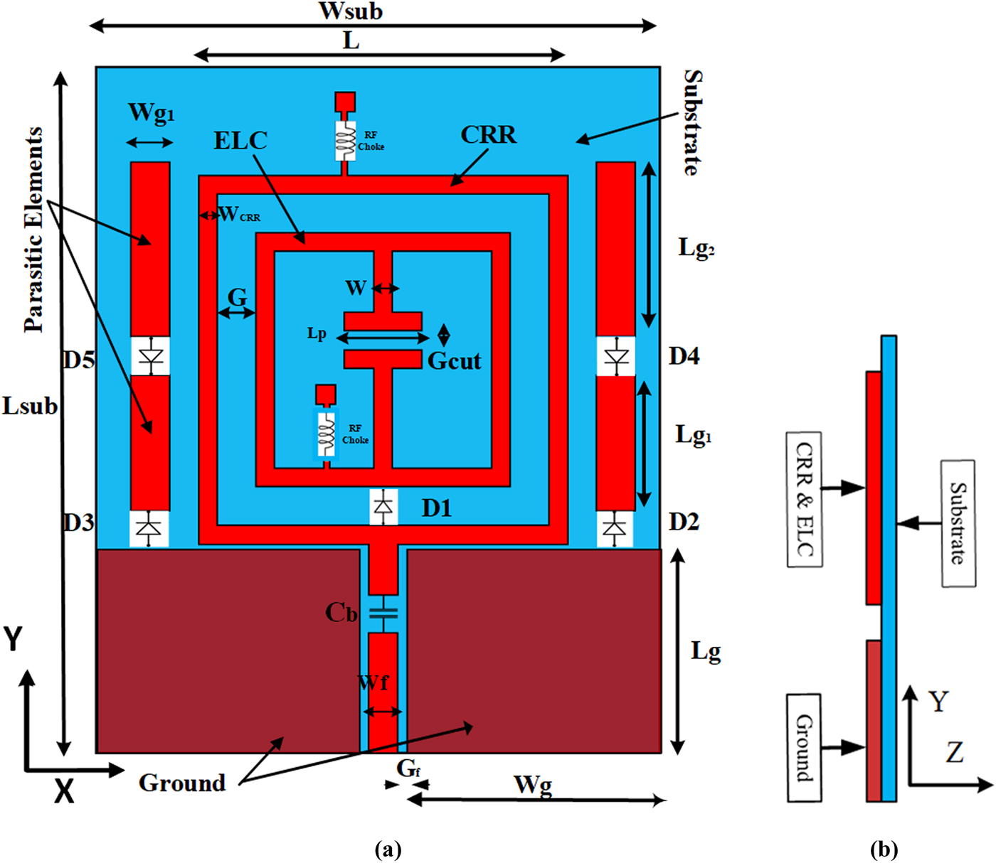
Fig. 1. Geometry of the proposed reconfigurable antenna: (a) top view, (b) side view.
Table 1. Dimensions of the proposed reconfigurable antenna
The design process of the proposed reconfigurable antenna is explained in two sub-sections as follows:
Design flow
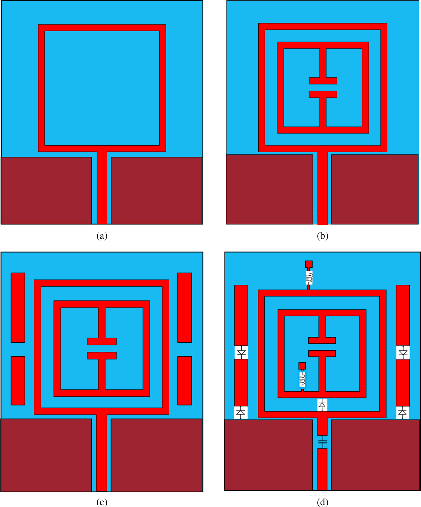
The antenna designing steps are presented in Fig. 2. Figure 3(a) signifies the simulated return loss characteristics of the antenna evolution steps. The antenna designing starts from a simple square loop resonator (Antenna 1) as shown in Fig. 2(a). The square loop antenna resonates for a single band. In the next step, the proposed Antenna 1 is loaded with a parasitic ELC resonator (Antenna 2) as illustrated in Fig. 2(b). Subsequently, Antenna 3 is proposed by introducing rectangular parasitic strips as shown in Fig. 2(c). The Antenna 2 shows dual-band resonance while Antenna 3 resonates for three bands. Here, the motivation was to design a pattern reconfigurable multiband antenna.

Fig. 2. Design flow of the proposed antenna: (a) Antenna 1, (b) Antenna 2, (c) Antenna 3, (d) Antenna 4.
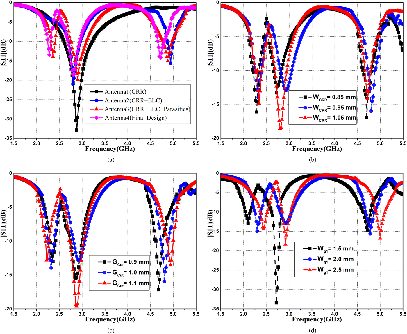
Fig. 3. (a) Simulated S 11 of antenna designing steps, (b) S 11 variation of Antenna 3 with CRR width (W CRR), (c) S 11 variation of Antenna 3 with ELC gap width (G cut), (d) S 11 variation of Antenna 3 with parasitic width (W g1).
Parametric analysis of the proposed antenna
The proposed antenna designing begins with a CRR loaded Antenna 1 (with a side length of 19 mm), resonating at 2.87 GHz. Antenna 2 is obtained by introducing a parasitic ELC resonator of side length 15.1 mm inside the CRR, with a self-resonance frequency of around 5 GHz. The ground plane of the antenna is optimized for dual-band operation. Antenna 2 resonates at two bands with center frequencies 2.8 and 4.9 GHz. The upper band at 4.9 GHz is due to the ELC resonator. Owing to the mutual coupling effect between the two resonators in Antenna 2, a small shift in the resonating frequencies is observed, as depicted in Fig. 3(b). Antenna 3 is realized by loading four rectangular parasitic elements at the two ends of Antenna 2. Antenna 3 resonates for three frequency bands centered around 2.35, 2.8, and 4.8 GHz. The middle resonating band (2.8 GHz) of the square CRR is affected by the variations in CRR width (W CRR). The CRR width is optimized for triple-band operation and its effects are demonstrated in Fig. 3(b). The upper resonating frequency (4.8 GHz) of Antenna 3 is affected by variations in the ELC resonator gap width (G cut) between the stubs. The G cut is optimized for triple-band operation as shown in Fig. 3(c). The lower resonating frequency (2.35 GHz) of Antenna 3 is affected by variations in parasitic element width (W g1). The value of W g1 is optimized for triple-band operation which is shown in Fig. 3(d). Further, the PIN diodes are embedded in Antenna 3 to obtain the final design. The layout of the proposed triple-band reconfigurable Antenna 4 is shown in Fig. 2(d). The ground plane is further optimized for impedance matching at three frequency bands centered around 2.28, 2.8, and 4.7 GHz.
Results and discussion
The antenna return loss is measured using Agilent PNA-L N5230A network analyzer and radiation patterns are measured inside an anechoic chamber. Five SMP1345-040LF PIN diodes from Skyworks are utilized for reconfiguring the proposed antenna. The diode offers a resistance of 1.5 Ω in series with an inductance of 0.45 nH in ON condition. While in OFF state it offers 0.45 nH inductance in series with a shunt capacitance of 0.2 pF and a resistance of 500 KΩ. A DC blocking capacitor of 20 pF and RF choke inductor of 22 nH are used to isolate DC bias and RF feed lines. The DC biasing lines are fabricated with smaller dimensions so they may have little impact on antenna radiation and impedance characteristics. In the proposed design, to minimize the effect of bias line on antenna performance, the bias lines are made orthogonal to the radiator. The fabricated DC bias lines have a width of 0.3 mm and a length of 2 mm. Figure 4 shows the photograph of a fabricated ELC resonator-based reconfigurable antenna.
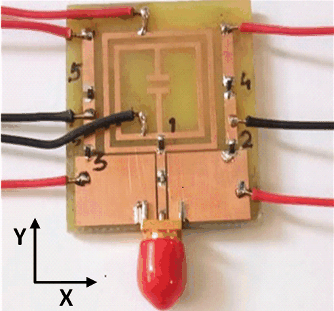
Fig. 4. Photograph of the fabricated reconfigurable antenna.
The operation mechanism of the proposed antenna is discussed here. The frequency diversity is achieved by exciting the CRR and ELC resonators separately and collectively, and by mutual coupling between the parasitic elements and two resonators. The PIN diodes implanted between the ground plane and four parasitic elements control the electrical length of the ground plane to accomplish pattern diversity. The ground plane and parasitic elements along with PIN diodes function as a reflector director or vice-versa, depending upon the state of implanted PIN diodes. The ground plane and parasitic elements jointly steer the primary omni-directional beam to bi-directional and uni-directional end-fire radiated beam at multiple frequency bands, depending upon the state of PIN diodes.
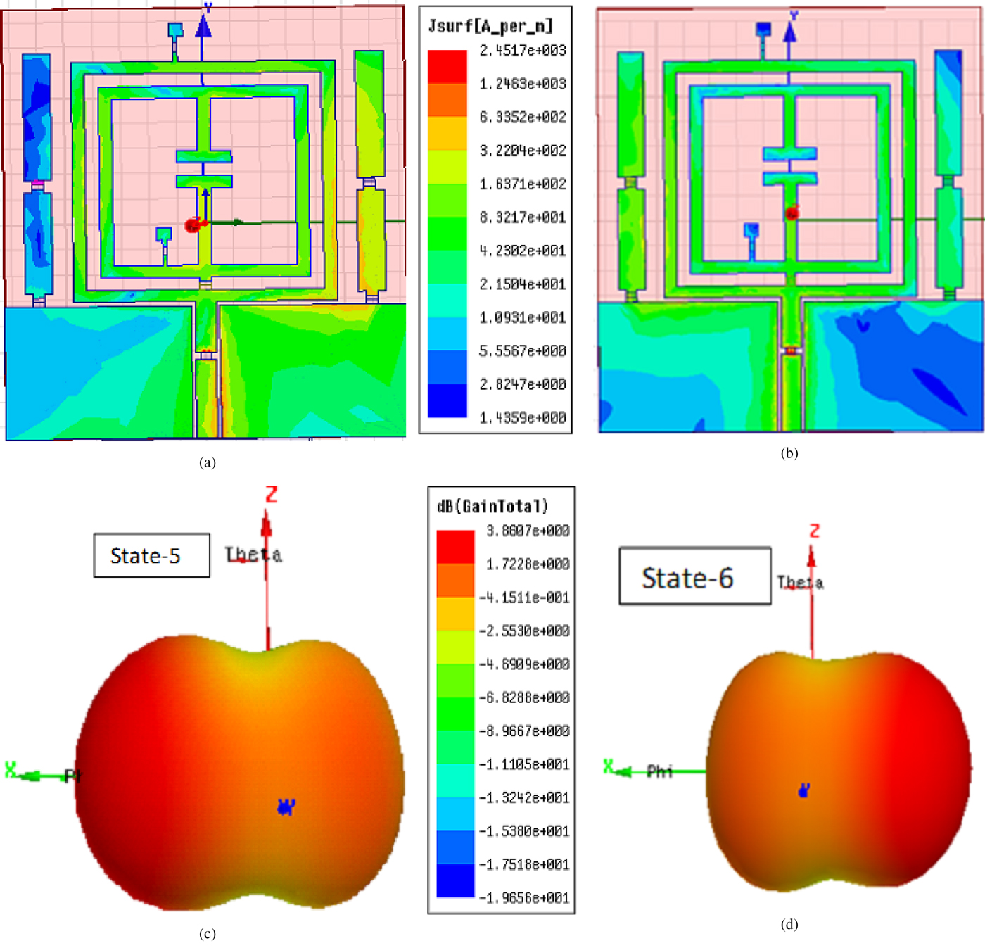
The surface current distribution is studied to interpret the end-fire beam reconfigurability. The simulated surface current distributions and 3D radiation patterns at 4.76 GHz, when the antenna is in state-5 and state-6, are illustrated in Fig. 5. It is noticed that when the diode D2 is ON, the parasitic element at the right end of the antenna is attached to the ground plane and work as a reflector, directing the main beam toward (+x) direction. Next, when the diode D3 is ON, the parasitic element at the left end is attached to the ground plane and works as a reflector, directing the main beam toward (−x) direction. This is due to the non-symmetrical distribution of surface current around the y-axis, on the resonator and on the ground plane. Here, the parasitic element and ground plane jointly work as a reflector. This results in an end-fire beam in the XZ- (H)-plane. When the parasitic elements are not connected to the ground plane, then they are not resonating [Reference Aboufoul, Parini, Chen and Alomainy9]. It is also clear from Fig. 6 that current distribution is symmetrical around the y-axis. The maximum current is concentrated along the outer surface of CRR and at the top edge of the ground plane, while very small current lies along the periphery of ELC. This type of surface current distribution results in an omni-directional beam in the XZ- (H)-plane.

Fig. 5. Simulated surface current distribution and 3D radiation pattern in end-fire mode: (a) surface current when diode D2 is ON, (b) surface current when diode D3 is ON, (c) 3D radiation pattern when diode D2 is ON (+x), (d) 3D radiation pattern when diode D3 is ON (−x).
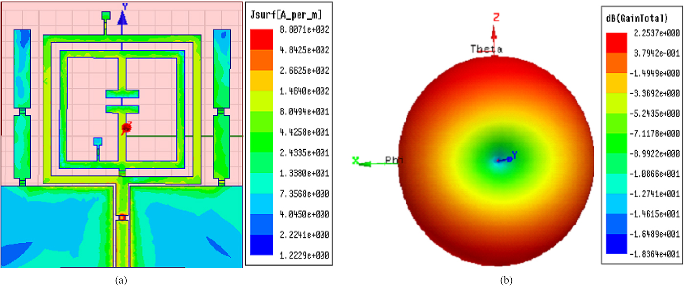
Fig. 6. Simulated surface current distribution and 3D radiation pattern in omni-directional mode: (a) surface current, (b) 3D radiation pattern.
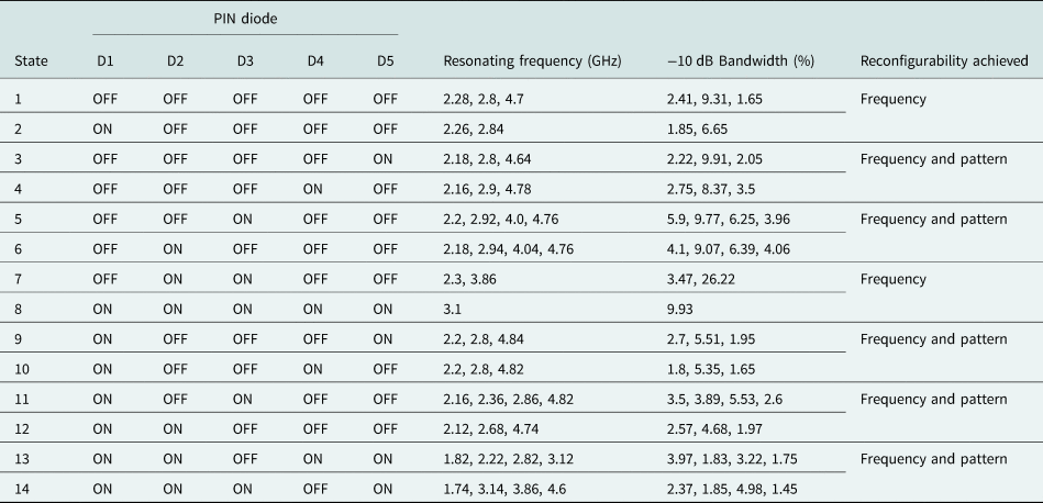
Each side of the parasitic element is configured with two PIN diodes. Initially, when all the diodes are in OFF state, the antenna operates in state-1, both ELC and CRR have no physical connection and parasitic elements are not connected to the ground plane. In this state, the antenna resonates for three bands (2.28, 2.8, and 4.7 GHz) and the radiation pattern is like a dipole antenna. Next, when only diode D1 is ON, the antenna operates in state-2 showing dual-band operation (2.26 and 2.84 GHz). Since the parasitic elements are not connected to the ground plane, the radiation pattern is the same as in state-1. Further, when diode D5 is ON and rest of the diodes are in OFF state, the antenna operates in state-3; in this case, the left-side parasitic elements work as a reflector for 4.64 GHz, while the right-side parasitic elements work as a director, this results in radiation in the (+x) direction and the pattern shows +90° shift at 4.64 GHz, while at 2.18 and 2.8 GHz, the pattern is omni-directional. Similarly, when the diode D4 is ON and rest of the diodes are in OFF state, the antenna operates in state-4; in this case, the right-side parasitic elements work as a reflector for 4.78 GHz, which results in shift in the (−x) direction, the pattern shows −90° shift at 4.78 GHz, while at 2.9 GHz, the pattern is omni-directional.
Furthermore, in state-5, when the diode D3 is ON and other diodes are in OFF state, the left-side parasitic element is connected to the ground plane and works as a reflector for three bands (2.2, 4, and 4.76 GHz). The main beam steers from omni-directional to end-fire (+90°). When the diode D2 is ON and other diodes are in OFF state, the antenna operates in state-6 and the right-side parasitic element is linked to the ground plane. At this point, the right-side ground plane and parasitic element jointly perform as the reflector. The main beam steers from omni-directional to end-fire (−90°) for three frequency bands (2.18, 4.04, and 4.76 GHz). When the diodes D2 and D3 are in ON condition, the antenna operates in state-7, and in this case, the parasitic elements on both sides get linked to the ground plane, which results in the split of the antenna fundamental frequency, 2.8 to 2.3 and 3.86 GHz with the omni-directional radiation pattern. Furthermore, when all the diodes are in ON state, the antenna operates in state-8, and in this case, all the parasitic elements are connected to the ground plane, with the fundamental frequency of 3.1 GHz and the omni-directional pattern.
When the diodes D1 and D5 are ON and other diodes are in OFF state, in this case, both the ELC and CRR are connected together and the antenna operates in state-9. In this state, the two left-side parasitic elements jointly work as a reflector resulting in an end-fire pattern (+90°) for 4.84 GHz, while at 2.2 and 2.8 GHz, the radiation patterns are omni-directional. When diodes D1 and D4 are ON, the antenna operates in state-10. In this state, the two right-side parasitic elements jointly work as a reflector for 4.82 GHz resulting in an end-fire pattern (−90°), while for 2.2 and 2.8 GHz, the main beam is omni-directional. Moreover, when the diodes D1 and D3 are ON, connecting ELC and CRR, the antenna operates in state-11. In this case, the left-side parasitic element connects to the ground plane, which operates as a reflector for three bands (2.16, 2.36, and 4.82 GHz), resulting in an end-fire beam (+90°). When the diodes D1 and D2 are ON, the antenna operates in state-12. In this case, the right-side parasitic element connects to the ground plane and works as a reflector for two bands (2.12 and 4.74 GHz), which provides end-fire beam (−90°).
When the diodes D1, D2, D4, and D5 are ON, the antenna operates in state-13. In this case, the two right-side parasitic elements connect to the ground plane and act as a reflector, which results in end fire (−90°) pattern for three bands (1.82, 2.22, and 3.12 GHz). When the diodes D1, D2, D3, and D5 are ON, the antenna operates in state-14, and the two left-side parasitic elements connect to the ground plane acting as a reflector, which results in end fire (−90°) pattern for two bands (1.74 and 3.86 GHz). Tables 2 and 3 show the detailed state-wise analysis of different diode combinations. Figure 7 shows the comparison between simulated and measured return loss characteristics for different states of PIN diode combinations (as mentioned in Table 2). Figure 8 depicts normalized simulated and measured radiation patterns in both E- (YZ) and H- (XZ)-planes for different diode combinations (as mentioned in Table 2). A comparative summary of the designed antenna with reported reconfigurable antenna designs is presented in Table 4.
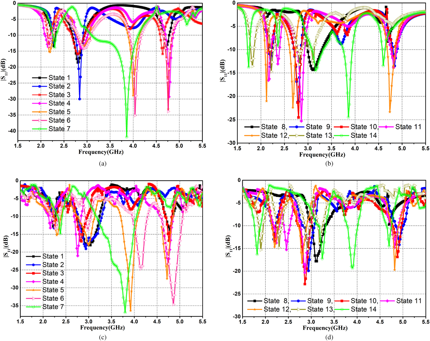
Fig. 7. Simulated and measured S 11 of the proposed antenna: (a) simulated S 11 for state-(1–7), (b) simulated S 11 for state-(7–14), (c) measured S 11 for state-(1–7), (d) measured S 11 for state-(7–14).
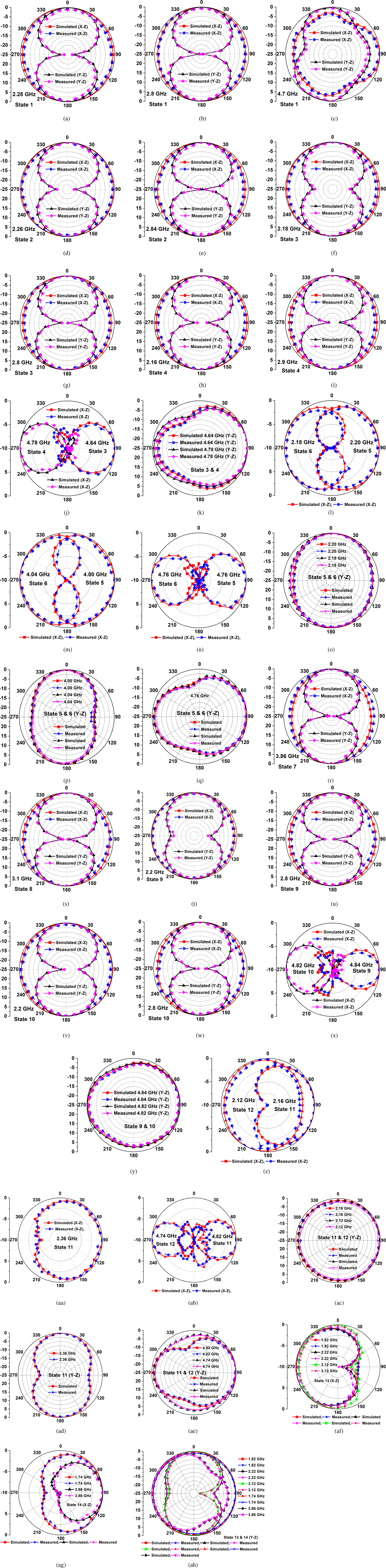
Fig. 8. Simulated and measured radiation patterns of the proposed antenna for state-1 to state-14 in E- (YZ) and H- (XZ)-planes.
Table 2. State table for the proposed reconfigurable antenna

Table 3. Simulated results for different states of the proposed reconfigurable antenna
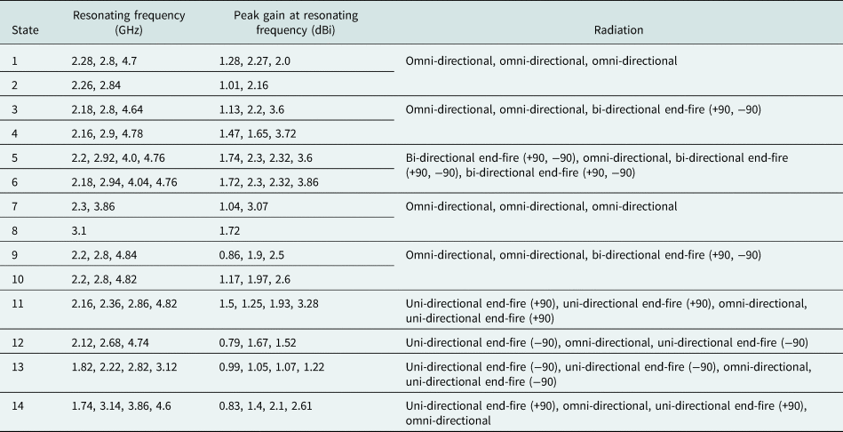
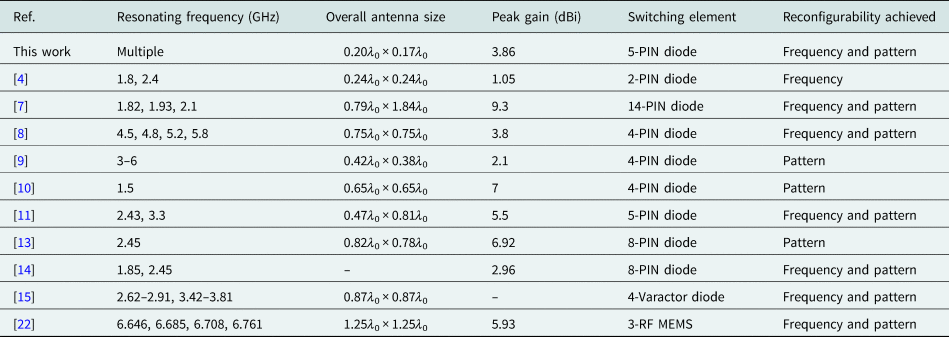
Table 4. Comparison between the proposed antenna and other reported reconfigurable antennas
Conclusion
In the present work, a compact, frequency, and pattern reconfigurable antenna is developed and tested. The proposed CPW-fed antenna is comprised of CRR and ELC resonators, four parasitic elements, and five switches. The proposed antenna shows frequency diversity by exciting resonances of CRR and ELC separately and collectively, through mutual coupling between the parasitic elements and resonators. The pattern diversity is realized by controlling the electrical lengths of the parasitic elements and ground plane. Depending upon the states of PIN diodes, the ground plane and parasitic elements together work as a reflector director or vice-versa and steer the primary omni-directional beam to bi-directional and uni-directional end-fire beams, at multiple frequency bands. The prototype of the proposed structure is fabricated and the experimental results show a close resemblance to the simulated results. The proposed antenna is simple to design, and has moderate gain and capability to alter its working frequency and radiation patterns. The antenna could be useful for back-to-back repeater systems.
 Ghanshyam Singh received his B.Tech. degree in Electronics and Communication Engineering from U.P. Technical University (presently known as Dr. A.P.J. Kalam Technical University) Lucknow, Uttar Pradesh, India, in 2004. He received his M.E. degree in Electronics and Communication Engineering from the National Institute of Technical Teachers Training and Research, Chandigarh, India, in 2013. He joined the Department of Electronics and Communication Engineering, Feroze Gandhi Institute of Engineering and Technology, Raebareli as a Lecturer in 2007. Prior to joining academics, Ghanshyam Singh had worked as an Electronics Engineer in the Railway Testing division of M/s Central Electronics Ltd. (A Govt. of India, DSIR Public Sector Enterprise). Currently, he is working towards his Ph.D. degree in Electronics Engineering from Dr. A.P.J. Kalam Technical University, Lucknow, India. His research interest includes patch antenna, artificial electromagnetic materials (LHMs/metamaterials), reconfigurable, and circularly polarized antenna for wireless communication. He has been credited to publish three research papers in peer-reviewed international journals and conferences.
 Binod Kumar Kanaujia is working as a Professor in the School of Computational and Integrative Sciences, Jawaharlal Nehru University, New Delhi since August 2016. Before joining Jawaharlal Nehru University, he had been in the Department of Electronics and Communication Engineering in the Ambedkar Institute of Advanced Communication Technologies and Research (formerly, Ambedkar Institute of Technology), Delhi as a Professor since February 2011 and an Associate Professor (2008–2011). Earlier, Dr. Kanaujia held the positions of a Lecturer (1996–2005), a Reader (2005–2008), and the Head of Department in the Department of Electronics and Communication Engineering, M.J.P. Rohilkhand University, Bareilly, India. Prior to his career in academics, Dr. Kanaujia had worked as an Executive Engineer in the R&D division of M/s UPTRON India Ltd. Dr. Kanaujia had completed his B.Tech. degree in Electronics Engineering from KNIT Sultanpur, India in 1994. He did his M.Tech. and Ph.D. degrees in 1998 and 2004, respectively, from the Department of Electronics Engineering, Indian Institute of Technology Banaras Hindu University, Varanasi, India. He has been awarded Junior Research Fellowship by UGC Delhi in the year 2001–2002 for his outstanding work in the electronics field. He has a keen research interest in the design and modeling of microstrip antenna, dielectric resonator antenna, left-handed metamaterial microstrip antenna, shorted microstrip antenna, ultra-wideband antennas, reconfigurable, and circular polarized antennas for wireless communication. He has been credited to publish more than 275 research papers with more than 1560 citations with h-index of 18 in several peer-reviewed journals and conferences. He had supervised 50 M.Tech. and 17 Ph.D. research scholars in the field of microwave engineering. He is a reviewer for several journals of international repute, i.e. IET Microwaves, Antennas & Propagation, IEEE Antennas and Wireless Propagation Letters, Wireless Personal Communications, Journal of Electromagnetic Wave and Application, Indian Journal of Radio and Space Physics, IETE Technical Review, International Journal of Electronics, International Journal of Engineering Science, IEEE Transactions on Antennas and Propagation, AEU-International Journal of Electronics and Communication, International Journal of Microwave and Wireless Technologies, etc. Dr. Kanaujia had successfully executed five research projects sponsored by several agencies of Government of India, i.e. DRDO, DST, AICTE, and ISRO. He is also a member of several academic and professional bodies, i.e. IEEE, Institution of Engineers (India), Indian Society for Technical Education, and The Institute of Electronics and Telecommunication Engineers of India.
 Vijay K. Pandey graduated in Electronics Engineering from The University of Poona in 1990. He obtained the M.E. degree in Control and Instrumentation with honors from Delhi University in 1997. He received his Ph.D. degree in Electronics Engineering from I.T. BHU Varanasi in 2006. At present he is working as a Professor in Electronics and Communication Engineering Department, Noida Institute of Engineering and Technology, Greater Noida, India. He received a grant of Rs.14.5 lakhs under MODROB scheme from AICTE, New Delhi for establishing Project and Research laboratory in the Department of Electronics and Communication. Professor Pandey has around 28 years of experience, teaching under graduate and post graduate classes. His research interest includes circularly polarized antennas, reconfigurable antennas, metamaterial-inspired antennas, and microwave components. He has published around 30 research papers in international/national journals and conferences of repute.
 Deepak Gangwar received his B.Tech. degree from Uttar Pradesh Technical University, Lucknow, India, in 2008, and the M.Tech. degree from Guru Gobind Singh Indraprastha University, Delhi, India in 2011. He received his Ph.D. degree in Electronics Engineering from the Indian Institute of Technology (ISM), Dhanbad, India. Currently, he is working as an Associate Professor in Bharati Vidyapeeth's College of Engineering, New Delhi, India. His research interest includes metamaterial-based antennas, ultra-wideband (UWB) antennas, metamaterial filters, frequency-selective surface, metasurface, and RCS reduction.
 Sachin Kumar received his B.Tech. degree in Electronics and Communication Engineering from Uttar Pradesh Technical University, Lucknow, India, in 2009. He received his M.Tech. and Ph.D. degrees in Electronics and Communication Engineering from Guru Gobind Singh Indraprastha University, Delhi, India, in 2011 and 2016, respectively. At present, he is working as a Researcher in the School of Electronics Engineering, Kyungpook National University, Daegu, South Korea. His research interests include circularly polarized microstrip antennas, reconfigurable antennas, UWB antennas, defected ground structure, and microwave components.