


Introduction
Wireless communications in backhaul networks are envisioned to take place at E-band (71–76 GHz and 81–86 GHz) and higher millimeter-wave frequencies due to the increasing demand for large bandwidths. In this context, power amplifiers are probably the most critical part. The continuous size downscaling of devices allows to operate at such high frequencies [Reference Scavennec, Sokolich and Baeyens1], but this entails also a reduction of the sustainable operating voltage and output power, as predicted by the Johnson limit [Reference Johnson2]. Power combining techniques are often needed to reach acceptable levels of transmitted power. Parallel current combining architectures represent the mainstream in this regard, but their moderate losses can impair the power amplifier performance. Moreover, their relatively large chip-area occupancy might be an issue. A viable alternative is the series voltage combining technique, known as stacked-transistor, where individual voltage swings of the single devices are summed up in phase keeping the current swing approximately unchanged in comparison with a single-device power cell. If n is the number of transistors connected in series, this results in an overall output power n times higher. Another potential benefit is that the optimum output load, defined as the ratio between the maximum voltage and current swings, also increases by the same factor, allowing a wider bandwidth and lower losses in the matching network. The stacked-transistor topology consists of a common-emitter (or common-source) stage followed by a series of n − 1 common-base (or common-gate) stages. It differs from the cascode because finite impedances are connected to the base of the common-base stages, making the base terminals experience a voltage swing to prevent base-collector breakdown. Collector-emitter breakdown is avoided by making the overall output voltage be equally divided among all the devices. This architecture has been successfully deployed at RF and microwave frequencies since its conception a couple of decades ago [Reference Shifrin, Ayasli and Katzin3–Reference Wu, Cheng, Li and Fu9], showing promising performances in terms of output power, gain, and efficiency. More recently, many research efforts have been exerted to extend the stacked-transistor concept at higher frequencies and into the millimeter-wave range [Reference Dabag, Hanafi, Golcuk, Agah, Buckwalter and Asbeck10–Reference Datta and Hashemi15]. An important condition to be satisfied for optimal performance is the interstage impedance matching between all the devices so as to limit internal reflections and power degradation. This aspect has been particularly emphasized in previous works and detailed analysis for calculating the common-base input impedance have been carried out. For operating frequencies much lower than the cut-off frequency f T, the transistors' reactive components have been neglected without significant loss of accuracy [Reference Pornpromlikit, Jeong, Presti, Scuderi and Asbeck5]. At high millimeter-wave frequencies, however, this simplification does not hold and layout-related parasitics must be characterized through electromagnetic (EM) simulations and taken into account [Reference Kim and Kwon13, Reference Datta and Hashemi15]. Several strategies have been proposed to accomplish the interstage matching condition, comprising series or parallel shunt inductive tuning and capacitive shunt-feedback tuning [Reference Dabag, Hanafi, Golcuk, Agah, Buckwalter and Asbeck10].
The stacked-transistor technique has been used mostly to overcome the limited breakdown voltage of silicon-based devices and GaAs HEMTs. Only a few works have been focused on applying this approach to InP Double Heterojunction Bipolar Transistors (DHBTs) [Reference Johansen, Yan, Dupuy, Nodjiadjim, Konczykowska and Riet16–Reference Squartecchia, Midili, Johansen, Dupuy, Nodjiadjim, Riet and Konczykowska18], and they were just limited to two-stacked topologies. InP DHBTs are proved to be well-suited for power amplifiers at high millimeter-wave frequencies thanks to high values of f T and f max, as well as moderately high breakdown voltage [Reference Hadziabdic, Krozer and Johansen19–Reference Urteaga, Griffith, Seo, Hacker and Rodwell21]. To the best of the authors' knowledge, this work represents an unprecedented attempt to extend the stacking technique to three and four InP DHBT transistors. The investigation follows a structured design flow starting from a small-signal analysis; it then includes large-signal models and finally accounts for the parasitic effects impairing the performance of the power cells. The latter step is particularly crucial and is carried out by means of extensive EM simulations [Reference Kassim and Malek22, Reference Thompson and Moore23]. Three- and four-stacked monolithic microwave integrated circuit (MMIC) matched power cells have been realized and measured for operation in the upper range of the E-band.
This paper is structured as follows: In the section ‘Circuit analysis and design’, the analysis and procedure for the design of DHBT stacked-transistors is described in detail, including layout optimization based on EM-circuit co-simulations. In the section ‘Implementations and experimental results’, the MMIC implementations of the matched power cells and their measured response are outlined. A four-way combined MMIC power amplifier based on three-stacked transistors is also reported together with measured results. Finally, in the section ‘Conclusion’, the results are summarized and discussed.
Circuit analysis and design
Figure 1 shows a conceptual schematic of a four-stacked transistor power cell (n = 4). It is composed of a common-emitter stage Q 1 followed by a series of three common-base stages Q 2–Q 4. For optimum output power and avoiding collector-emitter breakdown, all the devices must operate in phase under maximum voltage and current swing conditions. Base-collector breakdown is avoided by making all the base terminals swing with proper amplitude and phase, which is accomplished with the base capacitances C 2–C 4 providing finite impedances, in contrast with classical cascode implementation, where the base terminals are dynamically grounded. The base capacitances C k, together with the susceptances B k−1,k (k = 2,3,4), play also an important role for interstage impedance matching between the transistors. The parallel R 1–C 1 is essential to stabilize the circuit at low frequencies. In order to easily separate real and imaginary parts in the interstage matching design, admittances are considered instead of impedances as the elements to be tuned out are usually shunt parasitic capacitances. The bias network is omitted in the figure, but it should be noted that all transistors must operate with the same quiescent point, and since they are dc-coupled, a relatively high bias voltage could be required. In this section, we outline the theoretical relationships and the design procedure for properly dimensioning the circuit parameters for optimum operation. First, a calculation based on an approximated small-signal equivalent circuit is given. A more practical approach based on the large signal-model is described afterward and the real design with layout considerations will be finally presented.

Fig. 1. Conceptual circuit schematic of a four-stacked transistor power cell.
Small-signal analysis
The small-signal analysis of the stacked architecture is essential to understand the design principles. Like previous works on this subject, it can be conducted by considering the kth common-base stage for assessing its emitter input admittance Y in,k, which must be equal to the optimum load Y opt,k−1 of the preceding partial stack [Reference Wu, Cheng, Li and Fu9, Reference Kim and Kwon13, Reference Yan and Johansen17]. In doing so, we refer to Fig. 2, where a test voltage source v x is applied to the emitter terminal and the resulting current i x is evaluated. The interstage susceptance B k−1,k has been omitted in the figure as it can be considered separately as a mean to resonate the imaginary part of Y opt,k−1, so at the beginning, only the real part  $\Re [Y_{{in},k}]$ is of concern. The illustrated small-signal equivalent circuit corresponds to a single-finger InP DHBT biased at V ce = 2 V and I c = 15 mA, whose parameters have been extracted from measured S-parameters following the procedure described in [Reference Johansen, Leblanc, Poulain and Delmouly24]. Some simplifying assumptions are made: we neglected in this representation the distributed nature of the base resistance and of the base-collector capacitance, so we assumed R b = R bx + R bi and C μ = C bcx + C bci, where R bx and R bi are the extrinsic and intrinsic base resistances, respectively, and C bcx and C bci are the extrinsic and intrinsic base-collector parasitic capacitances, respectively. We assumed also that the emitter resistance R E and the collector resistance R C are small enough to be neglected. It should be noted that in this analysis, differently from some previous works, the feedback effects introduced by C μ and C ceo are carefully taken into account. At millimeter-wave frequencies, in fact, these represent an important contribution to the calculation of Y in,k, which strongly depends on the load admittance Y L,k. The relationship between the collector voltage v c and the emitter voltage v x, corresponding to the required voltage gain for in-phase voltage addition of the kth common-base stage is explicitly shown in the figure. In mathematical form, the following three conditions must be met simultaneously:
 $$\left\{ \matrix{\Re [Y_{in,k}] = \Re [Y_{opt,k - 1}] \hfill \qquad\qquad\qquad\qquad\qquad (1{\rm a})\cr \Re \left[ {\displaystyle{{v_c} \over {v_x}}} \right] = \displaystyle{k \over {k - 1}},\quad \quad (k = 2, \ldots ,n), \hfill \cr \Im \left[ {\displaystyle{{v_c} \over {v_x}}} \right] = 0,\qquad\qquad\qquad\qquad\qquad\qquad\qquad\qquad(1{\rm c}) \hfill} \right.{\hskip-17pt}(1{\rm b})$$
where the gain v c/v x has been found to have the following expression (see Appendix):
 $$\displaystyle{{v_c} \over {v_x}} = \displaystyle{{\left[ {\left( {sC_\mu + sC_{ceo}} \right)Z_b + \left( {g_m + sC_{ceo}} \right)\left( {1 + sC_\mu Z_b} \right)Z_\pi } \right]} \over \matrix{\left( {Y_{L,k} + sC_{ceo}} \right)\left( {Z_b + Z_\pi + sC_\mu Z_bZ_\pi } \right) \hfill \cr + sC_\mu \left( {Z_b + Z_\pi + g_mZ_bZ_\pi } \right) \hfill} },$$
with Z b = R b + 1/(sC k),  $Z_\pi =R_\pi /(1 + sC_{\pi }R_{\pi })$, and s = jω. Imposing the conditions (1b) and (1c) to (2), the admittance seen into the emitter can be calculated as:
 $$ Y_{{in},k}={\displaystyle{sC_{\mu}Z_\pi({k}/({k-1})) + 1} \over {Z_{b} + Z_\pi + sC_{\mu}Z_{b}Z_\pi}} + {\displaystyle{k} \over {k-1}} Y_{L,k}.$$
Fig. 2. InP DHBT small-signal equivalent circuit of the kth common-base stage for calculation of the input admittance Y in,k. Extracted parameters for a single-finger device with emitter area of 10 × 0.7 mum2 are: R b = 21.1 Ω, R π = 110 Ω, C π = 129.1 fF, C μ = 10.7 fF, C ceo = 4.9 fF, and g m = 403 mS.
At a given frequency and for a given transistor model, it can be seen that (1) is a system of three equations in the three unknowns C k,  $G_{L,k}=\Re [Y_{L,k}]$, and
 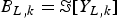 $B_{L,k}=\Im [Y_{L,k}]$, which can be solved numerically and verified with a circuit simulator. The calculated values of the unknown parameters are reported in Figs 3 and 4 as functions of the stack number k at different frequencies for a single-finger InP DHBT with an emitter area of 10 × 0.7 μm2. It can be observed that both the base capacitance C k and the load admittance Y L,k decrease as the stack number k and frequency increase.

Fig. 3. Theoretical values of the base capacitance Ck as a function of the stack number k for the kth common-base stage operating at different frequencies.

Fig. 4. Theoretical values of the load admittance YL,k as a function of the stack number k for the kth common-base stage operating at different frequencies.
The value of the interstage shunt susceptance B k−1,k is calculated for conjugate matching:
 $$ B_{k-1,k}=-\Im\left[Y_{opt,k-1}\right], $$
which is often implemented by means of an inductor L k−1,k tuning out the output parasitic capacitance of the (k − 1)th transistor. The latter condition ensures that the same current flows through all the devices.
Large-signal analysis
The above small-signal analysis is essential to get a useful understanding of the stacked-transistor concept and it is used to make a first estimation of the circuit parameters. However, it represents an idealization as real power amplifiers work in the large signal regime, near or well into saturation. Moreover, additional parasitics might be present, especially in multifinger devices, which are usually preferred to get higher power performances. A follow-up simulation using harmonic balance and large-signal transistor models is necessary in order to capture nonlinearities and additional parasitic effects. Besides interstage matching and in-phase voltage addition, power performances must be evaluated to determine the effectiveness of an additional stage along the stacked architecture. A structured design-flow for dimensioning all the parameters can be synthesized in a few essential points as illustrated in the flow-chart of Fig. 5. The initial step is the evaluation of the common-emitter power gain performances and optimum load Y opt,1 by means of a load-pull simulation performed on the large-signal model of the selected transistor. At millimeter-waves, in order to achieve acceptable gain and good linearity, Class A bias condition is selected. In this work, four-finger InP DHBT transistors featuring a breakdown voltage BV CEO ≈ 5 V and a maximum oscillation frequency f max > 350 GHz have been considered. A modified UCSD HBT model extracted from previous measurements is used in simulations with a bias point V ce = 2.4 V and I c = 60 mA [Reference Johansen, Midili, Squartecchia, Zhurbenko, Nodjiadjim, Dupuy, Riet and Konczykowska25]. The 86-GHz optimum load Z opt,1 = 1/Y opt,1 and the resulting load cycle for such a transistor in common-emitter configuration is shown in Fig. 6(a). A first estimation of the circuit parameters of the following common-base stage is then carried out by solving (1) and (4) in the small-signal analysis with k = 2. The found value Y L,2 can then be checked in large-signal regime by means of a load-pull simulation performed on the resulting two-stacked structure. All the parameters are then optimized so as to obtain maximum voltage and current swings for both devices, as shown in Fig. 6(b). In this way Y opt,2 is obtained and eventually used as the starting point in the design of the following third stage. This procedure can be iterated for the subsequent stages as long as positive incremental power gain is achieved. There will be a value of k for which P out,k ≤ P out,k−1. In this case n = k − 1 is the maximum number of transistors that can be stacked effectively. In Fig. 6, the optimized load cycles of the common-emitter, two-stacked, three-stacked, and four-stacked transistors operating at the 1-dB compression point at 86 GHz are shown. The power performance improvement of each stage is reported together with the corresponding increase of the load impedance level (or reduction of the load admittance) as predicted in the small-signal analysis. The values of the circuit elements of the optimized four-stacked transistor are reported in Table 1. In Fig. 7, the corresponding in-phase voltage waveforms taken at each collector node are reported. The improvements in terms of maximum available gain (MAG) are shown in Fig. 8, where a slight bandwidth reduction can be observed along the stacked architecture as a consequence of the inherently narrow-band reactive tuning of the design approach.

Fig. 5. Structured design flow for the design of an n-stacked transistor power cell.

Fig. 6. Optimized load cycles for common-emitter (a), two-stacked (b), three-stacked, (c) and four-stacked (d) 4 × 10 × 0.7 μm2 InP DHBTs transistors at 86 GHz. The input power is kept at Pin = 10 dBm in all cases.

Fig. 7. Collector voltage waveforms of the four-stacked transistor at 86 GHz after load cycle optimization.

Fig. 8. Maximum available gain of the optimized common-emitter, two-, three-, and four-stacked transistors.
Table 1. Circuit parameters for an optimized four-stacked transistor.

Layout
The InP technology used in this work comprises three TiPdAu metal layers (met1–met3) separated by polyimide for the realization of interconnections and transmission lines. A NiCr layer featuring 40 Ω/square is used for the realization of resistors and a thin Si3N4 layer serves for the realization of high-Q metal-insulator-metal capacitors with 0.49 fF/μm2. In Fig. 9, the schematic and layout views of the common-emitter, two-, three-, and four-stacked transistors are shown together with the respective optimized load cycles taken across each device after EM-circuit co-simulations and optimization carried out on ADS Momentum. The EM-circuit co-simulation approach ensures that all parasitics related to the particular layout and technology are accurately taken into account [Reference Kassim and Malek22, Reference Thompson and Moore23]. Resistive feedback networks are used as self-bias and for stabilization [Reference Green, Tozer and David26]. The EM-simulation approach ensures that all the parasitic effects are inherently taken into account during the optimization process.
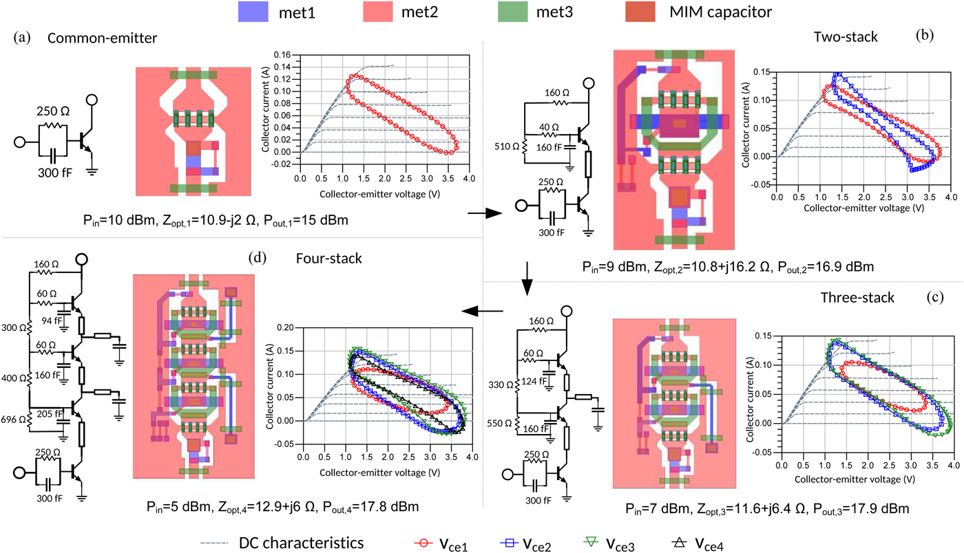
Fig. 9. Power cells layout of the common-emitter (a), two-stacked (b), three-stacked, (c) and four-stacked transistors (d) and corresponding simulated load cycles after EM-circuit co-simulation and optimization at 86 GHz.
As can be seen in Fig. 9(a), the optimum load of the common-emitter power cell has a small reactive component so a shunt interstage inductor was not necessary in the design of the two-stacked transistor. For the three- and four-stacked transistors, the shunt inductors L 2,3 and L 3,4 for interstage matching are realized by means of dynamically shorted coplanar waveguide (CPW) lines. Given the size constraints, the dc-blocking capacitors are of limited value and the equivalent LC series cause a resonance effect around 50 GHz. Another extremely important circuit component in the circuit layout is the finite-length emitter-collector interconnection between adjacent devices. This circuit element, in fact, represents the major limitation for efficient operation as it introduces significant phase misalignment between the collector voltages, as shown in the resulting waveforms of Fig. 10. However, technology-related design rules impose a lower limit on its length and some performance degradation seems unavoidable. In Fig. 9, the key performance metrics for the four designed power cells are reported. It can be seen that the gain improves considerably with the number of stacked transistors, while power performances are characterized by an earlier compression. For instance, the gain improvement of the three-stacked transistor over the two-stacked one is approximately 3 dB, while the output power at the 1-dB compression point is only one dB higher. The three- and four-stacked transistors exhibit comparable output power levels, but compression occurs at lower input power for the latter and, because of the higher bias voltage, it results also in a power added efficiency (PAE) degradation. Thus, it seems that the three-stacked transistor represents the best compromise in terms of gain and power performances.
Fig. 10. Collector voltage waveforms at 86 GHz of the four-stacked transistor taking into account layout parasitics.
Another layout-related effect can be noticed on the values of the optimum load impedances, whose values, differently from the schematic implementation, do not increase substantially with the number of stacked transistors. Some attention has to be drawn also to the effects of layout parasitics on the MAG. Fig. 11 shows the MAG comparison between pure schematic and layout designs. While the degradation for the common-emitter and the two-stacked transistors is due to extra parasitics of the layout implementations, the resonating effect of the shunt interstage CPW lines in the layout of the three- and four-stacked transistors makes their MAG decay considerably about 50 GHz. On the other hand, the series interconnects between the devices could be responsible for a small increase of the MAG at higher frequencies, an effect that can be somehow ascribed to an inductive peaking effect.
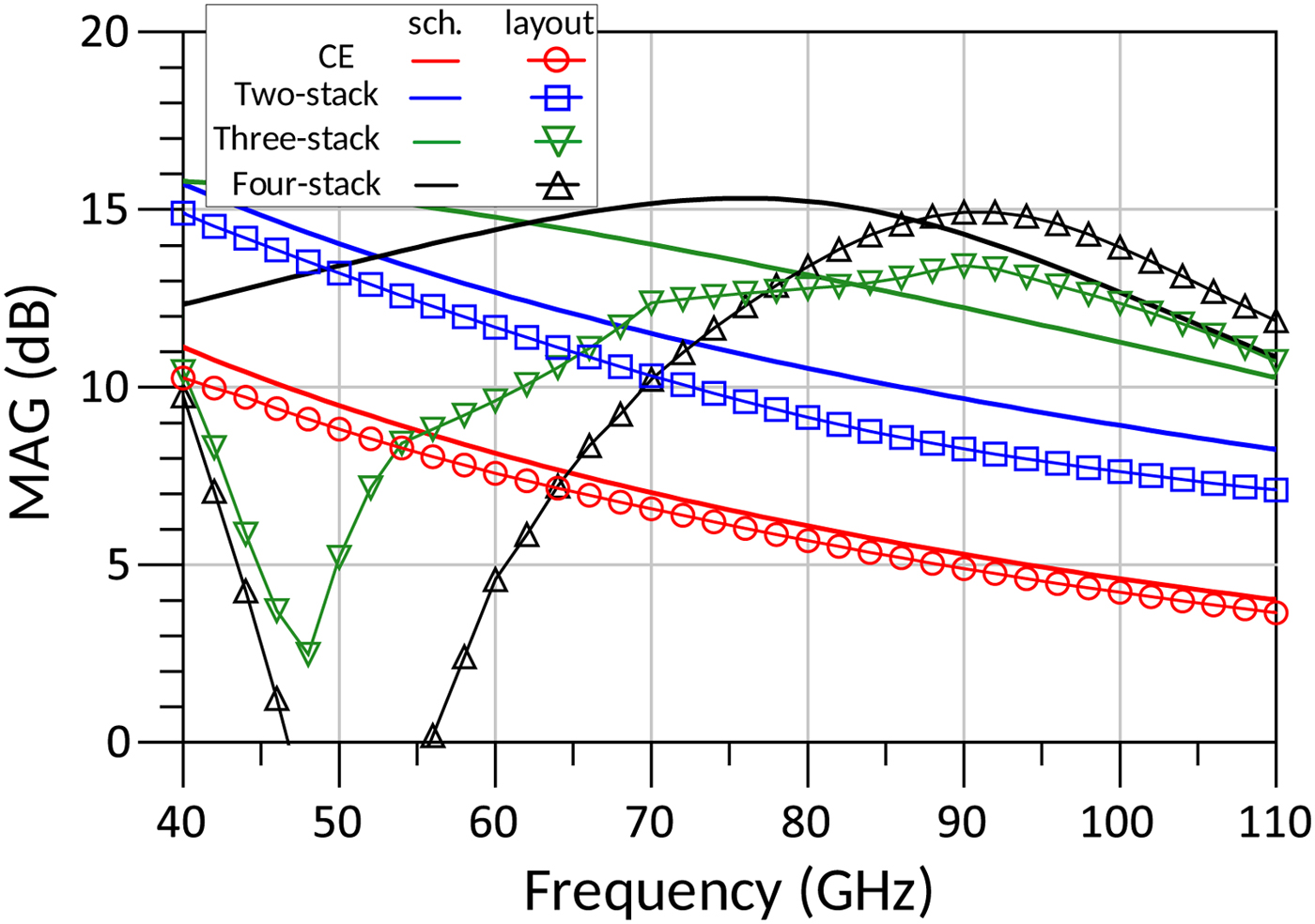
Fig. 11. MAG comparison between pure schematic design and taking into account layout parasitics for the four power cells.
Implementations and experimental results
The design principles described above have been verified experimentally for the three- and four-stacked transistors. The relative matched power cells have been implemented and tested in small- and large-signal operations. The matching networks have been designed using the in-house developed design-kit comprising all passive structures, including 50-Ω CPW transmission lines. Once again, all these structures have been previously characterized through extensive EM simulations. A four-way combined power amplifier employing three-stacked transistors has been realized as well, where a corporate power combiner is used. S-parameters measurements have been carried out on the wafer using RF GSG probe tips and the VNA MS4647 by Anritsu. For large-signal measurements, a custom-made test setup has been implemented, whose conceptual representation is shown in Fig. 12(a): a low-frequency sinusoidal signal is generated by the frequency synthesizer 68169B by Anritsu; the required E-band signal is then obtained by means of the frequency multiplier (×6) RPG AFM6 capable of a maximum output power of 7 dBm. A 0–50 dB variable attenuator and the 70–90 GHz medium power amplifier RPG 7090 are used together to vary the input power fed into the device under test. The output power level is measured with the power sensor W8486A and the power meter N1914A by Agilent. A shortcoming with this setup is that the maximum available power at the input probe tip is limited and its frequency dependence over the E-band range is reported in Fig. 12(b). This did not represent an issue in measuring simple power cells, but revealed as a significant restriction for multiple power-combined circuits, which could not be operated in saturation.

Fig. 12. Conceptual representation of the large-signal measurement setup (a) and calibrated maximum available input power at different frequencies (b).
Three-stacked transistor power cell
Figures 13(a) and 13(b) show the schematic and chip microphotograph, respectively, of the matched three-stacked transistor power cell. The bias voltages V cc and V bb are 6 and 1.7 V, respectively, resulting in a total current of 65 mA, including the current flowing in the resistive feedback network. The bypass capacitors C 1 provide dynamic shorts at the operating frequencies, while the series R 2–C 2 helps to attenuate eventual low-frequency oscillations. The MMIC size is 1.2 × 1.5 mm2. Measured and simulated S-parameters are reported in Fig. 14, where a good agreement can be observed, except for a frequency downshift of approximately 5 GHz most likely due to the input matching network, where bended CPW structures are used in order to comply with the chip-size requirements. The peak |S 21 | is 8.6 dB and occurs at 80 GHz. A 15-GHz 3-dB bandwidth is obtained in the range 70–85 GHz and the input return loss is better than 10 dB from 77 to 84 GHz. Simulated and measured large-signal performances at 81 GHz are reported in Fig. 15. It can be seen that the output power at the 1-dB compression point is approximately P out,1dB ≈ 12.5 dBm, with the corresponding input power P in,1dB ≈ 5 dBm. The saturated output power is P sat ≈ 15 dBm and the peak power-added efficiency resulted in PAE ≈ 5.2%. An excellent agreement between measurements and simulations is obtained at low power levels, somehow confirming S-parameter measurements. However, as the input power increases, the measured response seems to exhibit a slightly earlier compression. This can be due to a small difference in the output matching condition caused by the frequency downshift and to the accuracy of the large-signal modeling of the devices.

Fig. 13. Schematic (a) and chip microphotograph, (b) of the matched three-stacked transistor power cell. The chip size is 1.2 × 1.5 mm2.

Fig. 14. Simulated and measured S-parameters of the matched three-stacked transistor power cell.

Fig. 15. Simulated and measured power sweep of the matched three-stacked transistor power cell at 81 GHz.
Four-stacked transistor power cell
For the realization of the four-stacked transistor matched power cell (Fig 16), the requirements on the chip-size were less stringent and a straight matching network could be realized. The MMIC size, in this case, is 2.4 × 1.5 mm2. The only difference in the bias setting with respect to the three-stacked power cell is a higher V cc, which in this case is 8 V. The measured and simulated S-parameters are reported in Fig. 17, where a peak |S 21| of 11.4 dB at 83 GHz is observed. A 12-GHz 3-dB bandwidth is obtained from 74 to 86 GHz and the input return loss is better than 10 dB from 78 to 88 GHz. The power sweep response at 81 GHz is shown in Fig. 18, where the output power at the 1-dB compression point is observed around P out,1dB ≈ 12.5 dBm with an input power P in,1dB ≈ 2 dBm, approximately 3 dB lower than the three-stacked power cell, as already predicted during the design process. The saturated output power is P sat ≈ 14.9 dBm, which is comparable with that of the three-stacked power cell, but because of the higher bias voltage, the peak power-added efficiency is degraded to PAE ≈ 3.8%. The different power performance characteristics of the two matched power cells can be better evaluated by comparing their broadband frequency response under large signal excitation. In Fig. 19, the measured output power of the two circuits are compared as functions of frequency, with the input power being the maximum available one as previously shown in Fig. 12(b), for which both circuits are in saturated operation. Better performances of the three-stacked power cell are evident, at least up to 84 GHz. At 85.5 GHz, the output power of the four-stacked power cell is slightly higher, but it is the result of the more pronounced frequency downshift of the three-stacked one. The three-stacked transistor has been selected for the design of a four-way combined power stage as described in the following.
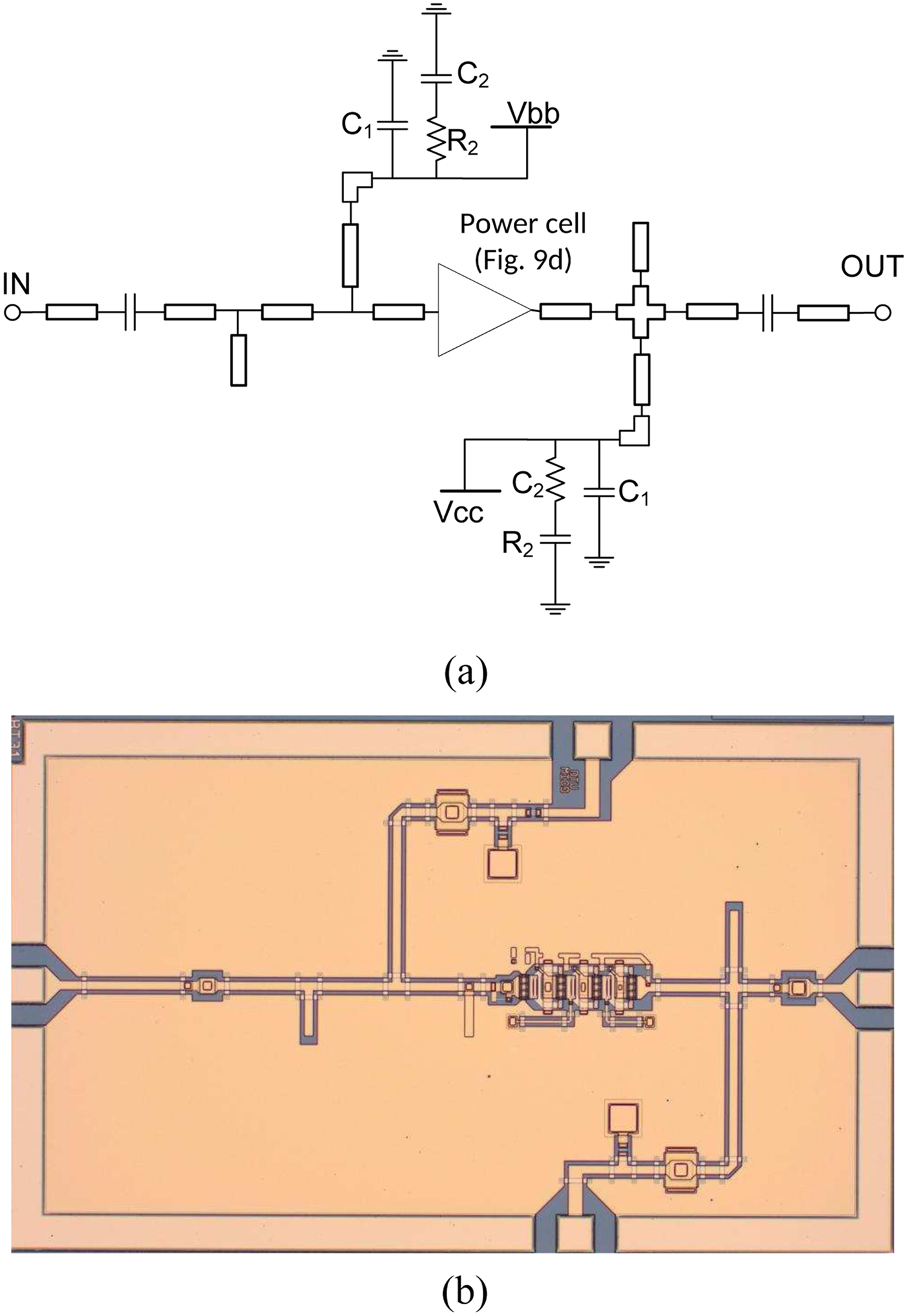
Fig. 16. Schematic (a) and chip microphotograph (b) of the matched four-stacked transistor power cell. The chip size is 2.4 × 1.5 mm2.
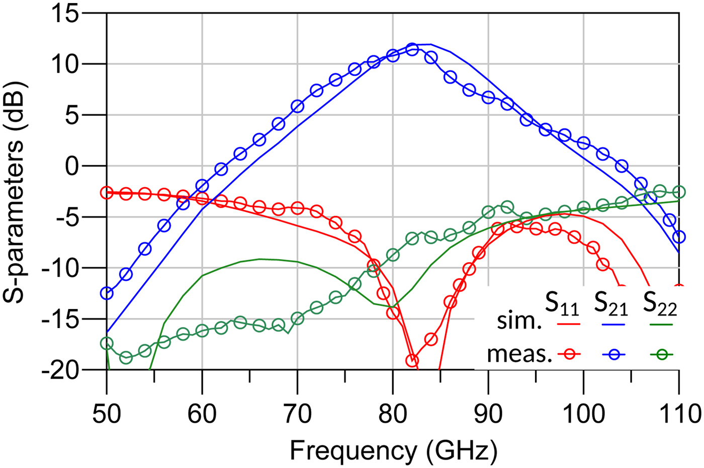
Fig. 17. Simulated and measured S-parameters of the matched four-stacked transistor power cell.

Fig. 18. Simulated and measured power sweep of the matched four-stacked transistor power cell at 81 GHz.

Fig. 19. Output power versus the frequency of the three-stacked and four-stacked MMIC power cells.
Four-way combined three-stacked power amplifier stage
A schematic representation of the designed four-way combined power stage is illustrated in Fig. 20(a). Corporate topologies have been used at the input and output for combining and impedance matching. To prevent odd-mode instabilities, the R odd resistors with a value of 10 Ω are placed midway between adjacent power cells. The collector bias lines have been placed at both sides of the chip to ensure symmetry. The bias voltage V cc has been slightly increased to 6.5 V due to the small voltage drop along the longer bias lines, and a total collector current of 260 mA resulted. The chip microphotograph of the MMIC, whose size is 2.4 × 1.5 mm2, is shown in Fig. 20(b) and the measured and simulated S-parameters are reported in Fig. 21. The 3-dB bandwidth of this power amplifier is from 70 to 95 GHz, 10 GHz larger with respect to the single cell implementation. The peak |S 21 | is 7.8 dB at 83 GHz, 1 dB lower than the simulated one. The insertion loss is better than 10 dB from 67 to 97 GHz. Large-signal measurements have been carried out up to 11 dBm of input power at 84 GHz and are shown in Fig. 22. The highest linear gain is 8.1 dB and is obtained with the input power ranging between −8 and 0 dBm. The limited capabilities of the available measurement setup did not allow to evaluate the performance of the power amplifier in gain compression. At 11 dBm of input power, the output power is 18 dBm and shows little indication of gain compression. Thus the saturated output power is expected to be higher. Simulation results show an output power at the 1-dB compression point of P out,1dB ≈ 21 dBm and a saturated output power of P sat ≈ 22 dBm.

Fig. 20. Schematic (a) and chip microphotograph (b) of the four-way combined three-stacked power stage amplifier. The chip size is 2.4 × 1.5 mm2.

Fig. 21. Simulated and measured S-parameters of the four-way combined three-stacked power stage amplifier.

Fig. 22. Simulated and measured power sweep of the four-way combined three-stacked power stage amplifier at 84 GHz.
Conclusion
In this work, the well-known stacked-transistor topology for power amplifiers design has been extended to InP DHBT technology in an attempt to increase its power performance capabilities at millimeter-wave frequencies, and in particular the E-band. Structured and detailed analysis have been conducted in small- and large-signal regimes, providing guidelines for the design procedure. Limiting factors related to the particular technology have been especially identified in unavoidable layout parasitic effects. In particular, the finite length of the interconnects introduces an undesirable phase misalignment between the collector voltages, resulting in early compression. Three- and four-stacked transistors power cells have been implemented and measured in small- and large-signal operation. At 81 GHz, the saturated output power of the two circuits is comparable, being 15 and 14.9 dBm, respectively. The peak PAE, however, is higher for the three-stacked transistor, 5.2% against 3.8%, because of the lower bias voltage. On the other hand, small-signal gain performances are better for the four-stacked power cell, exhibiting a peak |S 21| of 11.4 dB at 83 GHz against 8.6 dB of the three-stacked one. The three-stacked transistor has been selected as the basic power cell for the implementation of a four-way combined power stage. The measured small-signal gain of this amplifier is 7.8 dB at 83 GHz and the saturated output power is higher than 18 dBm.
Acknowledgments
This work is supported by the European Commission (FP7-People-2013-ITN project IN-POWER, grant #607647).
APPENDIX A. Gain and input admittance of the kth common-base stage
Applying KCL to the equivalent circuit of Fig. 2 gives:
 $$\left\{ \matrix{i_x + i + ic = 0, \hfill {\hskip210pt} {\rm (A.1a)} \cr i_c = i_\mu + i_2, {\hskip225pt}{\rm (A.1b)} \hfill \cr i_1 = i_\mu + i_\pi ,{\hskip224pt} {\rm (A.1c)} \hfill \cr i_x = i_1 + i_2 = 0.{\hskip210pt} {\rm (A.1d)} \hfill} \right.$$
The single currents can be expressed as functions of the node voltages:
 $$i_{c} = g_{m} (v_{b} - v_{x}) + sC_{ceo} (v_{c} - v_{x}),$$
 $$i_\pi=\left(v_{b}-v_{x}\right)/Z_\pi,$$
 $$i_\mu = sC_\mu\left(v_{b}-v_{c}\right),$$
 $$i_{1}=-v_{b}/Z_{b},$$
 $$i_{2}=-v_{c}Y_{L,k},$$
where Z b = R b + 1/(sC k),  $Z_\pi =R_\pi /\!(1 + sC_{\pi }R_{\pi })$, and s = jω. Here we try to express the collector voltage v c as a function of the circuit parameters and the voltage source v x. Using (A.2), (A.4), and (A.6) into (A.1b), the collector voltage can be written as
 $$v_{c} = {\displaystyle{sC_\mu\left(v_{b}-v_{c}\right)-g_{m}\left(v_{b}-v_{x}\right)-sC_{ceo}\left(v_{c}-v_{x}\right)} \over {Y_{L,k}}}. $$
In order to eliminate v b from this expression, we can use the following equivalent relationships:
 $$\left(v_{b}-v_{x}\right)=-\left[{v_b \over Z_b} + sC_\mu\left(v_{b}-v_{c}\right)\right]Z_\pi,$$
 $$\left(v_{b}-v_{c}\right)={\displaystyle{v_{x}Z_{b}-v_{c}\left(Z_{b} + Z_\pi\right)} \over {Z_{b} + Z_\pi + sC_{\mu}Z_{b}Z_\pi}},$$
 $$v_b = {\rm }\displaystyle{{v_xZ_b + v_csC_\mu Z_bZ_\pi } \over {Z_b + Z_\pi + sC_\mu Z_bZ_\pi ,}}$$
so that, after some algebraic manipulation, (A.7) can be rewritten as
 $$v_c = \displaystyle{{\left[ {\left( {sC_\mu + sC_{ceo}} \right)Z_b + \left( {g_m + sC_{ceo}} \right)\left( {1 + sC_\mu Z_b} \right)Z_\pi } \right]} \over \matrix{\left( {Y_{L,k} + sC_{ceo}} \right)\left( {Z_b + Z_\pi + sC_\mu Z_bZ_\pi } \right) \hfill \cr + sC_\mu \left( {Z_b + Z_\pi + g_mZ_bZ_\pi } \right) \hfill} }v_x.$$
In order to find the expression for the input emitter admittance Y in,k, we can consider the equation (A.1d). Using (A.5), (A.6), and (A.10), it can be rewritten as
 $$i_{x} = {\displaystyle{sC_{\mu}Z_{\pi}v_{c} + v_{x}} \over {Z_{b} + Z_\pi + sC_{\mu}Z_{b}Z_\pi}} + v_{c}Y_{L,k}. $$
To find an expression dependent only on v x, we could use (A.11), but for the present case we must have v c = kv x/(k − 1), so we can write (A.12) as:
 $$i_x = {\rm }\left[ {\displaystyle{{sC_\mu Z_\pi (k/(k - 1)) + 1} \over {Z_b + Z_\pi + sC_\mu Z_bZ_\pi }} + \displaystyle{k \over {k - 1}}Y_{L,k}} \right]v_x. $$
which finally yields the expression (3) to calculate the input admittance Y in,k.
 Michele Squartecchia received his B.Sc. and M.Sc. (cum laude) in electronics engineering from the University of L'Aquila, L'Aquila, Italy, in 2010 and 2014, respectively. He is now working towards his Ph.D. at Technical University of Denmark (DTU), Denmark, in collaboration with III-V Lab (Palaiseau, France), a joint lab between Nokia Bell Labs, Thales, and CEA-Leti. In 2018, he joined Bifrost Communications ApS as a circuit designer. His research interests include microwave and mm-wave IC modeling and design for wireless and optical communications.
 Tom K. Johansen received his M.S and Ph.D. degrees in electrical engineering from the Technical University of Denmark, Denmark, in 1999 and 2003, respectively. In 1999 he joined the Electromagnetic Systems group, DTU Elektro, Technical University of Denmark, Denmark, where he is currently an Associate Professor. From September 2001 to March 2002 he was a Visiting scholar at the center for wireless communication, University of San Diego, California, Ca. He has spent several external research stays at the Ferdinand Braun Institute (FBH), in Berlin, Germany. His research areas include the modeling of high-frequency solid-state devices, millimeter-wave, and sub-millimeter-wave integrated circuit design.
 Jean-Yves Dupuy received the Engineer Degree from the Ecole Nationale Supérieure de l'Electronique et de ses Applications (ENSEA, Cergy, France) in 2005, and the Ph.D. Degree summa cum laude from University of Cergy-Pontoise (France) in 2015, both in Electrical Engineering. He joined III-V Lab (Palaiseau, France) in 2005, now a joint lab between Nokia Bell Labs, Thales and CEA-Leti. He is currently leading the High-Speed Electronics Research Department, covering modeling, design, fabrication, packaging, and characterization of high-performance semiconductor devices, integrated circuits and modules, especially in InP DHBT technology, at microwave and millimeter wave frequencies, aiming at pioneering high-speed analog and digital interfaces in performance-critical optoelectronic and RF systems. Dr. Dupuy has been a participant to the 2013 EU-US Frontiers-Of-Engineering Symposium and a co-recipient of the IET 2017 Electronics Letters Premium Award. He has co-authored more than 100 scientific publications and holds two patents.
 Virginio Midili received his B.Sc. in Electrical Engineering from Politecnico di Milano, Milan, Italy, in 2010 and his M.Sc. in Micro and Nanotechnology from Aalto University, Helsinki, Finland, in 2012. He received an industrial Ph.D. Degree from the Technical University of Denmark working in collaboration with Nokia Bell-Labs, III-V Lab in France. His research focused on the optimization of InP DHBT transistors for power amplifiers at mm-wave frequencies.
 Virginie Nodjiadjim received the Ph.D. degree in electronic engineering from the University of Lille I, Lille, France, in 2009. In 2009, she joined Alcatel-Thales III-V Labs (currently III-V Lab), Bell Labs, Marcoussis, France, as a Research Engineer, where she has studied compound semiconductor heterojunction bipolar transistors. She is currently in charge of the InP DHBT development: structure and design optimization, characterization, and modeling.
 Muriel Riet received the Ph.D. degree in electronic engineering from the University of Paris XI, Paris, France, in 1985. In 1985, she joined CNET, a research center of France Telecom, where she has studied compound semiconductor heterojunction bipolar transistors. Since 1998, she has been in charge of InP HBT technology for high-bit-rate optical communications up to 40 Gb/s in the III-V Lab, Marcoussis, France.
 Agnieszka Konczykowska is in charge of microelectronic design activity at III-V Lab, Bell Labs, Thales Research and Technology and CEA/Leti joint laboratory, Marcoussis in France. She is presently an active researcher in the domain of components and circuits for telecommunication systems, in particular for optical and wireless communications. She is author and co-author of over 200 publications and six patents. From 1995 to 1999, she was the president of European Circuit Society. She is an IEEE Fellow.


