


I. INTRODUCTION
High-frequency LC-tank is a well known circuit of inductor and capacitor, no expansion oscillators are key components of widely adopted architectures for wireless communication systems. Their performance is crucial in many applications such as wireless transceivers, modulators, and radar systems. Furthermore, the availability of larger bandwidths at higher frequencies, such as the 60 GHz frequency band, combined with the growing demand for higher data rates makes it necessary to design such oscillators for operation closer to the limits of the available technology. Several kinds of LC-tank oscillators can be found in the literature, such as the cross-coupled and the Colpitts oscillators. Even though it was shown in [Reference Hajimiri and Lee1] that the Colpitts oscillator outperforms the cross-coupled oscillator in terms of phase noise, which makes it a better choice, the simpler architecture of the cross-coupled oscillator makes it a more favorable choice in applications where phase noise is not of high concern. Therefore, it is very beneficial to estimate the frequency limits of this topology to perform as an oscillator. In [Reference Barghouthi and Ellinger2], an expression for the negative resistance of Colpitts oscillators at high frequencies was derived. In [Reference Li and Rein3], Barhausen's criteria were used to derive expressions for the oscillation conditions of Colpitts oscillator. In [Reference Mansour, Mansour and Mehorta4], large signal analysis for Complementary Metal Oxide Semiconductor (CMOS) cross-coupled oscillators was presented. Unfortunately, a high-frequency analysis of the negative conductance of HBT cross-coupled oscillators, to the knowledge of the authors, has never been considered. Even though, such analysis can bring a lot of insight into the frequency limits of the topology. In this paper, we derive analytical expressions to show how the HBT transistor parasitics impose a limit on the ability of the cross-coupled topology to oscillate at higher frequencies. This is shown by deriving an improved estimation of the negative conductance, which is valid at high frequencies, and using it to find an expression for the frequency at which the negative conductance crosses zero.
II. CIRCUIT ANALYSIS
The cross-coupled oscillator architecture is shown in Fig. 1. In order to understand its behavior at high frequencies, the negative conductance approach is used for the circuit analysis. The differential circuit small signal model is shown in Fig. 2. First, the circuit is analyzed by considering a short circuit in-place of C m, and then, the effect of C m is taken into account.

Fig. 1. Cross-coupled VCO with C bc compensation.

Fig. 2. Cross-coupled VCO small signal model with C bc compensation.
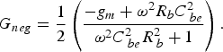
The negative conductance of the oscillator can be defined as
In the literature [Reference Ellinger5–Reference Jeong, Choi and Yang7], equation (2) is commonly used in estimating the negative conductance G neg of the oscillator:
where g m is the transistor trans-conductance.
Unfortunately, this is not valid for high frequencies, due to the effect of transistor parasitics, such as the base resistance R b, the base emitter capacitance C be, the base collector capacitance C bc, the collector resistance R c (not shown in Fig. 2), and the emitter resistance R e. Even at low frequencies and small transistor size, the estimation is inaccurate due to R e. In the following, the effect of the parasitics and C m is analyzed:
1. The effect of R e: by neglecting all other parasitics and replacing C m with a short circuit, equation (3) can be derived. It can be concluded that R e reduces G neg by a factor of
 for low frequencies.
(3)
for low frequencies.
(3)2. The effect of C be and R b: equation (3) predicts a flat negative conductance over the whole frequency range, in reality the magnitude of the negative conductance decreases with frequency. This is explained by analyzing the circuit taking into account C be and R b, while neglecting the other effects. As a result, equation (3) has to be modified to
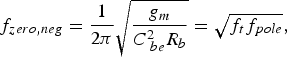
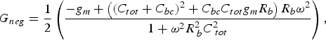
(4)As can be noticed, a pole that decreases the magnitude of the negative conductance appears in the equation. The pole-frequency is(5)The G neg crosses zero at a frequency of(6)where f t is the transit frequency of the technology.3. Taking the effect of C be, R b, and C bc into account, the expressions for G neg and f pole are further modified as
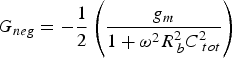
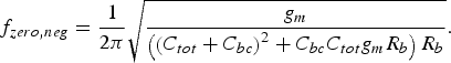
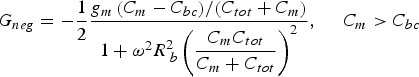
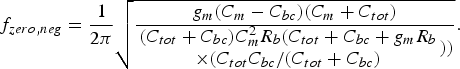
(7)(8)where C tot = C be + C bc. From (7), an estimation of the upper limit of the negative conductance can be derived as a function of the technology parameters. The designer can use such an upper limit to have a first judgment about the feasibility of using the cross-coupled oscillator for the target frequency, by comparing the tank losses with the upper limit. The upper limit of G neg is(9)and the G neg crosses zero at a frequency of(10)4. The effect of feedback capacitance on the G neg of the oscillator: in order to boost the ability of a cross-coupled oscillator to give negative conductance at higher frequencies and to decouple the bias from the outputs, a capacitor C m is commonly inserted in the feedback path to eliminate the effect of C bc, as shown in Fig. 1. Circuit analysis shows that the pole-frequency shifts to a frequency of
(11)The upper limit of negative conductance is(12)and the G neg crosses zero at a frequency of(13)
III. SIMULATIONS
In this section, the analytical derivations are validated and illustrated by simulations, which rely on the compact model of the HBT of a commercially available technology. The simulation results correspond to a transistor with the following parameters: R b = 17 Ω, C bc = 18 fF, C be = 195 fF, R e = 3.2 Ω, R c = 11.4 Ω, and g m = 257 mS. However, the analysis results were successfully validated for several other transistor sizes, all available in the same integrated circuit (IC) technology. As can be noticed in Fig. 3, f zero,neg takes all effects into account at around 65 GHz. When only C be and R b are taken into account (equation (6)) the estimated f zero,neg is 100 GHz, when C bc effect is added (equation (10)), the estimated f zero,neg is 76 GHz.

The effect of C m was also evaluated. As can be noticed from Fig. 4, where the conductance of the circuit is plotted versus frequency for different values of C m, using C m = 17 fF ≅ C bc generates positive values for the conductance, as closely predicted by (12). Using larger values for C m will finally bring the conductance to the short-circuited case, as in (7).

Fig. 4. The effect of C m on the negative conductance of the cross-coupled oscillator.
It can also be deduced that, even though using C m improves the magnitude of negative conductance at higher frequency, the magnitude can still be low and insufficient for compensating the tank losses. In addition to negative conductance simulations, transient simulations were performed to support the conclusions made in this section. An ideal inductor was used to resonate with the capacitance, which corresponds to the imaginary part of Y in. The inductor was scaled to the minimum value that allows oscillation (corresponding to the highest frequency of oscillation). The following two cases were considered:
1. The short circuited C m: as can be seen in Fig. 5 the oscillation frequency corresponds to the predictions of the negative conductance.
2. C m = 42.5 fF: (Fig. 6).

Fig. 5. Simulated highest frequency of oscillation (64 GHz).

Fig. 6. Simulated highest frequency of oscillation (98 GHz).
IV. CONCLUSION
The paper brings more insight into the frequency limits of the cross-coupled oscillator at high frequencies than already available. An upper bound of the negative conductance was derived, which helps the designer to check for the suitability of the architecture at the target frequency and enables quick technology evaluation and comparison. A maximum frequency f zero,neg at which the circuit can provide negative conductance is given in (10) and (13). It should be noted that even though oscillation at frequencies higher than f zero,neg is not possible, the magnitude of the negative conductance might be too low to sustain oscillation at frequency below this upper limit. On the other hand, the presented results provide a simple expression of the negative conductance values available as a function of the target frequency of operation. It was also shown that choosing C m smaller than C bc compromises the ability of the circuit to present negative conductance to the resonant tank and is thus incompatible with oscillation.
ACKNOWLEDGEMENT
This work was supported by the German Ministry of Education and Research in the framework of project “Enablers for Ambient Systems, part A” (EASY-A).
APPENDIX A
In this appendix, equations (7)–(10) are derived. Analyzing the circuit in Fig. 2 using nodal analysis in the Laplace domain generates two different equations, one for each node in the circuit (only two nodes are needed because the circuit is symmetric). In this appendix, the capacitor C m is replaced by a short circuit and R e is neglected.
1.
node:
(A.1)which simplifies to(A.2)2.
node:
(A.3)which simplifies to(A.4)
By substituting (A.4) into (A.2) and solving for Y in, equation (A.5) is found

By substituting jω instead of s in (A.5) and separating the equation into the real and imaginary parts, G neg can be calculated, as given in (7). By separating (7) into two parts, a negative and a positive part, the upper limit of the negative conductance can be found by using the negative part, which is given in (9). In order to derive (10), equation (7) is set to zero and solved for the frequency, f zero,neg can then be found.
APPENDIX B
In this appendix, equations (11)–(13) are derived. Analyzing the circuit in Fig. 2 by using nodal analysis in the Laplace domain generates two different equations, one for each node in the circuit (only two nodes are needed because the circuit is symmetric). In this appendix, Cm is taken into account and R e is neglected.
1.
node:
(B.1)where.2.
node:
(B.2)which simplifies to(B.3)
By eliminating ![]() using (B.1) and (B.2), equation (B.4) is found
using (B.1) and (B.2), equation (B.4) is found
By substituting (B.3) into (B.4) and solving for Y in, equation (B.5) is found.
By substituting jω instead of s in (B.5) and separating the equation into the real and imaginary parts, G neg can be calculated, as given in (B.6).
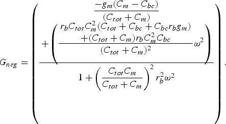
By separating (B.6) into two parts, a negative and a positive part, the upper limit of the negative conductance can be found by using the negative part, which is given in (12). In order to derive (13), equation (B.6) is set to zero and solved for the frequency, f zero,neg can then be found.
 Atheer Barghouthi received his B.Sc. in electrical engineering in 2004 from Birzeit University in Palestine with distinction and received his M.Sc. in microelectronics and microsystems from Hamburg University of Technology in 2008 with distinction. Currently, he works for his Ph.D. as a scientific research employee in Dresden University of technology in the field of RF circuit design.
 Udo Jörges was born in Steinach (Thuringia), Germany, in 1952. He received the Diploma degree in electrical engineering, Ph.D. degree, and Habilitation degree in electrical engineering from the Dresden University of Technology, Dresden, Germany, in 1975, 1979, and 1985, respectively. Since 1998, he has been an Associate Professor, and since 2006, he is with the Chair for circuit design and network theory at Dresden University of Technology. His main research interests are in the field of circuit theory and the design of analog ICs.
 Corrado Carta was born in Cagliari, Italy. He received the Master degree in Electrical Engineering from the University of Cagliari, Italy, in 2000 and the Ph.D. degree from the Swiss Federal Institute of Technology (ETH) Zurich, Switzerland, in 2006. From July 2000 to February 2006, he was with the Microwave Electronics Group of ETH Zurich, where his main research interests were in the field of silicon-based RFIC design for wireless communications. From April 2006 to May 2008, he was with the High-Speed Electronics Group at the Electrical and Computer Engineering Department of the University of California, Santa Barbara, where his research work focused on the design of silicon-based integrated-circuits for very large mm-wave phased arrays. In June 2008, he joined Sonos Inc., where he led the RF and compliance team, involved in the development and characterization of the wireless interface of new and existing products. In March 2010, he joined the Chair for Circuit Design and Network Theory at TU Dresden, where he is currently leading the mm-wave IC design group.
 Frank Ellinger was born in Friedrichshafen, Germany, in 1972. He graduated in electrical engineering (EE) in 1996 from the University of Ulm, Germany. He received an MBA and a PhD degree in EE from the ETH Zürich (ETHZ), Switzerland, in 2001, and the habilitation degree in high frequency circuit design from the ETHZ in 2004. Since August 2006 he is a full-time professor and head of the Chair for Circuit Design and Network Theory at the Dresden University of Technology, Germany. Currently, he is member of the management board and coordinator of the communications area in the German excellence cluster project Cool Silicon. From 2001 to 2006, he was head of the RFIC design group of the Electronics Laboratory at the ETHZ, and a project leader of the IBM/ETHZ Competence Center for Advanced Silicon Electronics hosted at IBM Research in Rüschlikon. Prof. Ellinger has been coordinator of the EU funded projects RESOLUTION and MIMAX. He published more than 170 refereed scientific papers, most of them IEEE journal contributions, and three patents. Prof. Ellinger authored the lecture book “Radio Frequency Integrated Circuits and Technologies” published by Springer. He was elected by the IEEE MTT S as IEEE Distinguished Microwave Lecturer for 2009–2011.


