I. INTRODUCTION
New generations of wireless communication systems require data transmission rates that are constantly increasing. Modulation schemes needed to improve spectral efficiency result in radio frequency (RF) signals having large peak to average power ratios (PAPR). In order to ensure signal integrity, transmitters must meet stringent linearity specifications that put a challenging dilemma on DC consumption reduction and electrical efficiency enhancement of power amplifiers. Basically, linear amplification of non-envelope constant RF signals consists in using oversized PAs that operate at output power back off. Doing so, linearity performances are reached at the detriment of poor efficiency performances.
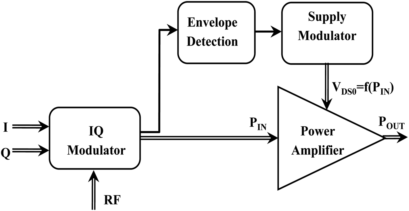
Envelope tracking (ET) is an interesting approach to overcome efficiency versus linearity antagonism. The quite simple idea is to save DC consumption of power amplifiers at backed off power levels by lowering dynamically the drain bias voltage synchronously with the instantaneous envelope decrease of the RF input signal. For that purpose, an envelope tracking power amplifier (ETPA) includes a drain bias modulator based on the use of a DC/DC converter to modulate drain bias versus instantaneous envelope variations of the input RF signal as illustrated in Fig. 1.

Fig. 1. Envelope tracking amplifier block diagram.
The output of the DC/DC converter supplies the drain port of the power amplifier with a time-varying voltage following a drain bias trajectory having a generic shape as illustrated in Fig. 2.
Fig. 2. Example of continuous and MET implementation.
Drain bias trajectories required in ETPA can be done either in a continuous way (CET: continuous ET) or according to a discrete multilevel representation (MET: multilevel ET). In this work, a discrete four-level ET implementation is considered.
The drain bias modulator must be wideband and highly efficient, otherwise it impacts to much the overall efficiency and any implementation of ETPA architectures loses its interest. The design of wideband, high-power and efficient supply modulators still remains the cornerstone for adaptive, linear and efficient power amplification. GaN devices appear to be the best potential candidates to face this challenge. A lot of works, proposing original supply modulator topologies, have been reported during the past years [Reference Kim1–Reference Kanbe10]. One of the most popular architecture is the hybrid switching amplifier (HSA) described in [Reference Kimball2, Reference Aitto-oja6–Reference Kanbe10].
This paper proposes a novel supply modulator topology, addressing the implementation of ETPA in base stations. The work reported here concerns the design and implementation of a discrete multilevel supply modulator. It is based on a novel high-speed and high-power GaN switching circuit that has not been yet reported to our knowledge.
In Section II, the core switching cell is presented. Static and dynamic behaviors are described. Fast transients and short switching times are highlighted.
Section III deals with the design of the supply modulator using an appropriate combination of the proposed switching cells. Some experimental results are discussed and demonstrated the potentialities of the proposed modulator.
To conclude further investigations are mentioned.
II. THE PROPOSED GAN HEMT SWITCHING CELL
A) The proposed core switching cell
The switching circuit topology is based on the use of two HEMT transistors as shown in Fig. 3.
Fig. 3. Schematic representation of the core switching cell.
For proper operation, transistor T 2, which is the main switching device delivering power to the load, is necessarily a normally-on transistor driven with a negative gate–source voltage. Transistor T 1 acts as a driver and controls the current in resistor R 2. T 1 and T 2 are power GaN devices of different sizes depending on the required output current as explained later in the paper.
The core switching circuit in Fig. 3 behaves like a threshold comparator with two stable ON/OFF states. Resistor R 1 ensures stability. Resistor R 2 enables the self-biasing of transistor T 2 during its OFF state.
ON State of the cell, ideally V OUT = V DD:
Transistor T 1 is pinched-off. No current flows across resistors R 1 and R 2. The gate–source voltage V GS2 is equal to zero. Transistor T 2 state is ON and its drain–source impedance is R ON. The output voltage V OUT is nearly equal to V DD, neglecting the dropout voltage due to R ON.
OFF State of the cell, ideally V OUT = V P:
Transistor T 1 state is ON. There is now a current flowing across resistors R 1 and R 2. Transistor T 2 reaches a self-biased point at a gate–source voltage V GS2 close to its pinch-off voltage V P. Transistor T 2 is almost in an OFF state and V OUT voltage is very close to V P.
Dynamic switching characteristics
The analysis of switching transients is a key aspect to optimize maximum switching frequency and consequently the intrinsic speed capability of the proposed circuit for its use in wideband ETPA. Figure 4 shows the equivalent circuit used for the theoretical analysis of the circuit behavior. The goal here is to evaluate the dependence of the switching speed as a function of intrinsic capacitances of the main transistor T 2. The simplified model of T 2 is composed of two main capacitances C GS and C DS and a current controlled source I D. Transistor T 1 is considered here as an ideal switch modeled by a serial resistor R T1ON or R T1OFF, depending on its ON/OFF state.
Fig. 4. Simplified schematic for theoretical analysis.
The current source I D of T 2 is described by the piecewise equation (1) which is representative of the operating trajectory in the (I D, V GS) plane (see Fig. 5). The gate–source voltage V GS is bounded between V GSOFF and V GSON, so that there is no need of defining an equation for V GS values lower than pinch-off value −V p. The ideal output load line in the (I D, V DS) plane, plotted in Fig. 5, is bounded between V DSON voltage at low V DS and V DSOFF voltage at high V DS. These ideal trajectories represent the static operation of the circuit. So, they depend only on resistive and convective intrinsic elements of transistors, there are no specific assumptions on capacitive elements. Concerning device T 1, the ON/OFF resistors R T1ON and R T1OFF slightly impacts on V GSON and V GSOFF steady-state values. The resistor R ON of device T 2 impacts on the value of V DSON voltage and must be minimized to avoid a too important voltage drop at ON state.
 $$\left\{{\matrix{ {I_D=I_{DSS} \left({1+\displaystyle{{V_{GS} } \over {V_p }}} \right)} & {{\rm if}\, - V_P \lt V_{GS} \lt - V_K } \cr {I_D=\displaystyle{{V_{DD} } \over {R_L+R_{ON} }}} & {{\rm if}\, - V_K \lt V_{GS} \lt 0} \cr } } \right.$$
Fig. 5. Linear piecewise characteristic I D = f(V GS) of transistor T 2 and output ideal load line.
When switching from OFF to ON states, the current I D reaches its maximum value I DMAX (i.e. ON state value) at V GS equal to the knee voltage −V K. The value of V K in equation (2) is obtained by combining equations (1) at the point V GS = −V K.
 $$V_K=V_P \left({1 - \displaystyle{{V_{DD} } \over {\lpar R_L+R_{ON} \rpar I_{DSS} }}} \right).$$
For V GS values between –V P and –V K, the current source I D is described with the simplified linear equation of a transistor working in its saturation area. For V GS values between –V K and 0, the transistor operates in the Ohmic area, and for convenience here, the drain current is assumed to be constant and independent of V GS voltage. This particular trajectory, proper to this switch mode operation, has been validated by transient simulations achieved by using a complete non-linear transistor model.
Coming back to circuit schematic of Fig. 4 and going on with the piecewise analytical description of I D current, two second-order differential equations of V GS can be then derived. In order to simplify calculations, we use equations truncated to the first order (see equations (3) and (4)).
 $$\eqalign{{R_L}{I_{DSS}} &+ \left( {1 + \displaystyle{{{R_{T1}} + {R_1} + {R_L}} \over {{R_2}}}{\mkern 1mu} + \displaystyle{{{R_L}{I_{DSS}}} \over {{V_P}}}} \right){V_{GS}}(t{\rm )} \cr & + \left( \left( {{R_{T1}} + {R_1}} \right) {\left[ {{C_{GS}} + {C_{GD}}\left( {1 + \displaystyle{{{R_L}{I_{DSS}}} \over {{V_P}}} + \displaystyle{{{R_L}} \over {{R_2}}}} \right)} \right] + {R_L}{C_{GS}}} \right)\displaystyle{{d{V_{GS}}{\rm (}t{\rm )}} \over {dt}} = 0\quad {\rm if}{\mkern 1mu} - {V_P}{\rm \lt }{V_{GS}}{\rm \lt } - {V_K}{\rm ,}\; }$$
 $$\eqalign{\displaystyle{{R_L V_{DD} } \over {R_L+R_{ON} }} &+\left({1+\displaystyle{{R_{DS1}+R_1+R_L } \over {R_2 }}\, } \right)V_{GS} \lpar t\rpar \cr & +\left({\lpar R_{DS1}+R_1 \rpar \left[{C_{GS}+C_{GD} \left({1+\displaystyle{{R_L } \over {R_2 }}} \right)} \right]+R_L C_{GS} } \right) \displaystyle{{dV_{GS} \lpar t\rpar } \over {dt}}=0\comma \; \quad {\rm if}\, -\! V_K\lt V_{GS}\lt 0.}$$
The initial value V GSOFF is determined by solving equation (3) considering the steady-state (d/dt = 0) and taking R T1 = R T1ON.
 $$V_{GSOFF}=\displaystyle{{ - R_L I_{DSS} } \over {\left({\displaystyle{{R_{T1ON}+R_1+R_L } \over {R_2 }}+\displaystyle{{R_L I_{DSS} } \over {V_P }}+1} \right)}}.$$
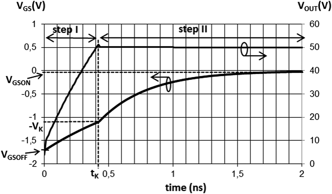
Starting from this initial value, the OFF–ON transition is analyzed using equations (3) and (4). The resolution of equations (3) and (4) leads to an OFF–ON transient composed of two steps as shown in Fig. 6. The first step, in which the output voltage V OUT is established, has a duration t K. Then, during the second step, the V GS voltage continues to increase up to V GSON final value.
Fig. 6. V GS and V OUT time waveforms during OFF → ON transition for R 1 = 8 Ω, R 2 = 35 Ω, R L = 80 Ω, V DD = 50 V, R ON = R T1ON = 2 Ω, R T1OFF = 100 KΩ, I DSS = 1.6 A, V P = 1.8 V, C GS = 10 pF, C GD = 0.25 pF.
The expression of t K is given in equation (6) where τ 1 and V 0 are constants derived from solving equation (3).
 $$t_K \, =- \tau _1 \ln \left[{\displaystyle{{V_K+V_0 } \over {V_0 - V_{GSOFF} }}} \right]\comma$$
where
 $$V_0=\displaystyle{{ - \, R_L I_{DSS} } \over {1+\displaystyle{{R_{T_1 OFF}+R_1+R_L } \over {R_2 }}+\displaystyle{{R_L I_{DSS} } \over {V_P }}}}$$
and
 $$\tau _1=\displaystyle{{\left({R_{T_1 OFF}+R_1+R_L } \right)C_{GS}+\left({R_{T_1 OFF}+R_1 } \right)C_{GD} \left({1+\displaystyle{{R_L I_{DSS} } \over {V_P }}+\displaystyle{{R_L } \over {R_2 }}} \right)} \over {1+\displaystyle{{R_{T_1 OFF}+R_1+R_L } \over {R_2 }}+\displaystyle{{R_L I_{DSS} } \over {V_P }}}}.$$
In the ideal case where R T1OFF tends to infinity and R 1 to zero, the expression of t K reduces to equation (9). This expression highlights the dependence of the switching time t K as a function of intrinsic capacitances of T 2. A simple numerical evaluation shows that the contributions of C GS and C GD capacitances are almost the same. The switching speed is directly linked to the amount of electrical charges stored in the capacitances. Although C GD is smaller than C GS, it is charged with V GD voltage, which is about 20 times higher than V GS voltage. Finally, these two capacitances store almost identical charges.
Equation (9) also shows that the switching time t K is minimized if −V K tends to V GSOFF. This can be done by increasing I DSS, i.e. by oversizing T 2 comparatively to the required I DMAX current.
 $$t_K=\left({R_2 C_{GS}+R_2 C_{GD} \left({1+\displaystyle{{R_L I_{DSS} } \over {V_P }}+\displaystyle{{R_L } \over {R_2 }}} \right)} \right)\ln \left[{\displaystyle{{ - V_K } \over {V_{GSOFF} }}} \right].$$
The second step of the OFF–ON transition is done by solving equation (4). This step is characterized by a time constant τ 2 (equation (10)) and the V GSON steady-state value (equation (11)). In this step, V OUT voltage is already established and we can consider that the cell is switched on, the time constant τ 2 affects only V GS voltage.
 $$\tau _2=\displaystyle{{\left({R_{T_1 OFF}+R_1+R_L } \right)R_2 C_{GS}+\left({R_{T_1 OFF}+R_1 } \right)R_2 C_{GD} \left({1+\displaystyle{{R_L } \over {R_2 }}} \right)} \over {R_{T_1 OFF}+R_1+R_2+R_L }}\comma$$
 $$V_{GSON}=- \displaystyle{{R_L } \over {\left({R_L+R_{ON} } \right)}}\displaystyle{{R_2\, V_{DD} } \over {\left({R_{T_1 OFF}+R_1+R_L+R_2 } \right)}}.$$
A similar theoretical analysis for the ON–OFF transition is performed and it shows that the ON–OFF switching time is at least five times lower than t K, depending on component values.
To sum up, the switching speed of the cell is limited by the OFF–ON switching time (t k). It can be minimized by using large size power transistors with small pinch-off voltages.
III. IMPLEMENTATION OF THE ET MODULATOR
A) Schematic and performance analysis of the MET modulator
The block diagram of the proposed discrete multilevel supply modulator is given in Fig. 7. It consists in switching N DC supplies having different V DDi voltage values to a common load R L. For that purpose the output of each switching cell is connected to the load through a fast switching diode. Depending on the required voltage V DDi across the load, only one switching cell among N is active at a same time and feeds the load with current flowing from DC bias V DDi. Diodes ensure isolation between the output of the activated cell and the output of all other inactivated cells. Otherwise there would exist a current sinking at the output of inactivated cells.
Fig. 7. Block diagram of the N cells multilevel modulator.
Let us now consider a theoretical analysis of the supply modulator DC consumption. In the following, power efficiency performances are calculated during the steady states and power losses occurring during voltage transients are not taking into account. An example of ideal discrete multilevel output voltage waveforms is given in Fig. 8, corresponding to the combination of seven switching cells. As mentioned earlier that only one switching cell is in an ON state, whereas all the others are in OFF states. It is also assumed that the activation of each cell follows a uniform density probability. Considering N cells and a recurrence time equal to Nτ, each switching cell is activated during a time τ and is inactivated during a time equal to (N − 1)τ. Each input control signal, noted Ini in Fig. 7, has a duty cycle λ = 1/N.
Fig. 8. Example of V OUT time waveform and fourth cell input signal (N = 7).
Considering the basic operation of each switching cell described in the Section II.B and following assumptions mentioned above, the expression of the average DC supply power and the average output power of the supply modulator are given respectively in equations (12) and (13).
 $${P_{SUPtot}} = \sum\limits_{i = 1}^N {{P_{SUPi}}} = \displaystyle{1 \over N}\sum\limits_{i = 1}^N {\left( {\displaystyle{{V_{DDi}^2 } \over {{R_L} + {R_{ON}}}} - \left( {N - 1} \right)\displaystyle{{{V_{GSOFF}}{V_{DDi}}} \over {{R_2}}}} \right)} ,$$
 $$P_{OUT}=\displaystyle{1 \over N}\sum\limits_{i=1}^N {\displaystyle{1 \over {R_L }}\left({\displaystyle{{R_L } \over {R_L+R_{ON} }}V_{DDi} - V_{Diode} } \right)^2 } .$$
The supply modulator efficiency η is given equation (14).
 $$\eta=\displaystyle{{P_{OUT} } \over {P_{SUPtot} }}=\displaystyle{{\sum\limits_{i=1}^N {\displaystyle{1 \over {R_L }}\left({\displaystyle{{R_L } \over {R_L+R_{ON} }}V_{DDi} - V_{Diode} } \right)^2 } } \over {\sum\limits_{i=1}^N {\left({\displaystyle{{V_{DDi}^2 } \over {R_L+R_{ON} }} - \left({N - 1} \right)\displaystyle{{V_{GSOFF} V_{DDi} } \over {R_2 }}} \right)} }}.$$
with V GSOFF expression given in equation (5).
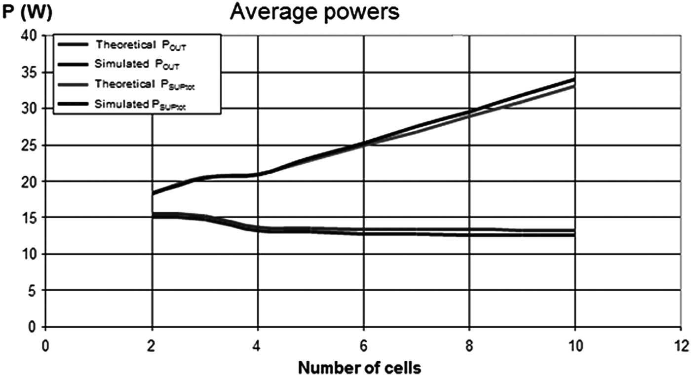
DC powers (P SUPtot) and output powers (P OUT) as well as efficiency are plotted versus the number of cells respectively in Figs. 9 and 10. Minimum and maximum supply voltages are respectively V DD1 = 14 V and V DDn = 50 V. N intermediate values V DDi are uniformly distributed in the range V DD1 to V DDn.
Fig. 9. Average powers versus the number of cells for R 1 = 8 Ω, R 2 = 90 Ω, R L = 80 Ω, R ON = 2 Ω, I DSS = 1.6A, V P = 2.1 V.
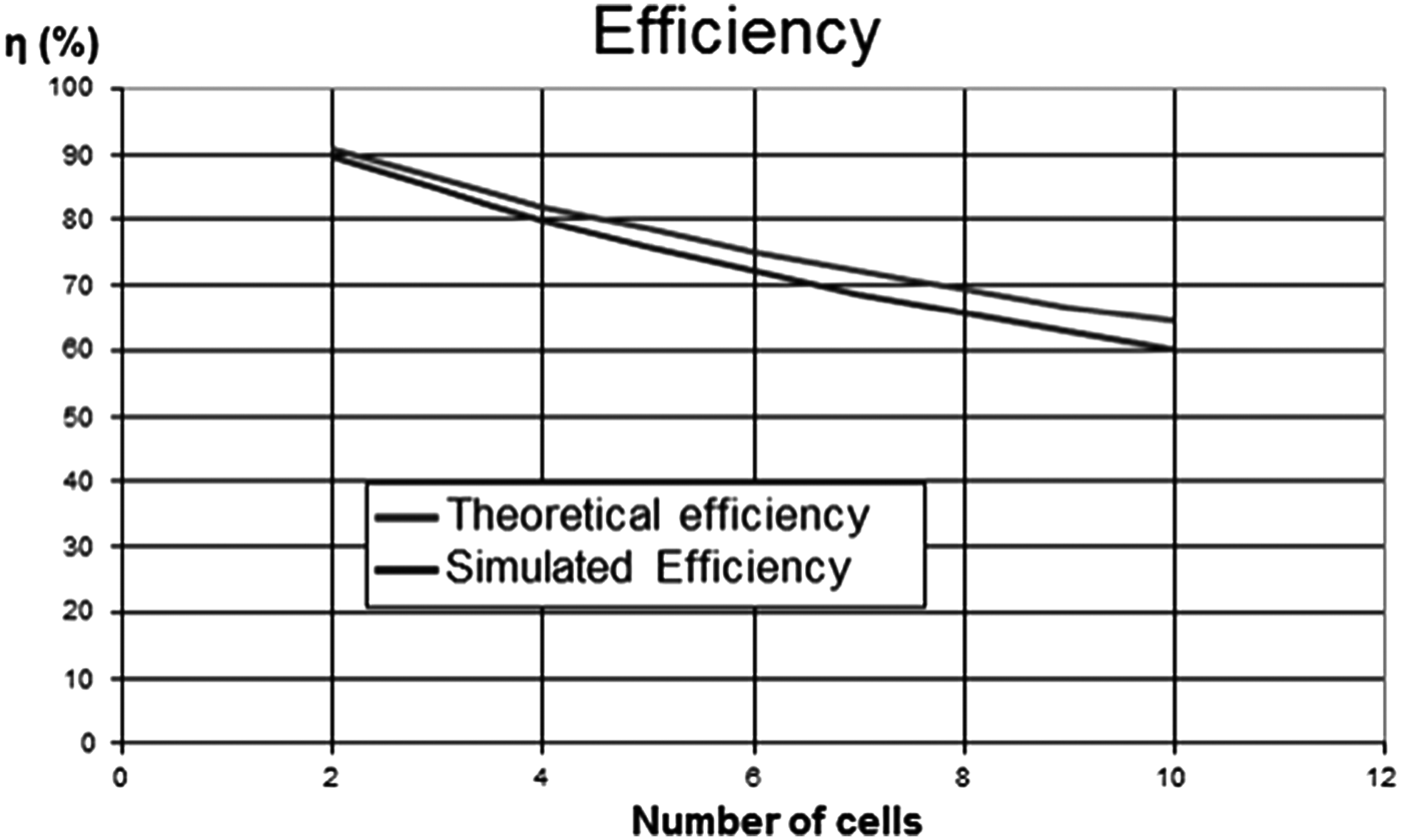
Fig. 10. Efficiency versus the number of cells for R 1 = 8 Ω, R 2 = 90 Ω, R L = 80 Ω, R ON = 2 Ω, I DSS = 1.6 A, V P = 2.1 V.
Analytical calculations are compared to ADS simulation results. ADS transient simulations are performed by taking a recurrence time Nτ of 200 ns. For simulation purpose, a non-linear model of a 6 × 400 µm GaN HEMT from III–V Lab foundry was used.
We can observe a good agreement between simulated and theoretical results. The simulated curves indicate slightly lower performances because they take into account power losses during transients.
When the number of cells increases, the output power remains quasi-constant, while the DC supply power increases, leading to efficiency decrease. In fact, inactive cells consume some energy. As the number of inactive cells increases, the corresponding dissipated power increases, inducing a reduction of the efficiency. Consequently, according to our experience, we can consider that an optimal number of switching cell is of the order of four.
In Fig. 10, the theoretical efficiency curve is the optimal curve for this set of values. The simulated curve is slightly lower because it takes into account transition losses.
IV. DESIGN AND IMPLEMENTATION
A) Four-level MET modulator
This part is devoted to the implementation of a four-cell supply modulator as presented in Fig. 11. T 1 and T 2 transistors are RF GaN HEMT's on Si substrate from Nitronex. Their nominal output powers are 5 W (NPTB00004) for T 1 and 45 W (NPT1004) for T 2. Maximum currents are respectively 1.3 and 9.5 A.
Fig. 11. Block diagram of the complete MET modulator (four cells).
The input signals C 1,…,4 (Fig. 11) are digital signals coming from an FPGA. Driver blocks are realized with fast 1 GHz bandwidth LMH6703 Operational Amplifiers from Texas Instruments.
These drivers allow us to:
– Match voltage levels between FPGA outputs and T 1 transistor gate ports. FPGA output voltages are between 0 and 3 V and signal driving T 1 gates must be between 0 and −3 V.
– Supply T 1 transistor gates at high frequency with sufficient current.
– Isolate FPGA outputs from the high-power switching circuit.
Silicon carbide Schottky diodes CSD01060 from CREE are used. These diodes present negligible recovery time and a sufficient current handling (5 A). They are not limiting components in terms of switching speed but it is necessary to take into account their DC consumption in the whole power efficiency budget.
The photography of the built-in four-level MET modulator is depicted in Fig. 12.
Fig. 12. Photography of the MET modulator.
B) MET modulator characterization setup
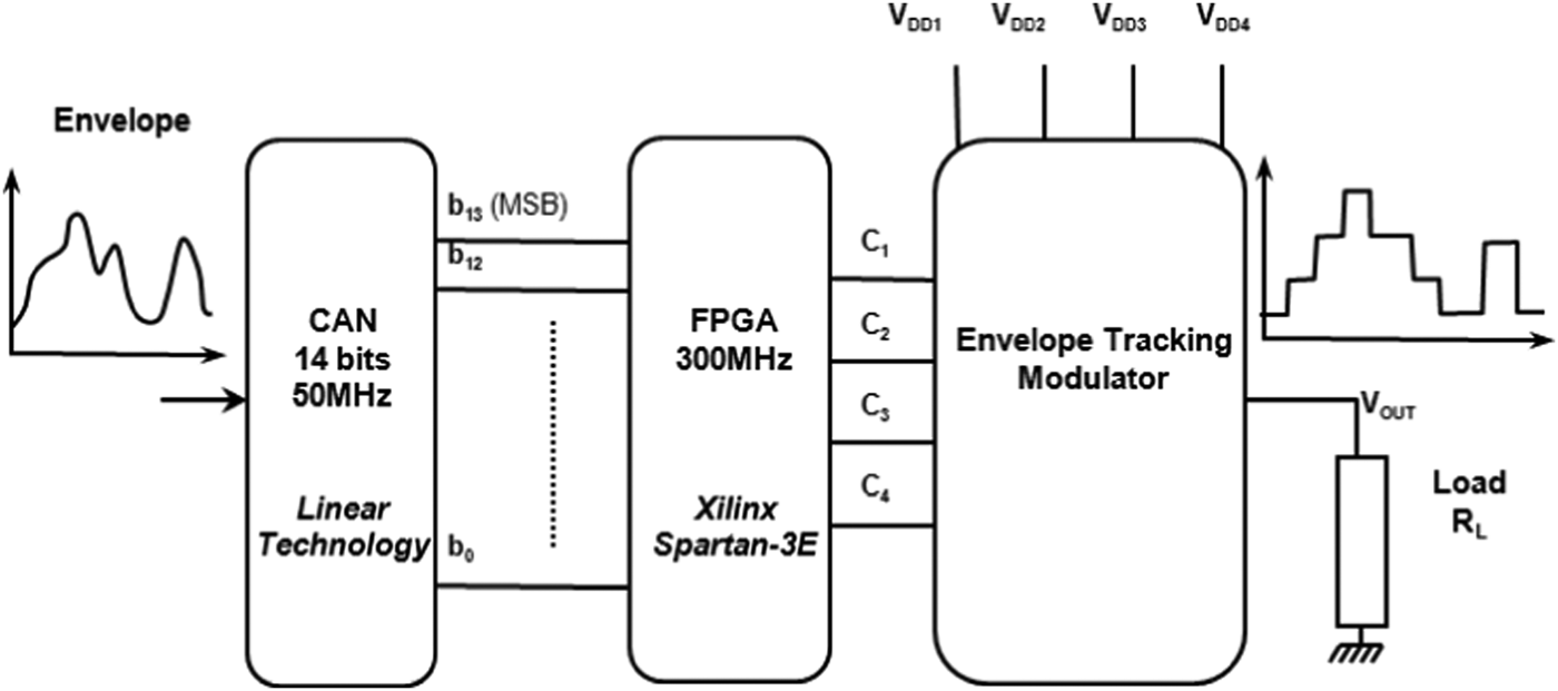
The overview of the complete ET system is presented in Fig. 13. The input envelope signal is digitized by using a 14 bits −50 MHz ADC. Only the two MSB bits are used by the FPGA to generate four command signals (C i) required for driving the switching cells.
Fig. 13. Complete MET modulator system.
The LTC2285 ADC demoboard from Linear Technology that we use has two channels, 125MSPS maximal sampling speed and 1–70 MHz input frequency bandwidth. The Xilinx FPGA is on a Digilent development board.
V. EXPERIMENTAL RESULTS
A) Measurements with an envelope signal having a ramp waveform
In a first validation test, we use a 5 MHz frequency ramp as the input envelope signal. The sampling frequency is fixed to 20 MHz. The discrete supply values are 12, 18, 24 and 30 V and the load R L is 50 Ω. The output voltage V OUT measured across the load resistance R L is plotted in Fig. 14.
Fig. 14. Output voltage with a 5-MHz ramp waveform.
We can observe that measurements are very close to the ideal theoretical signal. We observe a dropout voltage of about 1.2 V compared to the power supply voltages for each of the four steady-state output levels. This dropout voltage is due to the dropout voltage across Schottky diodes estimated to 0.6 V and the saturation voltage V DSsat of the power transistor T 2 estimated to 0.6 V. For the 30 V switching state, the current flowing across the transistor T 2, which is also the current in R L, is equal to 580 mA. In this case, the R ON resistance of transistor T 2 is about 1 Ω. The efficiency of the system for every switching state is indicated in Fig. 14.
B) MET modulator performances versus envelope frequency
In a second test, we use a 2 MHz sinusoidal input envelope signal. The measured time domain waveform of the output voltage V OUT is plotted in Fig. 15.
Fig. 15. Time waveform of the output voltage for V DDmax = 30 V.
The average efficiency is calculated on one period of the envelope signal and is defined as the ratio between the average output power and the average supply power. The average output power is derived from the measured RMS value of V OUT voltage. This average efficiency takes into account efficiencies at each switching state, it depends on the probability of each state and thus on the envelope waveform. The average efficiency of the system was measured when varying the envelope frequency in the range 200 KHz–4 MHz (see Fig. 16). The efficiency decreases with the envelope frequency.
Fig. 16. Average efficiency versus envelope frequency for V DDmax = 30 V.
When applying this sine wave envelope test signal, every cell is activated with a same probability and same time duration. In the case of a useful radiocommunication signals, the contribution of each cell to the output voltage Vout will be very different. The average efficiency of the MET modulator depends on the statistical properties of the envelope signal (PDF, PAPR). The target of this work is to build a supply modulator having at least 80% efficiency and 10 MHZ bandwitdh. A fully integrated implementation, using GaN dies instead of package and surface-mounted devices, is under development at III-V Lab foundry. This integrated structure, in progress, will enable to reduce switching times and will provide thermal dissipation improvements.
VI. CONCLUSION
In this paper, we have presented a high-speed and high-power supply modulator based on the use of GaN HEMT power transistors. A novel switching cell architecture has been proposed and described. Using the proposed core switching cell, we have built a multilevel supply modulator demo board for ET applications. Experimental results have validated the technique for switching different supply voltages at high frequency. Improvement of this first prototype in terms of switching speed and enhanced efficiency will be achieved with an integrated design.
Work in progress will now consist in coupling of the proposed supply modulator to the drain bias port of an RF power amplifier driven by variable envelope RF signals. An important first aspect to be noticed is that power performances of the proposed supply modulator remain very insensitive to load variations.
ACKNOWLEDGEMENTS
The authors wish to address special acknowledgements to Dr. L. Bacqué who has first imagine the switching cell circuit during his Ph.D. thesis [Reference Bacqué11] at XLIM Laboratory in 2008, in collaboration with the CNES Toulouse (French National Space Research Center). Following this initial work, an in-depth analysis of the switching circuit and the implementation of the MET modulator have been performed and supported by the French FUI Project ALPAGA2, involving III-V Lab, AMCAD, Thalès TCS and XLIM UMR CNRS 7252 University of Limoges.
Patrick Augeau received the Electrical Engineering degree from ENSIL Limoges, France, in 2009. Since 2010, he is working toward his Ph.D. degree at the XLIM laboratory in Limoges. His main field of interest concerns the development of supply modulators for the implementation of envelope tracking on telecommunication power amplifiers.
 Philippe Bouysse received his Ph.D. degree in Communication Engineering from the University of Limoges, France, in 1992. Since 1992, he has been with the University of Limoges, as a teacher and researcher with the XLIM Laboratory. His main research interests are the design and optimization of microwave power amplifiers. He is currently involved in designing supply modulators for envelope tracking implementation.
Audrey Martin received her Ph.D. degree from the Limoges University, France, in 2007. She is presently a teacher and researcher with XLIM Laboratory, University of Limoges. Her main research interests include active microwave and millimeter-wave circuit design, wideband power amplifiers and non-linear modeling techniques. She is also interested in the development of characterization and modeling of graphene devices.
 Jean-Michel Nebus received his Ph.D. degree in electronics from the University of Limoges France in 1988. Then he has worked for 2 years as a Project Engineer with Alcatel Space Industries, Toulouse, France. He is currently a Professor with the XLIM Laboratory, University of Limoges. His main research interests are the optimization of linearity and efficiency of microwave power amplifiers.
Raymond Quéré (Fellow IEEE) received the Electrical Engineering degree from ENSEEIHT Toulouse, France in 1976 and the French “agrégation” in applied physics in 1978. He earned a Ph.D. degree (with honors) from University of Limoges in 1989 and was appointed full professor at the University of Limoges. Since 1998 he leads the non-linear high-frequency devices, circuits, and systems research department at XLIM-CNRS laboratory. His main field of interest is in the area of non-linear device and circuit modeling with a particular emphasis on non-linear phenomena such as stability in power amplifiers. He advises more than 30 Ph.D. students and he authors or co-authors more than 100 journal articles or communications in international conferences such as IMS/MTT, EuMW … He was the co-author of the book “Nonlinear Stability of Nonlinear Microwave Circuits”. In 2005, he was appointed as the general Chairman of the European Microwave Week in Paris.
 Luc Lapierre was born in Clermont-Ferrand, France, in 1957. He received the Dipl-Ing degree from the Ecole Superieure d'Electricite (ESE), Paris, Gif sur Yvette, France, in 1980. In December 1981, he joined the French National Space Centre (CNES), Toulouse, France, where he was involved in microwave research activities mainly oriented on solid-state components. He also provides technical support in the development of microwave equipments for satellite payloads. He has been the Head of the Microwave Department, CNES, and is currently a Microwave Expert with the Microwave and Time Frequency Department, CNES.
 Olivier Jardel was born in Poitiers, France, in 1981. He received an engineering degree from the University of Aix-Marseille I, in 2004, and the Ph.D. degree from the University of Limoges in 2008, in the common laboratory MITIC between XLIM and III-V Lab. He is currently a research engineer at III-V Lab, working on the development of the AlInN/GaN HEMT technology, on transistor modeling and on the design of power amplifiers.
 Stéphane PIOTROWICZ was born in France 1971. He received the Ph.D. degree in Electronics from the University of Lille in 1999. He Joined the Thales Research Center and worked on the design of Hybrid and MMIC power amplifiers on the InGaP/GaAs HBT technology for Radar and Space Applications. He currently works on the development of GaN technologies at III-V Lab (a joint lab of Alcatel-Lucent Bell Labs France, Thales Research and Technology & CEA Leti). He is in charge of the design and characterization team involved the realization of hybrid and MMIC circuits for T/R modules as power switches, power amplifiers and low noise amplifiers.