I. INTRODUCTION
Owing to its geometry, the nerve axon has been traditionally modeled with the R, L, G, and C equivalent circuit parameters of a circular coaxial transmission line or cable [Reference Hodgkin and Huxley1–Reference Plonsey and Barr6]. These parameters are, however, the general lumped-element representation of any two-conductor transmission line, thereby the model can be used not only for circular coaxial but also for square and rectangular coaxial, two-wire and planar transmission lines (as the parallel-plate waveguide, the stripline, the thin-film and thick-film microstrip, and the coplanar waveguide geometries [Reference Collin7, Reference Schnieder and Heinrich8]) among others. The R, L, G, and C lumped-element circuital model of the circular coaxial transmission line has no apparent range of validity, whereas each one of the planar transmission lines has both, dimensional and electrical limits. Realizing a circular micro-coaxial transmission line is not an easy task because complicated layer deposition forms circle geometries. Square and rectangular micro-coaxial transmission lines have been, however, designed and fabricated by using simple closed-form equations and three-dimensional micromachining processes [Reference Llamas-Garro, Lancaster and Hall9, Reference Reid, Marsh and Webster10].
On the other hand, the nerve axon dimensions are all around in the micrometric and sub-micrometric range which imposes not only size restrictions but also modeling limits.
Thus, considering the aforementioned characteristics and limitations for different two-conductor transmission lines, and the geometric size to be analyzed, it seems reasonable to model and simulate the nerve axon as a thin-film microstrip.
II. THE INTERNODAL SPACE
The internodal space is first analyzed and simulated as a thin-film microstrip terminated on a complex impedance fixed load. The material parameters and dimensions for the thin-film microstrip are as follows: microstrip substrate height h S = 4.022 μm, strip width W strip = 6.2 μm, metallization thickness (or height) t = 6.62e − 8 μm, carrier substrate width wg = 197.732 μm, microstrip substrate permittivity (or relative dielectric constant) ɛ r = 25.5, loss tangent tanδ ɛ = 4.0e − 4, copper conductivity (κ) σCu = 5.813e7 S/m and length of the line (internodal length) l = 1 mm. On the one hand, the analysis proves that the input impedance tends to the load impedance with a drift of about 28 ohms as the frequency grows from 0 to 3000 Hz (Fig. 1).

Fig. 1. The input impedance of a thin-film microstrip transmission line representing the nerve axon. Transmission line circuit theory analysis (green-square trace). Two-port network analysis (red-circle trace). (a) Terminated on a load impedance of  $75.0\,{\rm \Omega }$. (b) Terminated on a load impedance of
  $75.0 + j75.0\,{\rm \Omega }$.
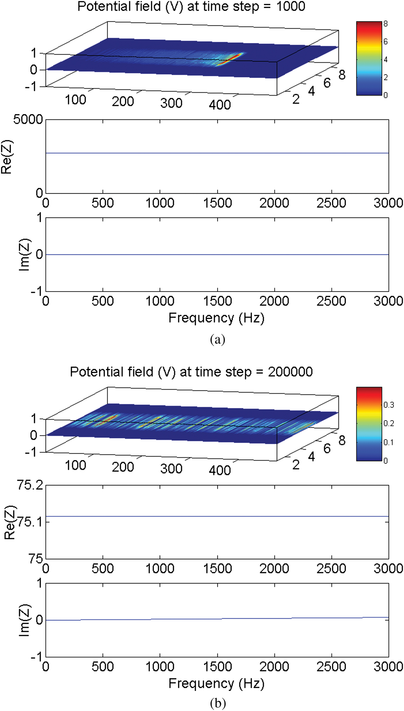
On the other hand, the simulation demonstrates that irrespective of the value of the load impedance, when the transmission line reaches the steady state, the matching condition is always achieved, i.e., the input impedance equals the load impedance (Fig. 2). This is because of the very short electric length of the internodal space in which the frequency and the physical length have both small values. The electric length is given by

Fig. 2. The electromagnetically simulated input impedance of a thin-film microstrip transmission line representing the nerve axon. (a) Input impedance at 1000 timesteps  $Z_{in}=2715.953\; {\rm \Omega }$ (before reaching the steady state). (b) Input impedance at 200 000 timesteps
  $Z_{in}=75.116\; {\rm \Omega }$ (when the steady state has been reached).
 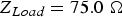 $Z_{Load}=75.0\; {\rm \Omega }$.
 $$\theta=\beta l$$
where 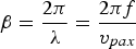 $\beta=\displaystyle{{2\pi } \over \lambda }=\displaystyle{{2\pi f} \over {v_{pax} }}$ is the phase constant, λ is the wavelength, f is the frequency, v pax is the axon impulse propagation velocity (the action potential conduction velocity), and l is the internodal length.
The techniques to analyze and simulate the thin-film microstrip representing internodal space are all described in [Reference Dueñas Jiménez11]. Although the thin-film microstrip is indeed a miniaturized traditional microstrip line located on the top of a carrier substrate, its ground metallization shields the line from the substrate effects and hence a typical microstrip simulation can be performed provided the model parameters of [Reference Schnieder and Heinrich8] are used.
The coincidences between the axon biological model given in [Reference Ferrero Corral, Ferrero y de Loma-Osorio, Saiz Rodríguez and Arnau Vives5], and those of the axon thin-film microstrip model given here, are worth noting. Two parameters showing these concurrences are the conductance and the characteristic impedance.
The conductance of the biological axon can be calculated by means of [Reference Plonsey and Barr6]
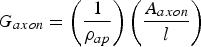 $$G_{axon}=\left({\displaystyle{1 \over {\rho _{ap} }}} \right)\left({\displaystyle{{A_{axon} } \over l}} \right)$$
where A axon is the transverse or cross-sectional area to the direction of the current (the axoplasm area) and ρ ap is the resistivity of the axoplasm.
Similarly, the conductance of the thin-film microstrip axon can be calculated from
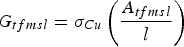 $$G_{tfmsl}=\sigma _{Cu} \left({\displaystyle{{A_{tfmsl} } \over l}} \right)$$
where A tfmsl is the cross-sectional area of the thin-film conductor, i.e., the product of the width of the strip (which is taken equal to the axon inner diameter) by the thickness of metallization and σ Cu is the conductivity of copper.
For a circular biological axon, with a diameter of D axon = 6.2 μm, axoplasm conductivity of σ ap = 0.909 S/m (resistivity of 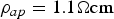 $\rho _{ap}=1.1 \Omega {\rm cm}$) and internodal length of l = 1 mm [Reference Villapecellín-Cid, Roa and Reina-Tosina12, Reference Villapecellín-Cid, Roa and Reina-Tosina13], the conductance will be of G axon = 2.744e − 8 Siemens.
For a planar thin-film microstrip axon, with a strip width of W strip = 6.2 μm, metallization thickness of t = 6.62e − 8 μm, copper conductivity of σ Cu = 5.813e7 S/m, and internodal length of l = 1 mm, the conductance will be of G tfmsl = 2.386e − 8 Siemens.
It is advisable to mention that this extremely thin metallization (only one order of magnitude greater than the classical electron radius, 2.818e − 15 m) is not an actual metallization thickness but its value still remains within the range of validity of the thin-film microstrip model [Reference Schnieder and Heinrich8].
In any case, the agreement between the biological conductance and the thin-film microstrip conductance is certainly notable since the values are in the order of the nS.
The characteristic impedance of the biological axon can be calculated by means of [Reference Ferrero Corral, Ferrero y de Loma-Osorio, Saiz Rodríguez and Arnau Vives5]
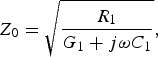 $$Z_0=\sqrt {\displaystyle{{R_1 } \over {G_1+j\omega C_1 }}}\comma \; $$
where
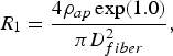 $$R_1=\displaystyle{{4\rho _{ap} \exp \lpar 1.0\rpar } \over {\pi D_{fiber}^2 }}\comma \; $$
 $$G_1=\displaystyle{{4\pi \delta _m } \over {\alpha _m }}\comma \; $$
 $$C_1=4\pi \delta _m C_{am}\comma \; $$
ω = 2πf is the radian frequency, D fiber is the fiber diameter, δ m is the membrane thickness, α m is the membrane surface-resistance product at the internodal space, and C am is the membrane capacitance per unit surface at the internodal space. The inductance per unit length (L 1) has been disregarded because of its small value at the frequency band of interest [Reference Ferrero Corral, Ferrero y de Loma-Osorio, Saiz Rodríguez and Arnau Vives5].
The characteristic impedance of the thin-film microstrip axon can be calculated from the Schneider–Heinrich model [Reference Schnieder and Heinrich8].
Figure 3 shows the characteristic impedance for the aforementioned circular biological [Reference Ferrero Corral, Ferrero y de Loma-Osorio, Saiz Rodríguez and Arnau Vives5, Reference Villapecellín-Cid, Roa and Reina-Tosina13] and planar thin-film microstrip axons in a bandwidth covering from 0 to 20 000 Hz. A perfect agreement between the biological and the thin-film microstrip characteristic impedances (real and imaginary parts) is found throughout the entire bandwidth. A reasonably good agreement is found in all three traces of the impedance modulus at frequencies larger than 10 kHz.

Fig. 3. The characteristic impedance of the circular biological and planar thin-film microstrip axons. Biological (green-square trace) [5]. Thin-film microstrip (red-circle trace). The correspondence is excellent along the bandwidth of interest. Biological (blue-triangle trace) [13].
The other parameter showing a good concurrence between the biological and the thin-film microstrip models is that of a propagation velocity. The propagation velocity of the biological axon can be calculated by means of [Reference Ferrero Corral, Ferrero y de Loma-Osorio, Saiz Rodríguez and Arnau Vives5]
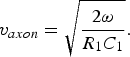 $$v_{axon}=\sqrt {\displaystyle{{2\omega } \over {R_1 C_1 }}} .$$
As mentioned in [Reference Plonsey and Barr6] the propagation velocity depends on the species, the axon diameter, the temperature, etc., but often the membrane resistivity is constant in any one nerve bundle, and a compensatory thermal acclimation maintains a constant relationship between conduction velocity and temperature [Reference Rosenthal and Bezanilla14], then the propagation velocity ties more to fiber diameter. The conduction velocity applies to electric currents on conductors and the propagation velocity to wave propagation on dielectrics.
The propagation velocity (phase velocity) of the thin-film microstrip axon can be calculated from [Reference Dueñas Jiménez11]
 $$v_{tfmsl}=\displaystyle{\omega \over \beta }.$$
Either (8) or (9) can be used as the v pax for the electric length in (1). The curves generated with these equations have a similar behavior (Fig. 4), although a drift going from 1.351 to 19.102 m/s is found for the bandwidth of 20 kHz.

Fig. 4. The propagation velocity of the circular biological and planar thin-film microstrip axons. Biological (green-square trace). Thin-film microstrip (red-circle trace).
III. THE NODE OF RANVIER
In 1952, Hodgkin and Huxley [Reference Hodgkin and Huxley1] presented a model of the nerve axon as a transmission line or cable (the H–H model). Almost a decade later, in 1961, FitzHugh [Reference FitzHugh2] obtained a generalized equation for the relaxation oscillator of Van der Pol (B. Van der Pol designed the oscillator for the Philips Company by using vacuum tubes [Reference Van der Pol15]) to produce a model with a pair of non-linear differential equations. The resulting model named the “Bonhoeffer–van der Pol model” (BVP model) resembled Bonhoeffer's theoretical model for the iron wire model of nerve [Reference Bonhoeffer16]. The BVP model is a simple representation of a class of excitable–oscillatory systems such as the one represented by the H–H model, thereby there is a relationship between the two models manifested in similar physiological state diagrams. The next year, in 1962, Nagumo et al. [Reference Nagumo, Arimoto and Yoshizawa3] made an electronic simulator of the BVP model by using a tunnel diode (Fig. 5).

Fig. 5. Tunnel diode electronic simulator of the BVP model [3].
By cascading the two-port network of Fig. 5 through interstage coupling resistances, Nagumo et al. obtained the active transmission line shown in Fig. 6.

Fig. 6. Active transmission line simulating the nerve axon [3].
In this context, it will be reasonable to consider that the transfer function of Nagumo's active transmission line section can be directly equated to the transfer function of the internodal space, cascaded with the node of Ranvier (i.e., the distributed element transmission line, cascaded with the lumped element active complex load, given by the variable impedance of a tunnel diode), since the former, represented by the BVP model, is very similar to the latter, represented by the H–H model.
Now, the tunnel diode of Figs 5 and 6 can be replaced by a voltage-controlled current source I d (the diode current), by using a modified polynomial representation of its current–voltage characteristics given by the sum of three current components, the tunneling current I t, the excess current I x, and the thermal current I th, which is expressed as [Reference Sze17, Reference Hirasuna and Busdeicker18]
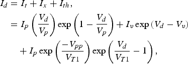 $$\eqalign{I_d& =I_t+I_x+I_{th}\comma \; \cr& =I_p \left({\displaystyle{{V_d } \over {V_p }}} \right)\exp \left({1 - \displaystyle{{V_d } \over {V_p }}} \right)+I_v \exp \left({V_d - V_v } \right)\cr & \quad+I_p \exp \left({\displaystyle{{ - V_{pp} } \over {V_{T1} }}} \right)\exp \left({\displaystyle{{V_d } \over {V_{T1} }} - 1} \right)\comma \; } $$
where V d is the diode voltage, V p = 50 mV and I p = 4.2 mA are the peak voltage and current, V v = 370 mV and I v = 370 μA are the valley voltage and current, V pp = 525 mV is the projected peak voltage, and V T1 = 0.26 mV is the thermal voltage at room temperature, as in [Reference Hirasuna and Busdeicker18].
In this way, Nagumo's active transmission line section, with frequency domain elements, can be arranged as the network of Fig. 7, since the voltage controlled current source is shunt connected. Thus, by shunting the three branches and applying voltage division, the network transfer function can be expressed as follows:

Fig. 7. Nagumo's active transmission line section with frequency domain elements ( $V_d=V_{out} - E_0 {\rm\comma \; }Z_d=V_d /I_d $). (a) A model with a voltage-controlled current source and a membrane resting potential (E 0). (b) A model with a variable impedance and a parametric resistance (R 0).
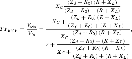 $$TF_{BVP}=\displaystyle{{V_{out} } \over {V_{in} }}=\displaystyle{{\displaystyle{{X_C \displaystyle{{\left({Z_d+R_0 } \right)\left({R+X_L } \right)} \over {\left({Z_d+R_0 } \right)+\left({R+X_L } \right)}}} \over {X_C+\displaystyle{{\left({Z_d+R_0 } \right)\left({R+X_L } \right)} \over {\left({Z_d+R_0 } \right)+\left({R+X_L } \right)}}}}} \over {r+\displaystyle{{X_C \displaystyle{{\left({Z_d+R_0 } \right)\left({R+X_L } \right)} \over {\left({Z_d+R_0 } \right)+\left({R+X_L } \right)}}} \over {X_C+\displaystyle{{\left({Z_d+R_0 } \right)\left({R+X_L } \right)} \over {\left({Z_d+R_0 } \right)+\left({R+X_L } \right)}}}}}}\comma \; $$
where Z d is the diode variable impedance, R 0 is the parametric resistance of the dc source representing the membrane resting potential (E 0),  $X_C=1/\omega C$, X L = ωL, and r = 500 Ω, C = 0.01 μF, L = 4 mH, R = 70 Ω, are the elements used in one of the experiments presented in [Reference Nagumo, Arimoto and Yoshizawa3].
Correspondingly, the transfer function of the distributed element transmission line, cascaded with the lumped element active complex load can be written as [Reference Ferrero Corral, Saiz and Ferrero4, Reference Ferrero Corral, Ferrero y de Loma-Osorio, Saiz Rodríguez and Arnau Vives5]
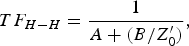 $$TF_{H - H}=\displaystyle{1 \over {A+\lpar B/Z_0^{\prime} \rpar }}\comma \; $$
where
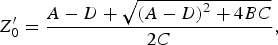 $$Z_0^{\prime}=\displaystyle{{A - D+\sqrt {\left({A - D} \right)^2+4BC} } \over {2C}}\comma \; $$
 $$A={\rm cosh}\left({\gamma l} \right)+Z_0 Y_n {\rm sinh}\left({\gamma l} \right)\comma \; $$
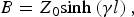 $$B=Z_0 {\rm sinh}\left({\gamma l} \right)\comma \; $$
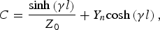 $$C=\displaystyle{{{\rm sinh}\left({\gamma l} \right)} \over {Z_0 }}+Y_n {\rm cosh}\left({\gamma l} \right)\comma \; $$
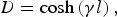 $$D={\rm cosh}\left({\gamma l} \right)\comma \; $$
which become from the matrix product given by
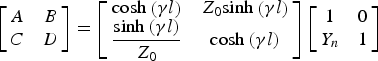 $$\left[{\matrix{ A & B \cr C & D \cr } } \right]=\left[{\matrix{ {{\rm cosh}\left({\gamma l} \right)} & {Z_0 {\rm sinh}\left({\gamma l} \right)} \cr {\displaystyle{{{\rm sinh}\left({\gamma l} \right)} \over {Z_0 }}} & {{\rm cosh}\left({\gamma l} \right)} \cr } } \right]\left[{\matrix{ 1 & 0 \cr {Y_n } & 1 \cr } } \right]$$
and where
 $$Y_n=G_n+j\omega C_n=\displaystyle{\pi \over {\sqrt {\exp \lpar 1\rpar } }}\displaystyle{{D_{fiber} l_n } \over {\alpha _m }}+\displaystyle{\pi \over {\sqrt {\exp \lpar 1\rpar } }}D_{fiber} l_n C_{nm}\comma \; $$
l n is the node length, and C nm is the membrane capacitance per unit surface at the node.  $Z_0^{\prime} $ is the iterative impedance corresponding to infinite sections of the internodal space cascaded with the node of Ranvier [Reference Ferrero Corral, Saiz and Ferrero4] and Z 0 is the characteristic impedance of the distributed element transmission line.
In (18), the first factor corresponds to the chain or [ABCD] matrix of a lossy transmission line (the internodal space), whereas the second corresponds to the [ABCD] matrix of a lumped element active complex load given by the variable impedance of a tunnel diode and represented by a nodal admittance (the node of Ranvier).
Thus, by equating (11) with (12), the diode variable impedance Z d can be obtained in terms of the elements used in one of Nagumo's experiments as will be expressed in the next section.
IV. THE DIODE VARIABLE IMPEDANCE
Since the internodal space is physically a lossy and dispersive (non distortionless) transmission line, the node of Ranvier should effectuate a balancing function to compensate for the losses and eliminate the distortion. In order to do a good description of this function, the tunnel diode representing the node of Ranvier will be better modeled by its variable impedance rather than a voltage controlled current source. The diode variable impedance Z d in terms of a parametric R 0 resistance and depending on the frequency, can be expressed as
 $$Z_d={{\matrix{TF_{H - H} ({R_0 \omega ^2+2175e2R_0 \omega+28.5e9R_0 +100e6\omega} \cr +\,1750e9)- R_0 \left({200e3\omega+3500e6} \right)}} \over {TF_{H - H} \left({\omega ^2+2175e2\omega+28.5e9} \right)- 200e3\omega - 3500e6}}.$$
The inverse discrete Fourier transform of this equation (a continuous non-periodic function suffering from the Gibbs phenomenon [Reference Huybrechs19]) can be used to obtain a direct value of the time-domain load impedance, which should be useful for comparison purposes when diode loaded microstrip interconnects simulations, by means of a convolution procedure [Reference Cárdenas and Jiménez20] or through a two-dimensional finite-difference time-domain method, are performed.
As an active device, the tunnel diode can oscillate spontaneously [Reference Nagumo, Arimoto and Yoshizawa3] and compensate for the losses generated in the thin-film microstrip transmission line (the internodal space). Unfortunately, in the case of distortion, instead of reducing it, the diode contributes to augmenting it, since this active device generates noise and hence distortion. One important contribution to diode noise is thermal noise [Reference Sze17].
The other form to attempt a reduction of the distortion is avoiding it in the thin-film microstrip transmission line representing internodal space. This can be done by way of the well-known Oliver Heaviside's distortionless line theory [Reference Pozar21]. To do this, series compensation inductances (L C), periodically spaced through the entire active transmission line (the entire nerve axon), have to be inserted in order to compensate for the capacitive effect of the line. This procedure, however, also increases the losses. In any case, the final objective is to obtain a constant propagation velocity by generating an inverse function that compensates for the curves of Fig. 4 so as to attain flat traces.
V. CONCLUSION
A thin-film microstrip model to describe the nerve axon has been presented. The circuit analysis demonstrated that the transmission line input impedance tends to the load impedance, whereas the electromagnetic simulation confirmed that, because of the very short electric length of internodal space, the transmission line matching condition in the permanent regime is achieved every time. The correspondence between the calculated characteristic impedances for the circular biological axon, and for the planar thin-film microstrip axon, is very good. Also, the curve behavior for propagation velocity is very similar to both, the biological and the thin-film microstrip axons. In addition, a frequency-dependent function representing the variable diode impedance, has been generated so as to be used instead of the voltage controlled current source, in the analysis and simulation of high-speed interconnects where the pursuit of low distortion and losses is of major importance to improve signal integrity.
ACKNOWLEDGEMENTS
The first author was supported by PROMEP-SEP, México, under grant PROMEP/103.5/11/6834, IDCA 5197, UDG-CA-424. The authors also acknowledge and sincerely appreciate the information and the executable program for synthesizing thin-film microstrips, provided by Professors Dr.-Ing. Frank Schneider and Dr.-Ing. Wolfgang Heinrich.
 Alejandro Dueñas Jiménez was born in Mixtlán, Jalisco, México, on May 11, 1957. He received B.Sc. degree in electronics and communications engineering from the Universidad de Guadalajara, Guadalajara, Jalisco, in 1979 and M.Sc. and D.Sc. degrees in telecommunications and electronics from the Centro de Investigación Científica y de Ecuación Superior de Ensenada, Ensenada, Baja California, México, in 1984 and 1993, respectively. From 1984 to 1994, he was a Professor with the Centro Universitario de Ciencias Básicas de la Universidad de Colima, Colima, México. In 1989, he was a Visiting Assistant Researcher with the LEMA, Département d'Electricité, École Politechnique Fédérale de Lausanne, Lausanne, Vaud, Switzerland. From 2001 to 2002, he was a Guest Researcher with the National Institute of Standards and Technology, Department of Commerce, Boulder, CO., U S A. He is currently a Professor with the Departamento de Electrónica, Universidad de Guadalajara. His research interests include microwave network analysis and synthesis, high-frequency instrumentation and measurement, and mathematical modeling for microwave teaching.
 Ricardo Magallanes Gómez was born in Guadalajara, Jalisco, México, on March 8, 1976. He received B.Sc. degree in electronic and communications engineering from the Universidad de Guadalajara, Guadalajara, Jalisco, Mexico, in 1998. From 1998 to 2008 he worked in the industry on engineering department roles. He is currently pursuing Master's degree from Centro Universitario de Ciencias Exactas e Ingenierias. Since 2009, he has been a Professor at the Instituto Tecnológico Superior de Tala, Tala, Jalisco, México and since 2011 he has also been a Professor on the Mechatronics area at the Centro Universitario de los Valles, Ameca, Jalisco, México. He is presently a Professor in the Departamento de Electrónica, Universidad de Guadalajara, Guadalajara, Jalisco, México. His professional interests include microwave network analysis and synthesis, electronic automation, and mathematical modeling for microwave teaching.
 Judith Marcela Dueñas Jiménez was born in Guadalajara, Jalisco, México on December 31, 1961. She received B.Sc. degree in chemistry from the University of Guadalajara, Guadalajara, Jalisco, in 1980 and M.Sc. in Cellular Biology from the University of Guadalajara, Guadalajara, Jalisco in 1985. In 1995, she obtained Ph.D. degree in Neurobiology and Cellular Biology from University Complutense, Madrid, Spain. In 2006, she was in Santiago-Ramon y Cajal Institute, Madrid, Spain in a sabbatical stay. She is currently a researcher professor at University of Guadalajara. Her research interests include cancer and the effect of estrogens in the differentiation of stem cells. She has been a member of the Society for Neuroscience of E.U.A. since 1996.
 Sergio Horacio Dueñas Jiménez was born in Tenamaxtlán, Jalisco, México on October 16, 1950. He received MD from the Universidad Nacional Autónoma de México in 1975 and the M.Sc. and Ph.D. in Neuroscience from the Centro de Investigación y Estudios Avanzados del Instituto Politécnico Nacional in 1979 and 1983, respectively. From 1986 to 1992 he was a professor in the Centro de Investigaciones Biomédicas de la Universidad de Colima. In 1993, he was in a sabbatical year in the Laboratory of Pablo Rudomin In CINVESTAV del IPN, México. From 1994 to date he has been a full professor in the Centro Universitario de Ciencias de la Salud de la Universidad de Guadalajara. In 1995, he was a visiting professor in the Laboratory of Luis Miguel Segura en el Instituto Cajal, Madrid España. In 2002, he was in a sabbatical year in the Laboratory of Dr R. Burke, NIH Bethesda, Maryland. His research interests include spinal cord neuronal regeneration and control motor.