I. INTRODUCTION
In recent years, the demand for high-speed and high data-rate wireless communication has been increasing gradually. Wideband and ultra-wideband (UWB) low-noise amplifiers (LNAs) have been an area of research interest for many years. In order to achieve high-speed data transmission, LNAs have to meet stringent requirements of gain, bandwidth (BW), noise, and dynamic range. The UWB system is a new wireless technology capable of transmitting data over a wide spectrum of frequency bands with very low-power and high data rates. Although the UWB standard has not been completely defined, most of the proposed applications allow transmission of signals between 3.1 and 10.6 GHz.
Recently, several wideband amplifiers have been demonstrated for either UWB or optical communication applications. In [Reference Ismail and Abidi1, Reference Bevilacqua and Niknejad2], the wideband performances are achieved by using multi-order matching networks; therefore, large chip sizes are unavoidable. Wideband and low-power amplifiers using feedback topologies are popular and have been recently reported in papers [Reference Ellinger, Barras, Schmatz and Jackel3–Reference Bevilacqua, Sandner, Gerosa and Neviani8]. Some of these papers emphasized the low-power consumption for UWB application [Reference Ellinger, Barras, Schmatz and Jackel3–Reference Park, Lee, Cressler, Laskar and Joseph6]. A modified low-power distributed amplifier with programmable-gain control is proposed in [Reference Zhang and Kinget7]. The differential topology of CMOS LNA for 3–5 GHz wideband application is addressed in [Reference Bevilacqua, Sandner, Gerosa and Neviani8].
In this work, we propose a wideband low-power and LNA based on dual resistive-feedback topology. The first stage is the adopted inverter stage with inductive peaking technique for input matching. The second stage, an RC feedback buffer with peaking inductor load is coupled with resistive feedback to drive the 50 Ω output load. The circuit design is discussed in Section 2. We also discuss that the process of the choice with peaking inductor plays an important role on the circuit design. The measurements and simulation results of the low-power LNA are shown in Section 3. Finally, the conclusion is in Section 4.
II. CIRCUIT DESIGN
A) Resistive-feedback inverter for input matching
Figure 1(a) shows the conventional resistive-feedback inverter gain cell without inductive peaking. The BW of the conventional feedback inverter is dominated by the time constant at the input/output node [Reference Chao, Kuo, Lin, Tsai and Wang9]. Therefore, the operating BW will be limited by the parasitic capacitors of the CMOS transistors. Figure 1(b) shows the inverter cell with inductive peaking. The peaking inductor is used to extend the 3 dB BW of the inverter stage. However, since the peaking inductor is loaded at the gate terminals of the NMOS and PMOS of the inverter stage, the peaking inductor is loaded by the gate–source capacitors (C gsn and C gsp) from the gates of both the NMOS and PMOS. If we neglect the small feedback capacitor C gd between the gate and drain terminals, the transfer function of Fig. 1(b) can be derived as [Reference Chao, Kuo, Lin, Tsai and Wang9]:
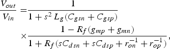 $$\eqalign{\displaystyle{{V_{out} } \over {V_{in} }}=& \displaystyle{1 \over {1+s^2\, L_g \lpar C_{gsn}+C_{gsp} \rpar }} \cr \times & \displaystyle{{1 - R_f \lpar g_{mp}+g_{mn} \rpar } \over {{\rm 1}+R_f \lpar sC_{dsn}+sC_{dsp}+r_{on}^{ - 1}+r_{op}^{ - 1} \rpar }}\comma \; }$$
where g mn and g mp are the transconductance of the NMOS and PMOS, respectively. The C dsn and C dsp are the capacitors between the drain and source terminals, and here r on and r op are the output resistance of the NMOS and PMOS, respectively.

Fig. 1. Single stage of resistive-feedback inverter. (a) Conventional one without inductive peaking. (b) Inverter stage with inductive peaking technique.
From equation (1), resultant poles from the conventional inductive peaking inverter cell and the proposed inductive splitting-load peaking inverter cell are  $\lpar \sqrt {\lpar L_g \lpar C_{gsn}+C_{gsp}\rpar }\rpar ^{ - 1}$. It can be observed that the location of the pole in the proposed structure is boosted to a higher frequency. To investigate the frequency responses of the circuit structures of Fig. 1, their simulated gain performances are plotted in Fig. 2. It is noted that the bias voltage and the device size are the same in the simulations. Compared with the conventional structures in Fig. 1(a), the proposed structure can effectively extend the 3 dB BW to a higher frequency without additional power consumption. It is noted that the peaking inductors in Fig. 1 are all EM-simulated rather than ideal inductors, in order to include all the parasitic effects.

Fig. 2. Simulated gain performances of single-stage inverters according to Fig. 1.
B) Second-stage resistive-feedback amplifier
The basic idea for a circuit of a resistance-feedback wideband amplifier using peaking inductor L in the series with M 1 on the second input stage is shown in Fig. 3(a). The high-frequency simplified model depicted in Fig. 3(b) can be studied and analyzed, and R g is the equivalent gate resistance. In the circuit, M 1, Z L and Z F are the transistor, load, and feedback impedance, respectively. According to Miller's theorem, we can determine that the equivalent input impedance is  $Z_{f1}={{Z_F } / {1+\left\vert {A_v } \right\vert }}$, and the output impedance is
  $Z_{f2}={{Z_F } / {1+\left\vert {\displaystyle{1 \over {A_v }}} \right\vert }}$. We assume that the circuit is connected to a source generator whose impedance R s is typically 50 Ω. In the first approximation, we can derive the analytic expressions of the input impedance (Z inf), noise figure (NF), and gain (|A v|) as the following equations [Reference Chen and Huang10]:
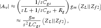 $$\eqalign {\left\vert {A_v } \right\vert & \approx \left({\displaystyle{{1/sC_{gs} } \over {sL+1/sC_{gs}+R_g }}} \right)g_m \left({Z_L \vert \vert Z_{f2} } \right)\cr & \quad \approx \displaystyle{{g_m } \over {s^2 LC_{gs} }}\left({Z_L \vert \vert Z_{f2} } \right)\comma \; }$$
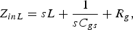 $$Z_{inL}=sL+\displaystyle{1 \over {sC_{gs} }}+R_g\comma \;$$
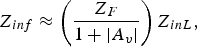 $$Z_{inf} \approx \left({\displaystyle{{Z_F } \over {1+\left\vert {A_v } \right\vert }}} \right)Z_{inL}\comma \;$$
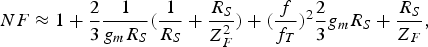 $$NF \approx 1+\displaystyle{2 \over 3}\displaystyle{1 \over {g_m R_S }}\lpar \displaystyle{1 \over {R_S }}+\displaystyle{{R_S } \over {Z_F ^2 }}\rpar +\lpar \displaystyle{f \over {f_T }}\rpar ^2 \displaystyle{2 \over 3}g_m R_S+\displaystyle{{R_S } \over {Z_F }}\comma \;$$
where f T is the transition frequency of the MOSFET. The NF of the first stage is minor when compared to the second stage and it can be ignored by the way of balance circuit. The first reason is the function of the first stage of the circuit is adopted to extend 3 dB BW. The second is because of the input matching. The noise of low-frequency band is strictly depressed by the forward gain. Therefore, the contribution on noise is smaller than in the second-stage amplifier.

Fig. 3. (a) Proposed topology of a resistive feedback with peaking inductor L. (b) Simplified model of a resistive feedback with peaking inductor L.
In order to achieve a trade-off between gain and input impedance matching, the device size can be tuned and determined properly in the design process. From equations (2) and (4), the inductor results in a slight decrease of the gain. If the inductance is properly chosen, it can affect the 3 dB BW extension. Owing to the input impedance of the transistor, it can be viewed as capacitive, and it will be the RC filter function to form the narrowband response. Therefore, if the peaking inductor is accurately chosen and inserted into the input node of the circuit, the frequency response of the BW can be expanded. This is the reason why we use the peaking inductor in the circuit. The leading phase of the inductor can be balanced with the lagging phase of the capacitor.
Dealing with NF and BW, it was found that high A v and small Z F lead to a wider −3 dB BW. However, due to the NF degradation, a smaller Z F is not a desirable approach in equation (5). Therefore, high-voltage gain (A v) or large transconductance gm (compatible with “term is magnified by gm”) is a better choice to increase the BW and also lower the NF. Nevertheless, in CMOS technology, because of poor transconductance, higher A v requires a dramatically larger and prohibitive DC current. All the internal noise sources of the amplifier can be represented by the input referred shunt noise current and series noise voltage sources in a two-port noise model. The detailed analysis can be referenced in [Reference Chen and Huang10]. However, the feedback resistance is usually pretty large so that the added noise to the amplifier is limited; moreover, the R f term is magnified by g mReference Bevilacqua and Niknejad2. The large value of R f will also result in a little deviation of the G opt of the amplifier from the value without feedback. This characteristic can be observed from Fig. 4. G opt is the optimum conductance at the condition of the optimum value of source admittance for minimum NF.

Fig. 4. Source impedances of the common-source CMOS amplifier for maximal gain (Γmax) and optimal NF (Γopt) from 1 to 10 GHz: (a) without shunt feedback and (b) with shunt feedback.
The purpose of LNA input matching design is to enhance the gain and minimize the NF. However, the input matching conditions for maximal gain and minimal NFs are usually different. For CMOS amplifiers, the optimal noise input that matches admittances with and without shunt feedback will not vary much if g m2R f is quite large. On the other hand, the shunt feedback provides a way to manipulate the amplifier input impedance. Figure 4(a) shows the maximal gain input matching reflection coefficient (Γmax) and optimal noise input matching refection coefficient (Γopt) of the common-source amplifier without feedback from 1 to 10 GHz. After adding the shunt feedback, the Γopt of the amplifier is barely moved, and the Γmax is shifted toward the Γopt as shown in Fig. 4(b). Hence, a better design trade-off between the gain and NF of the broad-band CMOS LNA can be obtained. In other words, there is larger deviation for both Γopt and Γmax without a shunt feedback loop. If the shunt loop is added into the circuit, then the locus of Γopt and Γmax can be achieved simultaneously.
C) The proposed topology
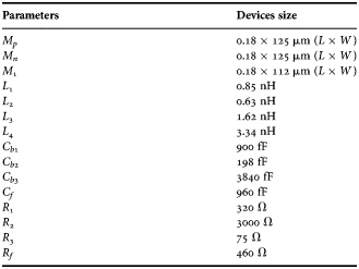
The proposed low-power and LNA is shown in Fig. 5, which consists of the input matching network that is implemented by a resistive-feedback inverter. The resistive-feedback inverter consists of M p, M n, and R 1; the output stage is the resistive-feedback amplifier, which consists of M 1, L 2, L 3, L 4, R 2, R f, and C f. Although, R 3 and L 4 can control the gain behavior at the low band, the gain control at the high band is determined by M 1 and feedback loops R f/C f and L 3. The inductors L 1, L 2, and L 3 can provide the function of the inductive peaking.

Fig. 5. Schematic representation of the proposed resistive-feedback LNA.
Figures 6(a) and 6(b) show the peaking effect with different inductor values. Generally speaking, the property of the input impedance of the transistor can be viewed as capacitive. When the signals go through the transistor, the 3 dB BW will degrade with the capacitive effect. If the inductor is properly chosen and adopted in the circuit, then the 3 dB BW will be expanded by the peaking effect. This phenomenon is shown in Figs 6(a) and 6(b). Here, we choose the value of the inductors L 2 and L 3 as 0.63 and 1.62 nH, respectively. The resistor R f has equivalent resistance by the Miller theorem to provide 50 Ω matching. C b1, C b2, and C b3 are the block capacitors. The sizes of the circuit devices in the proposed structure are shown in Table 1. The simulations showed that the proposed circuit has a stability factor >2 from 1 to 10.5 GHz.

Fig. 6. (a) L 2 peaking inductor effect. (b) L 3 peaking inductor effect.
Table 1. Circuit device size.

III. MEASUREMENT RESULTS
Figure 7 shows the die photo of the two-stage wideband amplifier, which has a chip size 0.69 mm2. In Fig. 8, it can be seen that the input return loss (S 11) is lower than −8 dB, but in Fig. 9 it can be seen that the output return loss (S 22) is lower than −10.8 dB from 1 to 10 GHz, respectively. In Fig. 10, it can be seen that the NF is located between 4.2 and 5.2 dB in the whole band. The difference between the simulated and measured data below 3 GHz can be ascribed to the oscillating behavior of S 11 (see Fig. 8). The power gain whose peak value is 10.5 dB at 2.4 GHz is shown in Fig. 11. The differences between the simulated and measured gain can be ascribed to the parasitic capacitor of the IC pad, which has to be considered in the design process. Moreover, increasing the value of the inductor L 3 could improve the gain performance. In Fig. 12, the third-order input intercept point (IIP3) at 4.98 and 5.02 GHz is 1 dBm. The power consumption is 12.65 mW at 1.5 V supply voltage.

Fig. 7. Layout of the proposed UWB LNA.

Fig. 8. Simulated and measured results of input return loss (S 11).

Fig. 9. Simulated and measured results of output return loss (S 22).

Fig. 10. Simulated and measured results of NF.

Fig. 11. Simulated and measured results of power gain (S 21).

Fig. 12. Measurement of IIP3.
To compare the overall performance of our LNA with the previously published ones, a figure of merit (FOM) that takes into account the gain, F, BW, area, and the DC power consumption of the LNA is defined as [Reference Hsu and Hsu11, Reference Gramegna and Erratico12].
 $${\rm FOM}_A=\displaystyle{{{\rm Gain}_{max} \, \lpar {\rm dB}\rpar \times {\rm BW}\, \lpar {\rm GHz}\rpar } \over {\lpar F - 1\rpar \times P_{DC} \, \lpar {\rm mW}\rpar \times {\rm Area}\; \lpar {\rm mm}^2 \rpar }}\comma \;$$
where BW is the 3 dB BW with frequency of operation in GHz, P dc is the power consumption in milliwatts, and the values of the gain and noise factor F are their absolute values. Area represents the chip area and its value is respective to a typical area of 1 mm2.
The performance comparison of the proposed circuit with other reported papers is shown in Table 2. Compared with these amplifiers, this work achieves the third highest FOMA and the lower-power consumption. For low-power applications, the performance of our work is compatible to other LNAs. The proposed circuit shows a good performance for wideband and low-power applications.
Table 2. Measurement comparison of the familiar topology LNA with other reported LNA.

IV. CONCLUSION
We have presented a low-power, wideband CMOS LNA with resistive feedback. The proposed resistive-feedback inverter is employed to achieve wideband input matching and save chip area. The power consumption is 12.65 mW with a 1.5 V supply voltage. In the whole band, the maximum power gain is 10.5 dB and the minimum NF is 4.2 dB. Our work shows a good performance for wideband and low-power applications.
ACKNOWLEDGEMENTS
The authors would like to acknowledge the Taiwan semiconductor manufacture company (TSMC) and chip implementation center (CIC) for the wafer fabrications.
 Meng-Ting Hsu was born in Changhua, Taiwan, Republic of China in 1961. He received his B.S. and M.S. degrees from Chung-Yuan Christian University in the Electrical and Electronic Engineering in 1989 and 1991, respectively. Since 1992 he has served as a lecturer in the Electronic Department of the National Yunlin University of Science and Technology (NYUST), and he later obtained a Ph.D. degree from National Chiao-Tung University in Communication Engineering in 2004. In 2005, he was promoted to associate professor and has more than 10 years experience in microwave circuit design. His current research interests are in noise theory application on MMIC and CMOS RFICs.
 Shih-Yu Hsu was born in Pingtung Taiwan, Republic of China in 1980. He received his B.S. degree in electrical engineering from Cheng Shiu University of Science and Technology in 2003. He received an M.S. from the National University of Science and Technology in electrical engineering from 2007. His current research interests are in CMOS RFICs.
 Yu-Hwa Lin was born in Taichung, Taiwan, Republic of China in 1989. He received his B.S. in electrical engineering from Southern Taiwan University of Science and Technology in 2010. Since then, he had been pursuing his M.S. at the National Yunlin University of Science and Technology in electrical engineering. His current research interest is in CMOS RFICs.