I. INTRODUCTION
In the past years, 60 and 120-GHz short-range wireless digital radios have been evolving [Reference Niknejad1, Reference Takahashi, Kosugi, Hirata, Murata and Kukutsu2]. Many implementations of such radios rely on simple modulation formats such as amplitude-shift-keying (ASK) or quadrature-phase-shift-keying (QPSK). In order to realize higher-order modulation formats and improve the spectral efficiency [Reference Lu, Zhang, Funada, Sum and Harada3], a medium resolution digital-to-analog converter (DAC) operating at few Giga-sample-per-second (GS/s) must be incorporated in the transmitter part of radios. Such a DAC can also be used for pulse shaping [Reference Barale, Iyer, Perumana, Sen, Sarkar and Rachamadugu4]. Integrating the DAC with a radiofrequency (RF) frontend circuitry (up conversion mixers and power amplifiers) improves the bandwidth and lowers the power dissipation of the DAC by removing the impact of the parasitics associated with the pad and package. The ultra high-speed RF frontends of such applications can optimally be implemented in a SiGe BiCMOS technology. That means the DAC should be realized in such technologies as well. The SiGe BiCMOS process is an attractive option, because it promises further integration of RF frontend and DAC with CMOS baseband processing logic. This paper focuses on the low-power implementation of a medium resolution DAC in SiGe BiCMOS technology.
In recent years, 6-bit DACs with sampling rates in excess of 20 GS/s have been implemented in SiGe BiCMOS [Reference Khafaji, Gustat, Sedighi, Ellinger and Scheytt5], CMOS [Reference Greshishchev, Pollex, Wang, Besson, Flemeke and Szilagyi6], and InP [Reference Nagatani, Nosaka, Yamanaka, Sano and Murata7] processes. Such converters are not targeted for system-on-chip applications, and at best, offer a power dissipation of 0.75–1 W (see [Reference Khafaji, Gustat, Sedighi, Ellinger and Scheytt5–Reference Nagatani, Nosaka, Yamanaka, Sano and Murata7]). Table 1 lists some examples of DACs operating from 1 to 12 GS/s. The current steering topology is the most used approach for DAC realization at this speed class. The challenge in the design of such DACs is to obtain sufficient spurious free dynamic range (SFDR) at high output frequencies, which is directly related to the output impedance of the switching transistor. While recent multi-GS/s DACs, shown in Table 1, are implemented in CMOS technology, the limited output impedance of advanced CMOS transistors necessitates extra circuitry/techniques such as cascoding [Reference Lin, van der Goes, Westra, Mulder, Lin and Arslan14] or double sampling [Reference Tseng, Wu and Chu10], to obtain a good SFDR at high frequencies. From this perspective, a BiCMOS implementation seems promising, because of the larger output impedance of SiGe hetero-junction bipolar transistor (HBT). For aforementioned wireless systems, power dissipation is another important parameter. Table 1 shows an expected correlation between full-scale output current and power consumption of a DAC. A higher full-scale output current, translates into larger devices in the current switching array, which, in turn, results in a bigger capacitive load for the digital circuitry (driving the current cell array) and higher power consumption. This points to the advantages of full integration; a stand-alone DAC is usually designed to drive low Ohmic (e.g. 50 Ω) loads. Hence, to achieve a practical output voltage swing across such loads, a large peak-to-peak current must be provided by the DAC, increasing the current consumption. Alternatively, if the DAC is monolithically integrated within a system, the load resistance of the DAC can be selected in the few hundreds ohm range, thereby reducing the DAC full-scale current.
Table 1. Examples of high-speed DACs.

In this paper, we design a current steering DAC that can be embedded into a protocol-agile wireless transceiver. We demonstrate the possibility of avoiding segmentation by employing a new topology for the current switch array and taking advantage of high-speed HBTs of a BiCMOS technology. A resolution of 8 bits and a signal bandwidth of 1 GHz are selected. To ease the post-filtering (smoothing filter), the sampling rate of the DAC needs to be 3–5 times larger than the signal bandwidth. A sampling rate of 5 GHz is therefore chosen. The prototype presented in this paper provides small core area (0.06 mm2), low power (26 mW) and high SFDR (48 dB), which makes it an attractive choice for many applications. This paper is organized as follows; in Section II, challenges of the design of a low-power BiCMOS DAC and the proposed solution are described. In Section III, different parameters affecting the circuit performance are studied. Section IV presents the prototype chip and measurement results. Conclusion is drawn in Section V.
II. DAC TOPOLOGY
There are three main approaches to realize a current steering DAC as shown in Fig. 1. All three topologies have similar full-scale output current of I FS. In the N-bit full-binary realization of Fig. 1(a), N differential pairs are used as current switching cells (CSC), and the tail currents are scaled from I FS/2 to I FS/2N. The second approach, shown in Fig. 1(b), uses an R-2R ladder to implement the binary weights [Reference Razavi15], while all CSC have the same tail current. Fig. 1(c) illustrates the third approach, often called segmentation, which uses an M-bit unary section, consisting of 2M−1 similar CSCs and a (N-M)-bit binary section. Segmented architecture requires encoding of M digital inputs from binary into thermometer code. Generally, the outputs of the thermometer decoder have to be retimed with each other and with the binary section as well.

Fig. 1. Three realizations of an N-bit current steering DAC.
Table 2 compares the three topologies in terms of the total current dissipation in the CSC array, and the complexity of the digital circuitry regarding the latches or flip-flops preceding the CSC and also the thermometer decoder (not shown in Fig. 1). As it can be seen, the binary DAC has the least current consumption and complexity. Compared with the binary topology, the R-2R DAC consumes more power in the CSC array, whereas the segmented DAC consumes more power in the digital circuitry. At high sampling rates, the thermometer decoder and retiming flip-flops not only dissipate extra power but also result in larger silicon area. The increased area of the digital block necessitates longer tracks for interconnecting blocks and also for the clock signals, which, in turn, increases the power dissipation of the clock driver circuitry.
Table 2. Comparison of conventional topologies (N: DAC resolution; M: bits for unary part).
One drawback of the binary topology is related to the limited current gain (β) of the bipolar transistor and variation of β with the collector current itself. To obtain the highest accuracy, we should size the switching transistors according to the tail current source. That means the least-significant-bit (LSB) CSC uses the minimum-size transistor, and the MSB switching transistors are 2N−1 times larger. This leads to a very large transistor for the MSB cell, introducing a large capacitance at the input of the cell, the common emitter node of the switching pair, and in addition, at the output node of the DAC. On the other hand, if we do not scale the size of switching transistors, the dependency of β and common-base current gain (α) on the collector current will deteriorate the accuracy. Typically, β of a transistor is maximum at medium collector currents and it decreases when the collector current approaches I C,fTmax (the collector current at which the transit frequency, f T, is maximum), or when collector currents is very low [Reference Gray, Hurst, Lewis and Meyer16]. This means that the ratio between collector and emitter currents of the switching transistors is different for different CSC. Representing the current gain of the switching transistor by β LSB and β MSB for a collector current of I FS/2N and I FS/2, respectively, we will have
Thus, the error in the output current of MSB cell is
For example, for an 8-bit DAC, if β LSB is 50 and β MSB is 200, the error in the MSB current will be 1.92I LSB.
Another drawback of the binary method is related to the different switching speed of CSC. Assuming that a CSC is driven by a current-mode-logic (CML) circuit with a collector resistor of R C and a parasitic output capacitance of C C, the time constant of the circuit can be written as
where r π1, C π1, and C μ1 are small-signal base-emitter resistance, base-emitter capacitance, and base-collector capacitance, respectively. Parameter A is the small-signal voltage gain of the stage and C con is the capacitance of interconnects between the CML driver stage and the switching cell. Capacitor C π1 can be represented as (I C/v T) τ F + C je1, where τ F is the forward transit time of the base charge, v T is the thermal voltage (26 mV at room temperature), and C je is the base-emitter junction capacitance [Reference Gray, Hurst, Lewis and Meyer16]. For a switching transistor that is K times the minimum-size transistor, Equation (3) can be rewritten as
where C je and C μ represent the parasitic capacitances of a minimum-size transistor. Figure 2 illustrates the variation of the time constant versus tail current source in a CSC, calculated using (4). If the driver circuitry is the same for all CSC, it is not possible to obtain similar time constants for different cells in a binary DAC. This will introduce cell-dependent delay difference among cells and deteriorate the SFDR [Reference Chen and Gielen17]. The lower the difference among tail currents, the lower the difference among time constants will be. From (4), one can expect that it is possible to make time constants equal by having dissimilar R C (i.e. different driver output resistance) for each CSC driver. However, this is difficult to guarantee (without some type of calibration) because majority of the parameters in (4) are process dependent. Moreover, R C has a relation with the speed and the output swing of the driver stage and changing R C can result in different time constants in different driver stages.
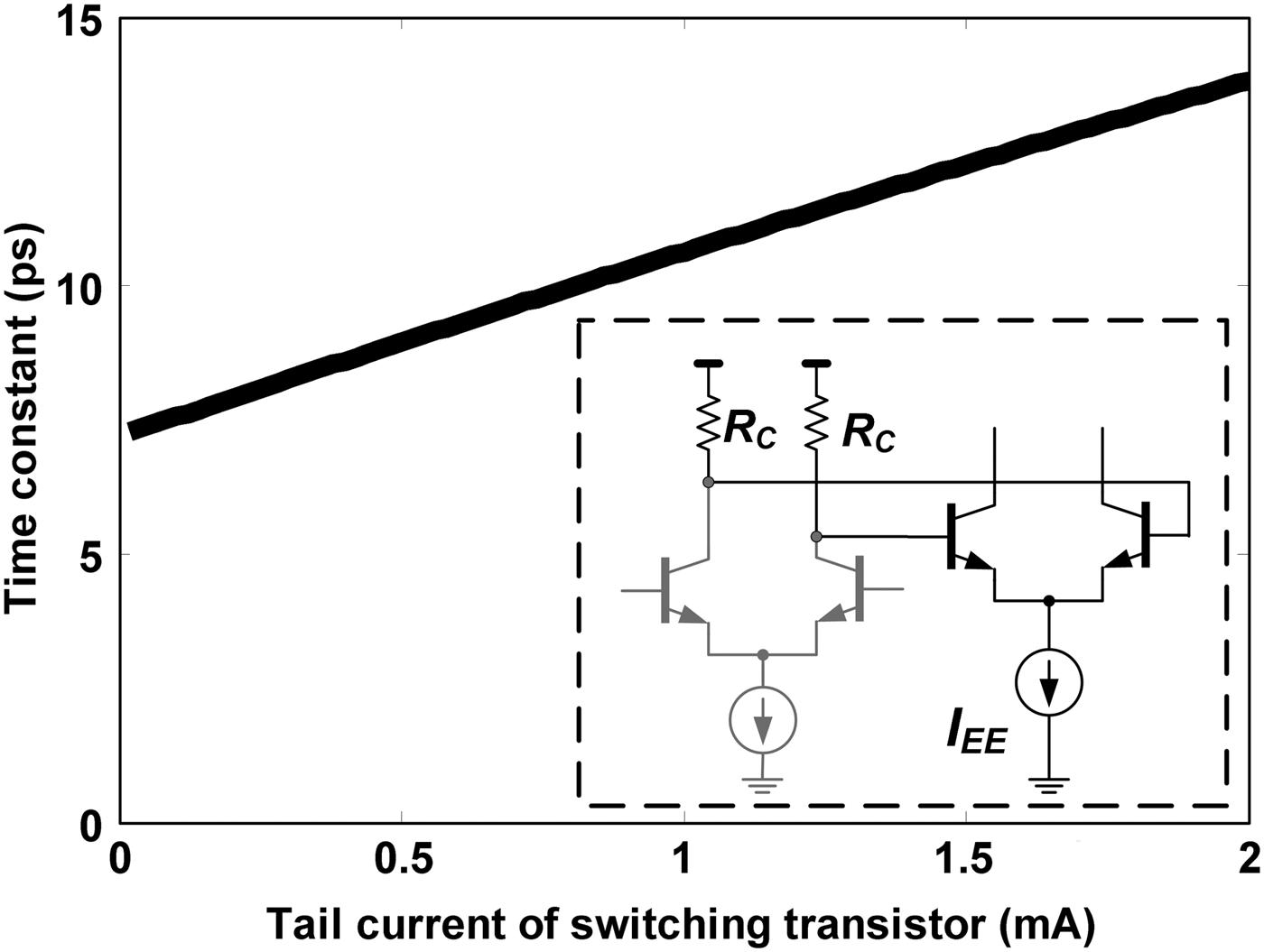
Fig. 2. Variation of the time-constant of a CSC with the tail current (I EE).
Because of the aforementioned drawbacks of full-binary DACs, R-2R, and segmented architectures are often utilized to achieve a good linearity and dynamic performance. Here, we propose a solution based on the idea that minimizing the difference of the tail current sources in a binary DAC can improve the accuracy and dynamic performance. This is done by simultaneous usage of the full-binary structure for the MSB cells and R-2R ladder for the LSB cells. The architecture of the designed 8-bit DAC is shown in Fig. 3. The tail currents of the first two MSB cells are scaled, but for the remaining bits, the current weighting is performed by a resistive R-2R ladder. The advantages of this method are
• Current consumption is equal to 1.5I FS, significantly smaller than that of a complete R-2R implementation shown in Fig. 1(b)
• The number of latches is still N = 8 and there is no need for a thermometer decoder
• The ratio of the currents in the switching cells is only 4, and therefore, the current mismatch of cells and the impact of β variation are small. This results in a lower integral non-linearity (INL) and differential non-linearity (DNL), when compared with that of Fig. 1(a). The reduced ratio of the transistor sizes keeps the parasitic capacitances at the collector node of the tail current transistors small, resulting in high output impedance at high frequencies. The code-dependent delay difference among different bits is also decreased compared with the full-binary circuit of Fig. 1(a), resulting in a better SFDR.

Fig. 3. Proposed binary-weighted DAC.
III. CIRCUIT DESIGN
A) Mismatch
The static accuracy of the DAC is mainly a function of mismatch of emitter resistors (R E, 2R E, and 4R E), transistors of tail current sources, and also the mismatch of the resistors in the ladder (R and 2R). In Fig. 3, the mismatch between two current sources of size I u = I FS/8 can simply be calculated using the method in [Reference Razavi15] as
where ΔV BE is the base-emitter voltage mismatch of two minimum-size transistors, and Δ(4R E) is the mismatch of the 4R E resistors. By choosing a large R EI FS in (5), we can reduce the impact of V BE mismatch.
We can determine the mismatch requirements for obtaining a certain INL (typically 0.5 LSB) using Monte-Carlo simulation. Figure 4 shows the results of a Monte-Carlo simulation. As it can be seen, standard deviation mismatch of 1% for the ladder resistor R and 0.25% for 4R E result in a worst case INL of 0.4 LSB. In this design, the mismatch of the emitter degeneration resistors is more influential than that of the ladder resistors because the R-2R ladder is used for the LSB cells, and the accuracy of the MSB and MSB-1 currents is independent of the ladder. Figure 4(c) shows the result for the case where mismatch of all resistors and transistors is taken into account. Size selection and layout are done carefully in order to provide an INL below 0.5 LSB in 99.7% of cases.

Fig. 4. Monte-Carlo simulation results (1000 runs) for: (a) σ R = 0.01 for the ladder resistance, (b) σ 4RE = 0.0025 for the emitter resistance, and (c) including all mismatches.
B) Output impedance of CSC
The DC output resistance of the CSC affects INL and DNL. As the output frequency increases, the output impedance of the CSC is degraded by parasitic capacitances. This effect can be analyzed according to the method used in [Reference van den Bosch, Borremans, Steyaert and Sansen12, Reference Van den Bosch, Steyaert and Sansen18]. Figure 5 shows the magnitude of the output impedance of the smallest current switch (biased at I FS/8), with and without considering the collector capacitance of the switching transistor. For the cells that are connected to the ladder, the collector capacitances of the switch (C O in Fig. 5) will affect the high-frequency performance of the DAC. For the cells directly connected to the output, these capacitors can be considered as part of the load capacitance (and cannot generate distortion if their voltage dependency is small). The magnitude of the output impedance including collector capacitance (zcsO) at the output frequency of f out (>p 0) is given by
where r o is the collector-emitter resistance of the switch transistor and p o is the frequency at which the output impedance starts to decrease:

Fig. 5. Output impedance of the current switching cell (C CS is the collector-substrate parasitic capacitance, and C 1 is the total parasitic capacitance at the emitter of Q 1 and can be approximated by C π1).
Equation (6) shows that for CSC connected to the ladder, it is important to keep the parasitic output capacitance of the switch transistor to a minimum. That is to use the minimum-size transistor. A formula for the INL caused by the limited output impedance of the CSC connected to an R-2R ladder is numerically found as
where J (≤N) is the number of cells connected to the R-2R ladder. We want the impact of the output resistance on the INL to be much less than the INL caused by mismatch, e.g. INLr < 0.1 LSB. To satisfy this condition, the output impedance should be above 51 kΩ in this design. This is feasible, as shown in Fig. 5, since the output impedance remains above 70 kΩ up to 1 GHz, due to the low parasitic capacitances of the minimum-size bipolar switch transistors.
For the MSB cells that are directly connected to the output node, the magnitude of the output impedance (without C O) at f out is given by
where p 1 is the frequency at which |z cs| starts to decrease:
Equation (9) is valid, if r π1 is much smaller than the output resistance of the tail current source, and if capacitance C 1 is dominated by C π1. To achieve an SFDR of 20 log(1/Q), the output impedance must remain above [Reference Van den Bosch, Steyaert and Sansen18]
in which R L is the load resistance, and is equal to the ladder resistance in this design. Q is the ratio of the largest output harmonic to the fundamental tone. Equation (11) is obtained for a conventional DAC having 2N − 1 identical CSC. For the proposed structure, the formula can be modified by replacing 2N − 1 with the number of unit cells that are directly connected to the output. For example, for the 8-bit DAC of Fig. 3, three CSC, biased at I FS/2, I FS/4, and I FS/8, are connected to the output node. This is equivalent to seven unit cells, each biased at I FS/8, connected to the output. Replacing 2N−1 with 7 in (11), our design requires |z cs| > 0.14 MΩ for an SFDR of 50 dB. This is satisfied, thanks to the large output resistance and the high f T of the HBT switch transistor.
C) Delay difference of CSC
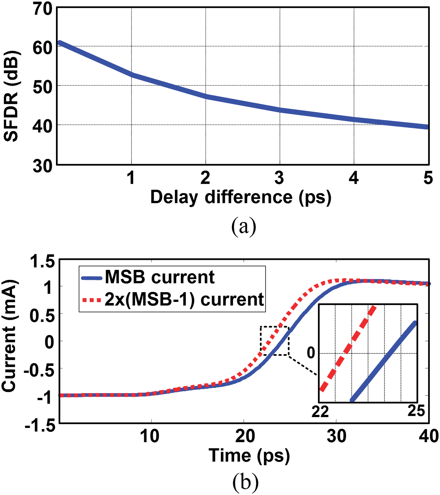
Another source of dynamic performance degradation is the difference in delays of different CSC [Reference Chen and Gielen17]. A system level simulation was performed in which the delay of the CSC of the MSB was changed while other CSCs were assumed to have similar delay. The result of this simulation is shown in Fig. 6(a). Up to a delay difference of 1.5 ps, the SFDR remains above 50 dB. Next, a transistor-level simulation was performed. Figure 6(b) compares the output current of the MSB cell with twice the current of the MSB-1 cell. The cells have different time constants, as predicted by (4), and therefore not only the delay but also the rise time is different. The difference in the time constant of the cells is sufficient for an SFDR better than 50 dB at 1 GHz. Keeping the delays as close as possible also requires careful layout of the clock distribution network and the current summation network at the output of the CSC.

Fig. 6. (a) Impact of the MSB timing skew on SFDR (f out = 1 GHz) and (b) simulated timing skew between I MSB and 2 × I MSB−1 cells.
D) Latch
In this design, we use similar latches at the input of all CSCs. In the latch, shown in Fig. 7, minimum-size bipolar transistors are used to reduce the size and power dissipation. The latch is based on the standard CML family. In addition, transistors Q5 and Q6 are added to reduce the input data feedthrough when the latch is in the “hold” state (i.e. Q1 is off). If the input data feedthrough was not eliminated, we would need to add a limiting amplifier at the output of the latch, to prevent any feedthrough from reaching CSC, and that would increase the power dissipation. As shown in Fig. 7, transistor M2 provides a small current to flow through the cross-coupled latching transistors, and it avoids complete turnoff of this stage when Q2 is off. This results in shorter regeneration time when the latch goes from the track state to the hold state. The capability of setting/resetting is also foreseen for future applications (e.g. calibration).

Fig. 7. The high-speed latch.
IV. MEASUREMENT RESULTS
The DAC is fabricated in a 0.13 µm SiGe BiCMOS process. Figure 8 shows the chip micrograph. The total active area of the DAC (excluding the input buffers) is 0.06 mm2. The size of the die is limited by the number of pads. To avoid using large silicon area for such a small circuit, the input bits are single-ended (as opposed to the conventional differential signaling). On-chip differential pairs are used to convert the single-ended input signals to differential. As explained later, this has a negative impact on the performance of the DAC.

Fig. 8. Chip photograph.
In the measurements, the DAC die was directly wire-bonded to a printed circuit board. Figure 9 shows the results of non-linearity measurements. INL and DNL measurements were performed by applying a low-speed digital ramp to the DAC and measuring the output signal using a high-impedance precision voltmeter. The DNL and INL are below 0.58 and 0.29 LSB, respectively. The peak in the DNL at the mid-range is the well-known characteristic of a binary-weighted DAC. The DAC dissipates 12 mW (from a 3 V supply) in analog section and 14 mW (from 2 V supply) in digital parts. The peak-to-peak differential output current is 4 mA. This output current results in a 1 V pp,diff full-scale output voltage swing, if the load impedance is much larger than the ladder resistance (250 Ω). The full-scale output swing reduces to 0.167 V pp,diff for a 100 Ω differential load.

Fig. 9. Measured static performance of the DAC.
For dynamic measurement, Agilent's 81250 ParBERT was used to generate the data pattern. Clock signal of the DAC was generated by an Agilent E8257 low-jitter signal generator. The differential output of the DAC was converted to single ended (by a passive phase shifter and a power combiner) and then it was applied to Advantest U3772 spectrum analyzer. Due to the limited speed of the pattern generator, the DAC can be fully characterized up to 3.3 GS/s only. To measure the performance of the DAC at 5 GS/s, a 2.5 GS/s pattern was generated but, the clock of the DAC was 5 GHz. Figure 10 shows the SFDR measurements at two different sampling rates. As it can be seen, SFDR remains above 48 dB up to 1 GHz output frequency. The time domain performance was evaluated as well. MSB was changed from 1 to 0 and then the output was captured by an Agilent DCA86100 sampling oscilloscope. A 20–80% rise time of 29 ps was measured. Assuming first-order frequency response, the time constant and bandwidth of the output can be approximated by 21 ps and 7.6 GHz, respectively. The settling time is 110 ps, well below 200 ps which is required for 5 GS/s operation.

Fig. 10. Variation of SFDR with signal frequency.
Figure 11 shows an example of the output spectrum. The SFDR is limited by the second-order harmonic. This is the case for all high-frequency outputs and it can also be reproduced in simulations. The reason of having a large second harmonic in the differential output was carefully investigated. It was found that the even harmonics at the output are generated because of a small variation in the period of the on-chip clock signal. The input clock is a single-ended sine-wave that is converted to a differential square-wave by a differential pair. When the single-ended input bits of the DAC are changed, a small variation in the on-chip digital ground potential happens due to the current in 50 Ω termination resistors. This variation in the ground potential is equivalent to variation of threshold voltage of the single-ended-to-differential converter. Consequently, the clock period is slightly (1–2 ps) changed with the input data pattern, resulting in the output distortion. The degradation of the SFDR at frequencies higher than 1 GHz in Fig. 10 is believed to be caused by this problem. This phenomenon can be alleviated by using a clock input with faster rise/fall times. This is the reason why in Fig. 10, the SFDR improves by increasing the clock frequency. Employing differential signaling for both data and clock inputs could be a better solution. After fixing this problem, and according to both theoretical analysis and transistor-level simulations, we expect the SFDR of the DAC to remain above 48 dB up to the Nyquist output frequency. As shown in Fig. 11, even in the current design, the third harmonic level of the output signal is −55 dB, which shows that the distortion caused by the finite output impedance and data-dependent delay is acceptable for 8-bit operation. Effective number of bits (ENOB) of the DAC, derived from the measured spectrum, is close to 8 bit at low-output frequencies but drops to 6.8 bit when output frequency approaches 1 GHz. Reduction of the ENOB is also contributed to the harmonics and spurs that are caused by the variations of the clock period. Table 3 summarizes the specification of the DAC.

Fig. 11. Output spectrum at f out = 985 MHz, and f CK = 5 GHz: (a) measured and (b) simulated.
Table 3. Measurement summary.

V. CONCLUSION
A high-speed, low-power, binary-weighted DAC was presented. This work shows that modern BiCMOS technologies offer the capability to realize high-performance CSC for a medium-resolution binary-DAC in the GHz range. A prototype chip was fabricated and an SFDR of 48 dB was achieved up to 1 GHz output frequency, while dissipating only 26 mW.
ACKNOWLEDGEMENTS
This work was in part supported by the Celtic project 100GET. Authors would also like to thank Mr Frank Popiela from IHP for preparing the test PCB.
 Behnam Sedighi received the Ph.D. degree from Sharif University of Technology, Tehran, Iran, in 2008. He has been with KavoshCom, Tehran, Iran, as a Senior Designer, and with United Microelectronics Corporation (UMC), Hsinchu, Taiwan, as a Doctoral Intern involved with high-speed analog integrated circuits and data converters. From 2009 to 2011, he was a Senior Research Scientist with IHP Microelectronics, Frankfurt (Oder), Germany, where he was developing analog/mixed-signal circuits for optical communications. He joined center of energy efficient telecommunications, University of Melbourne, VIC, Australia in 2011. He is now with National ICT Australia, University of Melbourne, VIC, Australia. His research interests include data-converters, broadband ICs, and nanoelectronics.
 Mahdi Khafaji was born in Tehran, Iran, in 1982. He received the B.Sc. and M.Sc. degrees in electronic engineering from the University of Tehran, Tehran, Iran, in 2004 and 2007, respectively, and is currently working toward the Ph.D. degree with the Dresden University of Technology (TU Dresden), Dresden, Germany. In 2007, he was with KavoshCom, Tehran, Iran. Since 2008, he has been with IHP Microelectronics, Frankfurt (Oder), Germany. His research interests include high-speed data converters and broadband circuits for optical communication.
 Johann Christoph Scheytt received the Diploma degree (M.Sc.) and Ph.D. degree (with highest honors) from Ruhr-University, Bochum, Germany, in 1996 and 2000, respectively. In 2000, he co-founded advICo Microelectronics GmbH, a German integrated circuit (IC) design house. For 6 years, he was the Chief Executive Officer (CEO) with advICo Microelectronics GmbH, during which time he was responsible for various projects in the area of wireless and fiber-optic IC design. Since 2006, he has been with IHP Microelectronics, Frankfurt (Oder), Germany, where he is Head of the Circuit Design Department, a group of about 30 researchers involved with high-frequency and broadband IC design. He has authored or coauthored over 80 papers. He holds 12 patents. His research interests include RFIC and broadband IC design, phase-locked loop (PLL) techniques, and design with SiGe BiCMOS.