


Introduction
For measuring the impulse response function (IRF) of a device under test (DUT), continuous binary coded excitation signals are often used. One reason is the high signal-to-noise ratio (SNR), because of the large signal energy of the continuous signal. Another reason is the relatively simple and cheap signal generation in digital electronics. An approximation of a delta-impulse shaped autocorrelation function (ACF) of the binary coded excitation signal is needed in order to obtain good results for the IRF. For this purpose, a variety of optimized binary sequences with different individual advantages and disadvantages are available. Maximum length sequences (MLS) can easily be generated by using a linear feedback shift register (LFSR) [Reference Brueckner, Schubert, Fahlbusch and Schoebel1,Reference Li, Scherr, Wu, Pancera and Zwick2]. However, since dynamic range is linked to the sequence length for this type of sequence, a long MLS is needed to achieve a high dynamic range. Moreover, nonlinearities inside the measurement system lead to undesired peaks maxima in the IRF [Reference Ahmad, Guermandi, Medra, Thillo and Bourdoux3]. So-called almost perfect autocorrelation sequences (APAS) [Reference Pott and Bradley4] are more robust against nonlinearities and are therefore a good alternative to MLS. However, APAS are more difficult to generate as compared to MLS. Besides the sequence itself, its correlation procedure is of major concern to obtain good results for the IRF of the DUT. This can be done in different ways. First, the response signal can directly be sampled and the correlation can efficiently be performed in software [Reference Sachs, Kmec, Fritsch, Helbig, Herrmann, Schilling and Rauschenbach5–Reference Ng, Feger and Stelzer7]. Nevertheless, even with a subsampling approach, a high speed and highly precise sample and hold stage is needed in this approach. Alternatively, the correlation can be performed completely in hardware [Reference Monka, Brueckner and Schoebel8]. However, the analog electronics has to fulfill high requirements regarding the linearity of a multiplier [Reference Notzon, Storch, Musch and Vogt9], and a highly precise integrator has to be used [Reference Notzon, Polzin, Storch, Musch and Vogt10] to achieve a high dynamic range. We have shown that the integration can easily and precisely be performed in software [Reference Notzon, Polzin, Storch, Musch and Vogt10]. Due to the lower hardware requirements resulting from the combination of hardware and software correlation, this is preferred and in the following referred to as hybrid correlation.
In this paper, a flexible binary coded signal generator based on a field programmable gate array (FPGA) is presented. The generator allows to generate arbitrary binary signals and to validate different correlation concepts by means of practical measurements. To achieve a high measurement rate with the hardware and the hybrid correlator, the time lag between the two generated signals has to be set fast and precisely. The algorithm to realize this inside the FPGA is a key component of the signal generator, as will be explained in more detail in the following. Furthermore, a clock synchronization has been implemented in order to reduce the noise of the generated signals. Generally, noise can be distinguished between amplitude noise and phase noise. In digital electronics amplitude noise is negligible and is therefore not considered in this paper. The realized clock generator provides a low phase noise and thus a low jitter, enabling a high dynamic range in systems where jitter is the limiting factor [Reference Notzon, Storch, Musch and Vogt9]. Measurement results are presented that validate the performance of the new clock generator. Furthermore, time domain measurements have been performed in order to verify the fast and precise change of the time lag. MLS and APAS have been used for these measurements.
As an extension to our previous work [Reference Notzon, Storch, Musch and Vogt11], a complete measuring system based on the hybrid correlator achieving a high bandwidth is presented. Previously, the high frequency coded binary signals were sampled using an expensive high-speed digital storage oscilloscope (DSO) and the correlation has been performed in software. Furthermore, the new low-noise clock generator has several advantages over the previously used laboratory signal generators. The developed clock generator achieves a much lower jitter, which leads to a reduction of random errors. Since the dynamic range of the realized measurement system is limited by systematic errors inside the used multiplier, the advantage of the low jitter cannot be shown. Moreover, the developed clock generator achieves a long-term stable clock synchronization and thus enables long-term measurements, which was not possible with the realization presented in [Reference Notzon, Storch, Musch and Vogt11]. Additionally, the clock generator is much more compact making the measurement system mobile, more cost-effective and consumes less power.
Theoretical background
Binary sequences
Assuming a periodic binary sequence
 $$s=s_0s_1 {\ldots} \,{\ldots} s_{N-1}, \quad s_j \in \pm1,$$
of length N. An MLS can be generated using an LFSR with a length of m bit, resulting in an odd sequence length
 $$N_{\rm MLS} = 2^m-1, \quad m \in {\opf N}.$$
A time continuous binary coded rectangular MLS signal x(t) is shown in Fig. 1 (left). A finite sequence length N results in a code repetition period
 $$T_{\rm code} = N \cdot T_{\rm chip},$$
with the chip period T chip.

Fig. 1. Modulated periodic sequences x(t) and their ACFs r xx(τ) over time lag τ using an MLS of length N MLS = 15 (left) and an APAS of length N APAS = 16 (right).
The ACF
 $$r_{xx}(\tau) = {\islant 20% \int_{t_0}^{t_0+M\cdot T_{\rm code}}}\!x(t) \cdot x(t-\tau)\,{\rm d}t, \quad M\in{\opf N},$$
of the binary coded signal x(t) is a train of triangular pulsed signals with a full width at half maximum (FWHM) of approximately T chip. Significant side maxima of the ACF r xx(τ) are given, what limits the achievable dynamic range to
 $$\left.D_{\rm MLS,max}\right\vert_{\rm dB} = 20\cdot\log_{10}\left(N_{\rm MLS}\right).$$
Since the level of the side maxima is constant, the resulting side maxima level of any IRF can be subtracted to avoid the mentioned limitation of the dynamic range. Because the level to be subtracted depends on the DUT, it must be determined inside a measured IRF. Alternatively to MLS, APAS offer some advantages. An algorithm to calculate APAS is described in [Reference Pott and Bradley4]. Each APAS has a length
 $$N_{\rm APAS} = 2(q+1), \quad q=p^k,$$
where p is a prime number, k is a positive integer and q has to be odd. Consequently, N APAS is in any case an integer multiple of four. In Fig. 1 (right), a binary coded APAS signal x(t) and its ACF r xx(τ) are shown exemplarily. Comparing the ACF of the APAS and the MLS, two differences can be seen: First, an additional inverted pulse at exactly half of the code repetition period T code, which reduces the unambiguous range to T code/2. Accordingly, no side maxima appear at all. Under perfect conditions, the theoretical dynamic range is infinite:
 $$\left.D_{\rm APAS,max}\right\vert_{\rm dB} \rightarrow \infty.$$
Crosscorrelation principle
To determine the IRF h(t) of the DUT using the binary coded excitation signal, a correlation has to be performed. In Fig. 2, an according measurement setup is shown. The approach behind the correlator can be represented by the crosscorrelation function (CCF)
 $$r_{yx}(\tau) = {\islant 20% \int_{t_0}^{t_0+M\cdot T_{\rm code}}}\!y(t) \cdot x(t-\tau)\,{\rm d}t, \quad M\in{\opf N},$$
where the response signal  ${y(t) = h(t) \,{\ast } \,x(t)}$ is correlated with the excitation signal x(t). To achieve this, the excitation signal has to be time delayed by the time lag τ and multiplied with the response signal y(t). Finally, an integration has to be performed for every time lag τ, which is referred to as integrate and dump (I&D) in Fig. 2. The integration time has to be an integer multiple of the repetition period T code in order to achieve a high side maxima suppression. If the ACF of the excitation signal is a good approximation of the Kronecker delta function (r xx(τ) ≈ δ(τ)), the CCF directly represents the IRF of the DUT [Reference Sachs12]:
 $$r_{yx}(\tau) = h(\tau) \,\ast\, r_{xx}(\tau) \approx h(\tau) \,\ast\, \delta(\tau) = h(\tau).$$
Fig. 2. Measurement system using the correlation principle.
System overview
A block diagram of the developed measurement system is shown in Fig. 3. The goal of this measurement system is to achieve a high dynamic range and a high bandwidth. Generally, the dynamic range is limited by random errors as well as systematic errors. In the proposed measurement system random errors are given by the jitter of the signals x(t) and x(t − τ) as well as the additive noise of the analog electronics inside the correlator. The resulting SNR increases by averaging several measurements and by increasing the sequence length N. Both result in a longer measurement time. Increasing the sequence length N is preferably used here, because, especially in case of APAS, it results in an increased robustness against nonlinear distortions inside the measurement system [Reference Notzon, Storch, Musch and Vogt9]. Additionally, the SNR can be increased by decreasing noise inside the measurement system. Systematic errors inside analog electronics, for example linear and nonlinear distortions, are unavoidable. Where linear errors can easily be corrected by applying a calibration, non-linear errors lead to a degradation of the dynamic range, because, in the case of MLS, discrete peaks appear in the ACF and can be mistakenly interpreted as ghost targets [Reference Ahmad, Guermandi, Medra, Thillo and Bourdoux3] and in case of the APAS, nonlinearities lead to an almost constant increase of the side maxima level [Reference Ahmad, Guermandi, Medra, Thillo and Bourdoux3]. This side maxima level can be decreased by increasing the sequence length N. In the proposed measurement system, nonlinearities are mainly caused by the analog multiplier inside the correlator. Other systematic errors, for example a bit error in the code sequence, would also increase the side maxima level and consequently limit the achievable dynamic range. The focus of this paper is on the generation of the two signals x(t) and x(t − τ) with a small jitter and a high chip rate, allowing also for a large sequence length. Binary coded signals are generated with a chip rate of 5 Gchip/s using a Cyclone V GT (Intel, Santa Clara, USA) FPGA. Achieving a short measurement time, the time lag τ has to be changed fast within one chip period T chip = 200 ps [Reference Notzon, Polzin, Storch, Musch and Vogt10]. A solution for this challenging task is presented in the section “Low-noise binary signal generator”. The step size of the time lags results in an effective high-frequency sampling rate of 1/T chip = 5 GHz. Thus, due to the Nyquist-Shannon sampling theorem, the bandwidth of the response signal y(t) has to be limited to 2.5 GHz. If this is not guaranteed by the DUT, a low pass filter has to be added. High-speed transceivers inside the used FPGA offer a high chip rate and are typically used for high-speed data transmission. Unfortunately, the jitter of transceiver output signals is relatively high (typically 2 ps). For applications requiring a high dynamic range larger than 90 dB, the jitter has to be smaller than 200 fs when an APAS with a length  ${N_{\rm APAS} = 64,\!320}$ is used [Reference Notzon, Storch, Musch and Vogt9]. Crosstalk inside the FPGA and the printed circuit board (PCB) further limits the dynamic range. In order to reduce the jitter of the generated signals and to suppress crosstalk, a clock synchronization technique using D flip-flops (D-FF) and a low-noise clock generator has been implemented. Since the D-FF are triggered by the low-noise clock, only the logically state (low or high) of the FPGA output signals
  $\tilde {x}(t)$ and
  $\tilde {x}(t-\tau )$ at the data inputs of the two D-FF is important. The resulting jitter of the D-FF output signals x(t) and x(t − τ) only depends on the jitter of the low-noise clock generator and the additive jitter of the D-FF, which is typically negligible. Additionally, disturbing signals, for example caused by crosstalk, are strongly suppressed. For the stable clock synchronization, the chip rate f chip synthesized inside the FPGA using a phase-locked loop (PLL) has to be exactly the same as the chip rate generated by the low-noise clock generator. This is ensured by using the same reference oscillator.
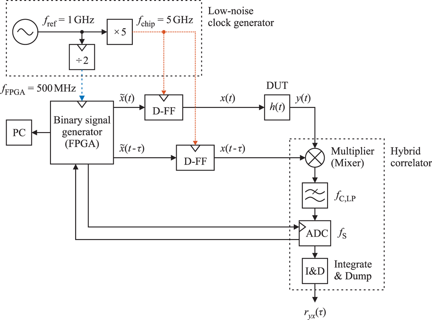
Fig. 3. Block diagram of the developed measurement system with the low-noise binary signal generator and hybrid correlator.
We have already previously used this concept of clock synchronization [Reference Notzon, Storch, Musch and Vogt11]. However, the FPGA clock frequency f FPGA as well as the chip clock frequency f chip were generated using two laboratory signal generators SME06 and SMR40 (Rohde & Schwarz, Munich, Germany) respectively, sharing the same 10 MHz reference oscillator. Inside the generators, PLL concepts are used to achieve a high output frequency. Due to the relatively low reference frequency, high divider factors inside the PLL have to be used, which increase the noise transfer from the PLL components to the output [Reference Mallach, Grys, Musch and Storch13]. Furthermore, the high thermal capacity of the laboratory signal generators leads to a long-term phase drift between the FPGA clock and the clock of the D-FF. Thus, within the long warm-up time of the laboratory signal generators of about 2 hours, the clock synchronization is unstable. Even long-term drifts could be observed, which do not allow for stable measurements over several hours without adjusting the relative phase position.
For a stable clock synchronization, the phase drift between the FPGA clock and the clock of the D-FF has to be below T chip = 200 ps. Furthermore, a small jitter of < 200 fs has to be guaranteed to allow for a high dynamic range without averaging. For a temperature-stable clock frequency, a crystal-controlled oscillator (XCO) is a good option as a reference oscillator. An XCO with additional oven-controlled temperature (OCXO) and integrated frequency multiplier with an output frequency of 1 GHz is available for a reasonable price and used here as a reference oscillator. To increase the clock frequency to the required f chip = 5 GHz, the following two concepts could be used: First, the frequency synthesis by a PLL, secondly, the generation of harmonics by a nonlinear network. The PLL concept uses a temperature-unstable high-frequency oscillator whose phase is related to a temperature-stable low-frequency oscillator. Various concepts for the realization of high-frequency oscillators are available. Yttrium iron garnet-based (YIG) oscillators provide a wide frequency tuning range while maintaining a good quality factor. Since a frequency tuning is not necessary for the measurement system presented here, a dielectric resonator oscillator (DRO) with a very small tuning range and very high-quality factor would be more appropriate. Nevertheless, both types of oscillators require a relatively complex mechanical construction. Alternatively, a voltage controlled oscillators (VCO) realized within an integrated circuit could be used. However, the quality factor is lower and consequently the jitter is higher as compared to the YIG and DRO oscillators. Besides the mentioned oscillators, further electronic circuits (frequency divider, phase detector, loop filter) are required to realize a PLL. For the system realized here, a nonlinear electronic circuit is used to generate harmonics. Subsequently, the desired fifth harmonic is filtered out by using a bandpass filter. A high-quality filter with a large stopband attenuation is required in order to suppress the undesired harmonics. In addition, compared to the above-mentioned laboratory signal generators, the jitter is lower, it is more compact, cost-effective and consumes less power.
The FPGA reference clock at f FPGA = 500 MHz could be derived from the chip clock with f chip = 5 GHz using a  ${\div 10}$ divider. However, since a reference clock with f ref = 1 GHz is available, a
  ${\div 2}$ divider is used, see Fig. 3, which also has even lower requirements for its maximum input clock frequency. The concept and realization of the low-noise clock generator is explained in detail in the section “Low-noise clock generator”.
In the proposed measurement system, shown in Fig. 3, the correlation is performed partly in hardware (time lag and multiplication) and partly in software (precise integration). Thus, no analog integrator is necessary. In addition, the requirements for the sample and hold stage of the analog-to-digital converter (ADC) are low as the mixing and low pass filtering significantly reduces the bandwidth of the signal to be sampled [Reference Notzon, Polzin, Storch, Musch and Vogt10]. For the precise integration over one code repetition period T code or integer multiples thereof, the sampling rate f s has to be an integer multiple N sample of the code repetition frequency:
 $$f_{\rm s} = \displaystyle{{N_{\rm sample}}\over{T_{\rm code}}} = \displaystyle{{N_{\rm sample} \cdot f_{\rm chip}}\over{N}}.$$
The ADC has a maximum sampling rate of 5 MHz. In case of an APAS with a length N = 64,320, for example, N sample = 64 is set resulting in a sampling rate f s ≈ 4.98 MHz.
Low-noise clock generator
Concept
In Fig. 4, a block diagram of the proposed low-noise clock generator including the FPGA and a 10 MHz clock outputs, is shown. The used components are listed in Table 1. As reference signal, a low-noise 1 GHz high-frequency oven-controlled crystal oscillator (OCXO) with a measured output power of approximately 12 dBm into a 50 Ω load is used. The low clock frequencies, f FPGA = 500 MHz for the FPGA and f DSO = 10 MHz for a DSO, used for additional time domain measurements in the section “Low-noise binary signal generator”, are derived from the OCXO using low-noise frequency dividers. This keeps the requirements for the maximum input frequency of the frequency dividers low. The minimum recommended input power of the divider HMC394 is only − 15 dBm allowing to use a double microstrip coupler with a small coupling factor of approximately − 18 dB and a small insertion loss of approximately only − 0.34 dB. As a consequence, a sufficiently large signal level for the frequency multiplier is available. The spectrum of the OCXO output shows significant spurious at every integer multiple of 100 MHz. To suppress the spurious, a surface acoustic wave (SAW) band pass filter with a small − 3 dB bandwidth of 48 MHz is used. After passing the SAW filter, the required input level range of the passive × 5 multiplier is directly available with no need for further attenuation or amplification. Because the multiplier is a passive device, the conversion loss is larger than 25 dB. Spectral components at odd integer multiples of 1 GHz have similar power levels. A designed 4th-order microstrip band pass filter with a center frequency of approximately 5 GHz and a − 3 dB bandwidth of approximately 300 MHz in combination with a low temperature cofired ceramic (LTCC) band pass filter is used to suppress the unwanted spectral components. Due to the high conversion loss of the multiplier and the attenuation of the band pass filters, a low-noise amplifier (LNA) is used to increase the signal level. The LNA is placed right after the passive multiplier to avoid a degradation of the phase noise due to the noise floor and the attenuation of the filters.

Fig. 4. Block diagram of the developed low-noise chip clock generator with additional divider providing low frequency clocks.
Table 1. Components used for the proposed low-noise clock generator.

Realization
In Fig. 5, a photo of the realized PCB including the coupler and the frequency divider is shown. A low-loss RO4003C (Rogers Corporation, Chandler, USA) substrate material (0.2 mm thickness) has been used and mechanically stabilized by a 3D printed frame. The division factor of the HMC394 can actually be changed between 2 and 32 by means of onboard switches. In Fig. 6, a photo of the realized × 5 multiplier with filters and amplifier, which has been realized using the same substrate material, is shown. Sub-miniature-A (SMA) connectors are used to flexibly interface the components and the further test equipment.

Fig. 5. Photo of the realized coupler and frequency dividers.

Fig. 6. Photo of the realized × 5 multiplier.
Measurement results
To verify the functionality of the × 5 multiplier, in a first step, the output spectrum was measured using an FSWP (Rohde & Schwarz, Munich, Germany), see Fig. 7. At f chip = 5 GHz, a large spectral line with the largest power level of approximately − 6.8 dBm can be seen. This level is large enough to trigger the used D-FF HMC723LP3E (Analog Devices, Norwood, USA) even behind a − 6 dB power divider. Spurious lines at integer multiples of the reference frequency f ref = 1 GHz and the transformed spurious of the OCXO at integer multiples of 100 MHz, on the other hand, are strongly suppressed.

Fig. 7. Measured frequency spectrum of the × 5 multiplier output.
In another step, phase noise measurements using the FSWP have been performed, to quantify the jitter. The measured raw data were processed by using a spurious reduction and smoothing algorithm. Fig. 8 shows the single side band phase noise L dB as a function of the offset frequency f os. For a frequency multiplication by a factor of five, a 20 dB log (5) ≈ 14 dB increase of the phase noise is expected [Reference Robins14]. The measured phase noise at the output of the proposed × 5 multiplier output, using the 1 GHz OCXO as the reference, fits well with this theoretical expectation. The band pass filters even decrease the phase noise for offset frequencies down to approximately 10 MHz. In comparison to the laboratory signal generator SMR40, with a comparable output power level of − 5 dBm, the phase noise of the proposed × 5 multiplier is much lower except in the range from  ${1.5\,{\rm MHz}}$ to 27.5 MHz. The standard deviation t j of the jitter was calculated from the measured phase noise by using the following relationship [Reference Kester15]:
 $$t_{\rm j} = \displaystyle{{\sqrt{2 \islant 20% \int_{\,f_{\rm l}}^{\,f_{\rm u}} L(\,f_{\rm os}) \, {\rm d}f_{\rm os}}}\over{2 \pi f_{\rm c}}}, \quad {\rm with } \ L(\,f_{\rm os}) = 10^{L_{\rm dB}(\,f_{\rm os})/10}.$$
The lower and upper limits f l and f u, respectively, of the relevant frequency range have to be specified for calculating t j. The lower limit f l depends on the measurement time and the upper limit f u depends on the receiver bandwidth. Furthermore, the DUT can further limit the bandwidth and accordingly the integration interval in (11). Exemplary, for f l = 1 kHz and f u = 2 GHz, a jitter t j,×5 ≈ 24.3 fs for the × 5 multiplier and a larger jitter t j,SMR40 ≈ 520.2 fs for the SMR40 laboratory signal generator are given.

Fig. 8. Measured phase noise.
Low-noise binary signal generator
Hardware realization using an FPGA
For the realization of the signal generator, a Cyclone V GT FPGA Development Board (Intel, Santa Clara, USA) has been used. This FPGA offers a number of 12 onboard transmitters with a maximum clock rate of 5 Gchip/s. Fig. 9 shows a block diagram of the developed FPGA system. To allow for the high chip frequency f chip = 5 GHz, an integrated PLL is used to multiply the FPGA clock frequency f FPGA. Onboard serializers convert a 40 bit parallel data stream into a serial one, what reduces the internal FPGA clock frequency by a factor of 40 to 125 MHz. In the proposed design, actually four of the available transmitters are used. To feed the corresponding serializers, the data are calculated by four different algorithms, see Fig. 9, which are presented below.

Fig. 9. Block diagram of the developed FPGA system.
The unshifted sequence algorithm continuously repeats the desired excitation sequence, and the shifted sequence algorithm outputs a second sequence with a circular shift relative to the first one. The accordingly realizable time lags are set in steps of the chip period T chip = 200 ps in the digital electronics. The shifted and unshifted sequence algorithms are using independent memory blocks inside the FPGA, which increases the flexibility for generating different types of sequences. Although both algorithms were kept as short as possible, the worst-case propagation delay on the FPGA is approximately 11 ns. Since this is too large for the short clock period of 8 ns, the algorithms are working at half the clock frequency. To achieve the required data throughput under this condition, a factor two larger number of 80 bit is processed in each clock period. Despite this concept, the additional increase of overall propagation delay is still sufficiently small. To be able to feed the serializers, a multiplexer (MUX) inside the FPGA is used to finally reduce the bus width to the required 40 bit.
The shifted sequence algorithm is described in the form of a pseudocode in Algorithm 1. During initialization, the sequence length N, the number of shifts N shifts to be performed, the memory block width W mem, and the cache width W cache are predefined. In the realized system, W mem = 256 and W cache = 80 are given. For a better understanding some iterations of the algorithm, with N = N shift = 7, W mem = 4, and W cache = 3 as an example, are shown in Fig. 10 and are explained below in some more detail. In the left part of Fig. 10, the numerical values of the five variables (n out, k, r, n shift, p shift) at the end of each iteration are given. In the upper part, a periodically stored sequence s = s 0…s 6 with a length N = 7 in memory 2 is shown. In the right part of Fig. 10, the black-rimmed cache content, with the result of the calculations, is given for each iteration. The beginning of a circularly shifted sequence is marked with a black background and the end is marked with a gray background. In the first two iterations, the cache is filled stepwise with the content stored in the memory 2. If the end of the sequence is reached (k ≥ 0), a circular shift operation is performed. The idea behind this algorithm is to rearrange the cache content, as is indicated by arrows in Fig. 10. If a shift occurred, the readout of memory 2 continues at bit position p shift. If k = 0, which happens for example at iteration 7, no cache rearrangement has to be performed. For achieving a high dynamic range, a long sequence length N is required, resulting in a long measurement time. If the IRF of a DUT is significantly shorter than the unambiguous range given by the selected code sequence, the measurement time can be decreased by performing only the necessary number of shifts. In the presented algorithm, in addition, to perform all possible number of shifts (N shifts = N), as was done in the example here, the number of shifts N shifts can be reduced to any integer multiple of the cache width W cache where no cache rearrangement is performed (k = 0), in order to decrease the measurement time.

Fig. 10. Numerical example of the shifted sequence algorithm.
Algorithm 1 Shifted sequence with example values.

For the correlator concept proposed in the section “System overview”, the low pass filter, see Fig. 3, has to be able to settle after each shift operation [Reference Notzon, Polzin, Storch, Musch and Vogt10]. Thus, the sequence is sent twice for each cyclic shift. This is realized by simply repeating the sequence once and by specifying its length twice as long as it actually is. Sometimes, the cache requires content from two adjacent memory blocks right after a shift has been performed, see iteration 6 in Fig. 10. The utilized Cyclone V GT FPGA allows a parallel memory block readout at two independent addresses. This is used here to be always able to readout two adjacent memory blocks, allowing it to keep the algorithm simple and fast.
The algorithm for the unshifted sequence can easily be derived from the shifted sequence algorithm and is much simpler, because no cache rearrangement has to be performed and no shift counter n shift is needed. At the end of the sequence, p shift is set to k.
In addition to the sequence algorithms, two different trigger algorithms were developed. Trigger 1 indicates the start of a measurement (τ = 0) and trigger 2 indicates a shift in time lag τ. In order to synchronize all four algorithms, they get the same enable signal.
Measurement setup
Figure 11 shows a block diagram of the realized measurement setup. The low-noise clock generator described in the section “Low-noise clock generator” is used here to synthesize the low-noise chip clock, the FPGA clock, and the DSO clock. The generated unshifted signal  ${\tilde x(t)}$ and the shifted signal
  ${\tilde x(t-\tau )}$ are clock synchronized to the low-noise chip clock. A − 6 dB power divider is used to distribute the low-noise chip clock signal. The utilized D-FF allow for a chip rate up to 13 Gchip/s, and the single-ended output voltage swing of ± 300 mV results in an output level of approximately 2.6 dBm into a 50 Ω load. In addition, the phase difference between the clock inputs of the two D-FF is adjusted once by using a variable delay line to ensure a stable time shift between clock and data input.

Fig. 11. Block diagram of the measurement setup.
In Fig. 12, a photo of the realized measurement setup is shown. An adapter card XTS-HSMC (Terasic, Hsinchu City, Taiwan) is used to connect the transmitters of the FPGA to SMA connectors and cables. Furthermore, the two D-FF have been shielded by using separate metallic boxes to minimize crosstalk.

Fig. 12. Photo of the measurement setup.
Measurement results
For sampling the time-domain signals x(t) and x(t − τ), a high-speed DSO RTO1044 (Rohde & Schwarz, Munich, Germany) with an input bandwidth of 4 GHz and a sampling rate of 20 GSPS was used. With the realized low-noise and flexible binary signal generator different kinds of sequences can easily be synthesized and tested. For demonstration purpose, an MLS with a large length  ${N_{\rm MLS} = 65,\!535}$ and an APAS with a similar length
  ${N_{\rm APAS} = 64,\!320}$ have been implemented. Sections of both signals with stepwise changed time lags τ from zero to T chip = 200 ps are shown in Fig. 13. In order to decrease the noise of the DSO, 100 measurements were averaged. Both types of sequence, the MLS in Fig. 13 (top) and the APAS (bottom), clearly show the intended and programmed change of the time τ from zero to T chip at the time instance t = 3 ns. Because of the limiting bandwidth of the DSO, the actually shown slew rate of the D-FF is smaller than the actually given one.

Fig. 13. Sections of the measured signals x(t) and x(t − τ) using an MLS of length  ${N_{\rm MLS} = 65,\!535}$ (top) and an APAS of length
  ${N_{\rm APAS} = 64,\!320}$ (bottom).
For another measurement, the proposed hybrid correlator, shown in Fig. 3, instead of the DSO has been used. A through connection has been used as ideal DUT and the bandwidth of the response signal was not limited to 2.5 GHz for the measurement (y(t) = x(t)), in order to directly assess the ACF. Sections of the measured ACF obtained with the same two sequences as above are shown in Fig. 14. To compensate the constant side maxima level of the MLS and the additional DC-level caused by the analog electronics, the mean value of the ACF was calculated in the range  ${0.6\,{\rm \mu} {\rm s} \leq \tau \leq 1\,{\rm \mu} {\rm s}}$ and then subtracted from the ACF in the whole range
  ${\tau \leq 1\,{{\rm \mu} {\rm s}}$. For the MLS, nonlinearities inside the system lead to multiple time-delayed and attenuated MLS, which appear as discrete peaks in the ACF [Reference Ahmad, Guermandi, Medra, Thillo and Bourdoux3] and strongly decrease the achieved dynamic range to approximately 54 dB. In the case of the APAS, nonlinearities also lead to a degradation of the correlation properties. Instead of discrete peaks, the side maxima level is almost evenly increased [Reference Ahmad, Guermandi, Medra, Thillo and Bourdoux3]. Thus, a dynamic range of approximately 65 dB has been achieved.

Fig. 14. Sections of the measured ACF r xx(τ) using an MLS of length  ${N_{\rm MLS} = 65,\!535}$ and an APAS of length
  ${N_{\rm APAS} = 64,\!320}$.
We have already previously measured the ACF [Reference Notzon, Storch, Musch and Vogt11]. But instead of the hybrid correlator approach, we have sampled the high-frequency signals x(t) and x(t − τ) using the relatively expensive DSO RTO1044 and performed the correlation in software. We have shown that a dynamic range of at least 90 dB can be achieved using the proposed binary coded signal generator.
The limitations by measuring the ACF with the hybrid correlator are due to the nonlinearities inside the mixer SYM-63LH+ (Mini-Circuits, Brooklyn, USA) used for multiplying the signals in hardware. A compensation of these nonlinearities is challenging, because their impacts on a measured IRF depends on the DUT behavior. Furthermore, a high pass characteristic of the baluns, which are included in the mixer, further limit the dynamic range for  ${\tau < 0.1\,{\rm \mu} {\rm s}}$. A further optimization of the proposed correlator regarding the linearity has to be done in order to take advantage of the presented low-noise binary signal generator. This is currently under investigation.
Conclusion
In this contribution, a flexible and low-noise binary coded signal generator based on an FPGA was presented. A clock generator with low-noise was realized and validated by means of phase noise measurements. A small jitter t j,×5 ≈ 24.3 fs within an integration range from 1 kHz to 2 GHz could be achieved. This generator allows for a low-noise and long-term stable signal generation. Furthermore, an algorithm for fast and precise shifting of the time lag between two binary coded signals was shown, which allows for correlating excitation and response signals in the proposed hybrid correlator. Finally, the realized demonstrator system has been tested using two commonly used types of binary coded sequences, the maximum length sequence and the almost perfect autocorrelation sequence.
 Gordon Notzon was born in Hamm, Germany in 1986. After completing an apprenticeship as an Information and Telecommunication Systems Engineer at Deutsche Telekom AG, he received the B.Sc. and M.Sc. degrees in electrical engineering and information technology from Ruhr University Bochum, Bochum, Germany, in 2012 and 2013, respectively. Since November 2013, he has been a Research Assistant with the Institute of Electronic Circuits, Ruhr University Bochum. His current research interests include the design of time domain reflectometry measurement systems based on binary coded signals with high bandwidth, high accuracy, and high precision.
 Robert Storch was born on January 28, 1983, in Waldbröl, Germany. He received the Dipl.-Ing. degree in electrical engineering and the Dr.-Ing. from the Ruhr University Bochum, Bochum, Germany, in 2008 and 2015, respectively. From 2008 to 2015, he was with the Institute of Electronic Circuits at the Ruhr University Bochum. His main areas of research were microwave and low frequency synthesis as well as the development of concepts and circuits for ultra-wideband and FMCW radar systems. In 2015, he joined Krohne Innovation GmbH, Duisburg, Germany, as an R&D engineer, where he is working on radar level measurement systems and time domain reflectometry systems.
 Thomas Musch was born in Mülheim Ruhr, Germany, in 1968. He received the Dipl.-Ing. and Dr.-Ing. degrees in electrical engineering from Ruhr University Bochum, Germany, in 1994 and 1999, respectively. From 1994 to 2000, he was a Research Assistant with the Institute of High Frequency Engineering, Ruhr University Bochum, where he was involved in system concepts and electronic components at microwave frequencies, mainly in the fields of frequency synthesis and high-precision radar. From 2003 to 2008, he was with Krohne Messtechnik GmbH, Duisburg, Germany. As the Head of the Department of Corporate Research, he was responsible for research activities with the Krohne Group, Duisburg, Germany. In 2008, he became a Full Professor of electronic circuits with Ruhr University Bochum. His current research interests include frequency synthesis, radar systems and antennas for microwave range finding, industrial applications of microwaves, and automotive electronics.
 Michael Vogt received the Dipl.-Ing. degree in electrical engineering and the Dr.-Ing. degree from the Ruhr University Bochum, Germany, in 1995 and 2000, respectively. From 1995 to 2016, he was a Research Assistant with the High Frequency Engineering Research Group, and since 2016 he is with the Institute of Electronic Circuits, both also at the same location. In 2008, he qualified as a university lecturer (Habilitation), and he was appointed in 2018 as an Adjunct Professor by the Faculty of Electrical Engineering and Information Technology of the Ruhr University Bochum. His main areas of research are microwave and ultrasound measurement and imaging systems, antennas, signal and image processing, and high frequency electronics. In 2007, he joined Krohne Messtechnik GmbH, Duisburg, Germany, as an R&D engineer, where he is working on electromagnetic level measurement systems, ultrasonic flowmeters, and sensor systems.


