I. INTRODUCTION
In contemporary world, intensive determinations have been made worldwide for the application of gigabit fidelity (Gi-Fi) data rate wireless communication system in the frequency band of 60 GHz. Distinct features of the radio propagation in this frequency band are high penetration loss of construction materials and severe oxygen absorption, and broadband spectrum makes it suitable for the deployment of high data rate short-distance communications [Reference Smulders1–Reference Rappaport, Murdock and Gutierrez4]. A high-frequency band leads to a small size of radio frequency (RF) components, including antennas. Recently, the IEEE 802.15.3C was formed to standardize the 60 GHz wireless personal area network (WPAN) systems, which will allow high data rate up to 3 Gbps [5]. The 60 GHz technology offers various recompenses over the present wireless communication systems. One of the deciding factors that mark the 60 GHz technology gaining significant interest recently is due to the huge unrestricted bandwidth (up to 7 GHz) available worldwide. This huge bandwidth represents great potentials in terms of capacity and flexibility that makes 60 GHz technology mainly attractive for Gi-Fi wireless applications [Reference Smulders and Wagemans6, Reference Kyro7]. However, many challenges have to be overcome before designing the system, such as cost and complexity implementation of such systems requires a suitable antenna solutions and channel model for the characteristics of the 60 GHz radio propagation, which can be used for the RF front-end. Therefore, this work targets on design and development dielectric-loaded exponentially tapered slot (ETS) antenna using substrate-integrated waveguide (SIW) technology particularly at 60 GHz. Further developed antenna is used to measure indoor propagation characteristics.
This paper is organized as follows: Section 2 deals with antenna design, simulation, prototype, and measurement results. Section 3 deals with Channel measurement, characterization, and result analysis. Finally, Section 4 gives conclusions.
II. DIELECTRIC-LOADED SIW ETS ANTENNA DESIGN
Antennas with excellent design can improve the performance of wireless communications, particularly at millimeter wave (MmW) frequencies. Many types of antenna structures are considered not suitable for 60 GHz applications due to the requirements for low cost, small size, and light weight. In addition, 60 GHz antennas also require to be operated with constant gain and high efficiency over the broad frequency range [Reference Huang and Edwards8]. In addition, the traditional waveguide technique cannot be used to reduce weight and volume [Reference Deslandes and Wu.9]. The concept of SIW technology makes it possible to realize the waveguide in a substrate and provides a sophisticated way to integrate the waveguide with MmW planar circuits using the conventional printed circuit technology. In particular, a number of SIW-based slot antennas have been reported in recent years [Reference Ramesh and Rao10, Reference Hosseininejad, Komjani, Oraizim and Noghani11]. These antennas consist of single layer of the dielectric substrate and are fed from one end through a coplanar feed network, which significantly increases the size of the antenna [Reference Rezaiesarlak, Salehi and Mehrshahi12].
The ETS antenna is known as flared notch antenna and satisfying all the requirements. A major advantage of this antenna is that wide bandwidth and maximum gain can be achieved using exponentially tapered profiles with dielectric loading [Reference Gazit13]. This antenna is integrated using a single substrate. To eliminate the higher order modes in the waveguide, the thickness of the substrate is restricted. The loaded dielectric slab in front of the antenna can be considered as a dielectric-guiding structure excited by exponential flare resulting in a wider beamwidth and maximum gain. The compact MmW antenna with dielectric loading can achieve a broadband performance and offer several advantages over other counterparts such as relatively low insertion loss, better voltage standing wave ratio (VSWR), good design tolerance, and circuit size compactness [Reference Ghassemi and Wu14].
A) Replacing waveguides with equivalent SIW
At MmW frequencies waveguide devices are preferred but manufacturing process is challenging. Hence, the SIW technology makes it possible to realize the waveguide in a substrate and provides a sophisticated way to integrate the waveguide with MmW planar circuits [Reference Wu, Deslandes and Cassivi15, Reference Xu and Wu16]. In the SIW design, the following conditions are required:
The metalized via hole diameter is
 $$d \lt {\lambda _g} / 2.$$
The spacing between the via holes is
 $$P \lt 2d.$$
The physical width of SIW is
 $$a = {a_d} + ({d^2} / (0.95p)).$$
B) Design of the antenna
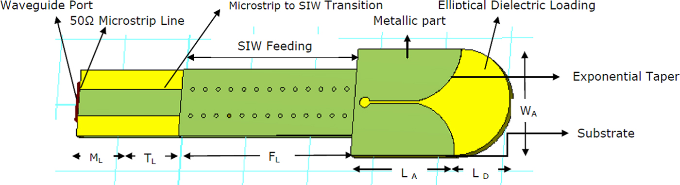
The ETS antenna radiating tapered profile is described by an exponential function. The antenna is excited via the microstrip line to SIW transition. The transition construction exploits wideband features of a microstrip radial stub used as a virtual wideband short. The microstrip is virtually shunted to the second half of the strip line metallization, while the first half serves as a ground metallization for the microstrip line. It is necessary to transform the impedance of the input feeding microstrip line to the input impedance of the transition. Therefore, the linear microstrip taper is used as the input impedance transformer. Instead of using the wideband balun, a SIW has been employed to feed the antenna.
To comply with the antenna board dimensions and slot line parameters, following exponential taper curve definition equation is used [Reference Yang, Wang and Fathy17, Reference Hood, Karacolak and Topsakal18]:
 $$y = {C_1} e^{a x} + {C_2},$$
where “a” is the rate of opening the exponential taper, and C 1 and C 2 can be calculated by the starting and ending points of the taper P1(x 1, y 1) and P2(x 2, y 2),
 $${C_1} = ({y_2} - {y_1})/({e^{a x_2}} - {e^{a x_1}}),$$
 $${C_2} = ({y_1} {e^{a x_2}} - {y_2} {e^{a x_1}})/({e^{a x_2}} - {e^{a x_1}}).$$
Figures 1–3 illustrate layout of a modeled SIW-based ETS antenna without, rectangular, and elliptical dielectric loading, respectively.
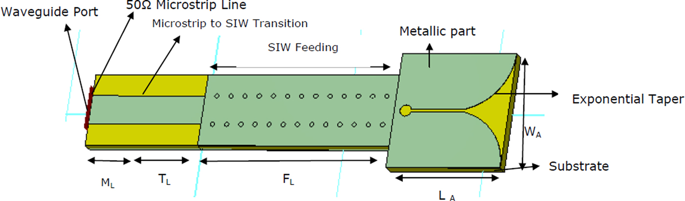
Fig. 1. ETS antenna without dielectric loading.
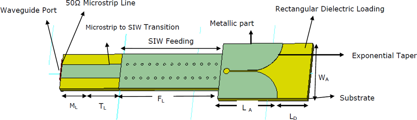
Fig. 2. ETS antenna with rectangular dielectric loading.

Fig. 3. ETS antenna with elliptical dielectric loading.
Table 1 shows the parameters of the antenna obtained using above equations. The shape of the curvature influences the traveling wave in two main areas. First is the beginning of the taper and the second is the wide end of the taper. On both places, a reflection of the traveling wave is likely to occur. Therefore, smoother taper in the neck minimizes the reflection there [Reference Hamzah and Othman19]. This can be achieved with higher value of “a”. The beamwidth in the H-plane can be controlled through the flare in the H-plane. The beamwidth in the E-plane is determined by the flare in the E-plane that is limited. In some applications, a wider beamwidth in the E-plane is also desired. For this purpose, a dielectric slab is placed in front of the antenna. This slab serves as the dielectric guiding structure in the E-plane. In the H-plane, for an antenna with maximum gain, the flare phase distribution along the H-plane is nearly uniform without the dielectric loading.
Table 1. Dimension of the antenna

C) Simulation and measurement results discussions
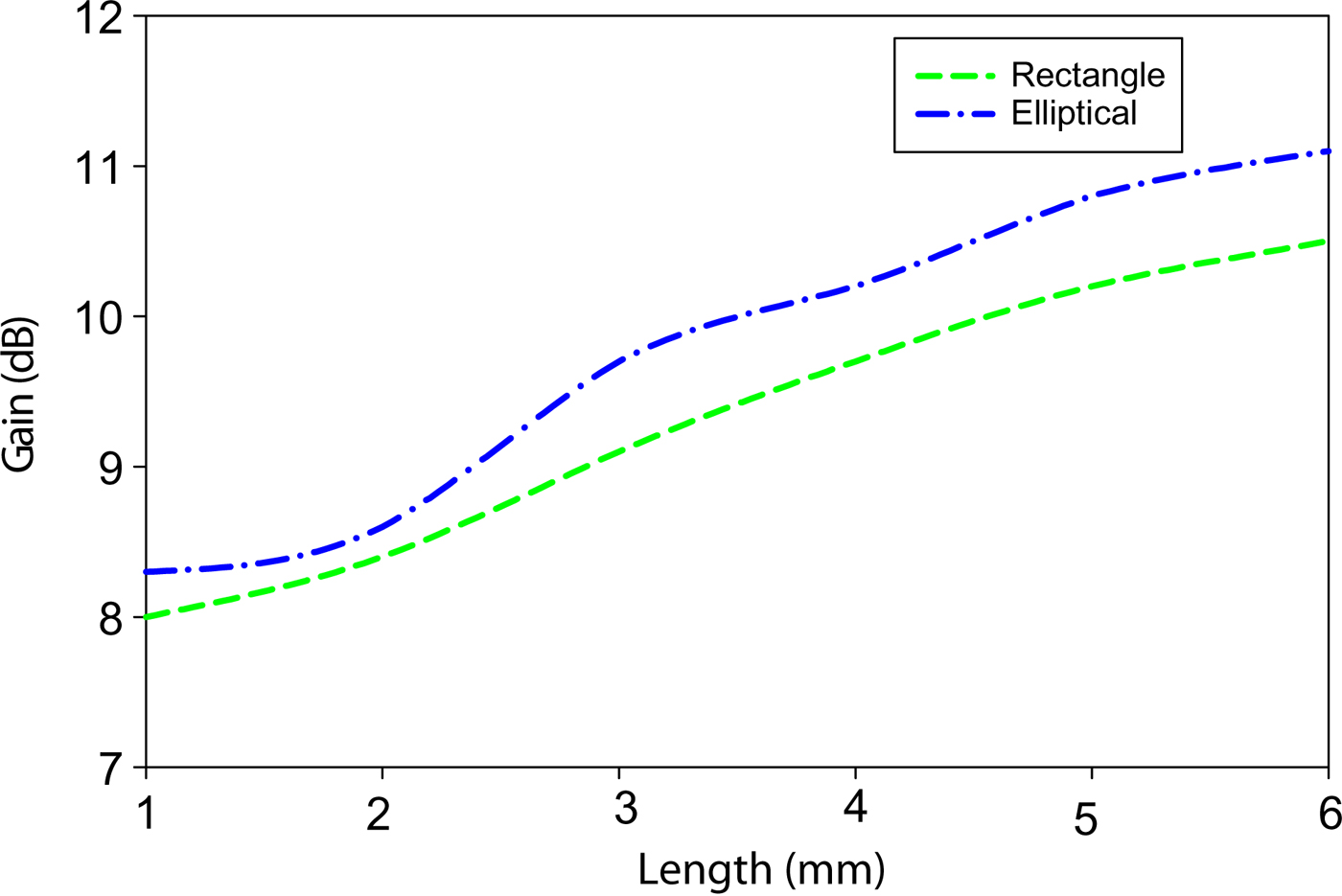
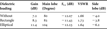
The antenna structure is simulated without dielectric loading using three-dimensional (3D) electromagnetic (EM) software CST Microwave Studio as shown in Fig. 2, the gain is 7.2 dB, main lobe direction is 81°, return loss is −12.07 dB, VSWR is 1.66 and side lobe level is −4.0 dB. A rectangle and elliptical dielectric loading is placed in front of the antenna flare to increase the gain, reduce the side lobe level of the antenna and respective structures are shown in Figs 3 and 4.

Fig. 4. Gain versus length of the dielectric loading.
Figure 4 shows that the elliptical dielectric loading gives higher gain compared with the rectangle dielectric loading with the same length. When the length of dielectric loading is 4 mm, gains of rectangle and elliptical are 8.3 and 11.4 dB, respectively. Furthermore, the rectangle and elliptical dielectric loading are investigated. Table 2 shows the performance comparison of the dielectric loading at 60 GHz. The dielectric-loaded antenna was suggested in [Reference Ramesh and Rao20] which are useful in high-gain applications. However, in the dielectric-loaded antenna using SIW technology provides slightly higher gain with wider main lobe directions at 60 GHz.
Table 2. Performance comparison of the dielectric loading at 60 GHz

Compared with the antenna without dielectric loading, the gain of the elliptically dielectric-loaded antenna is increased by 4.2 dB, S 11 parameter has decreased by −0.16 dB and the main lobe direction is increased by 24° with less side lobe level. From these results it is seen that the elliptical dielectric loading antenna gives higher gain with the marginally broader main lobe direction at 60 GHz. The performance comparison of the antenna with elliptical dielectric loading using 3D EM software CST and comparisons with high frequency structure simulator (HFSS) validate the design procedure based on antenna gain, S 11, and VSWR. It is observed that there is good agreement in the simulated results between the gain, S 11, and VSWR. A slight difference in the two simulated values is basically because of the two different numerical methods employed in CST and HFSS. Furthermore, the antenna efficiency with elliptical dielectric loading is also analyzed and found that the radiation efficiency is 96.84% and total efficiency is 91.05%.
The antenna without dielectric loading and elliptical dielectric loading with optimized dimensions are fabricated on the Rogers RT Duroid 5880 high-frequency substrate with a thickness of 0.787 mm, relative permittivity of 2.2, and relative permeability of 1 and loss tangent of 0.0009. The top side of the antenna has radiating flare and the other side is ground plane. The photograph of fabricated antenna with elliptical dielectric-loaded ETS antenna is shown in Fig. 5.

Fig. 5. ETS antenna with elliptical dielectric loading.
The antenna S 11 parameter and gain are measured using the Vector Network Analyzer MVNA-8-350 with probe station. The simulated and measured S 11 parameter for antenna with elliptical dielectric loading is shown in Fig. 6. A slight difference is observed between the measured value and simulated value. The difference between the measured and simulated S 11 of the antenna is caused by the microstrip to SIW transition.
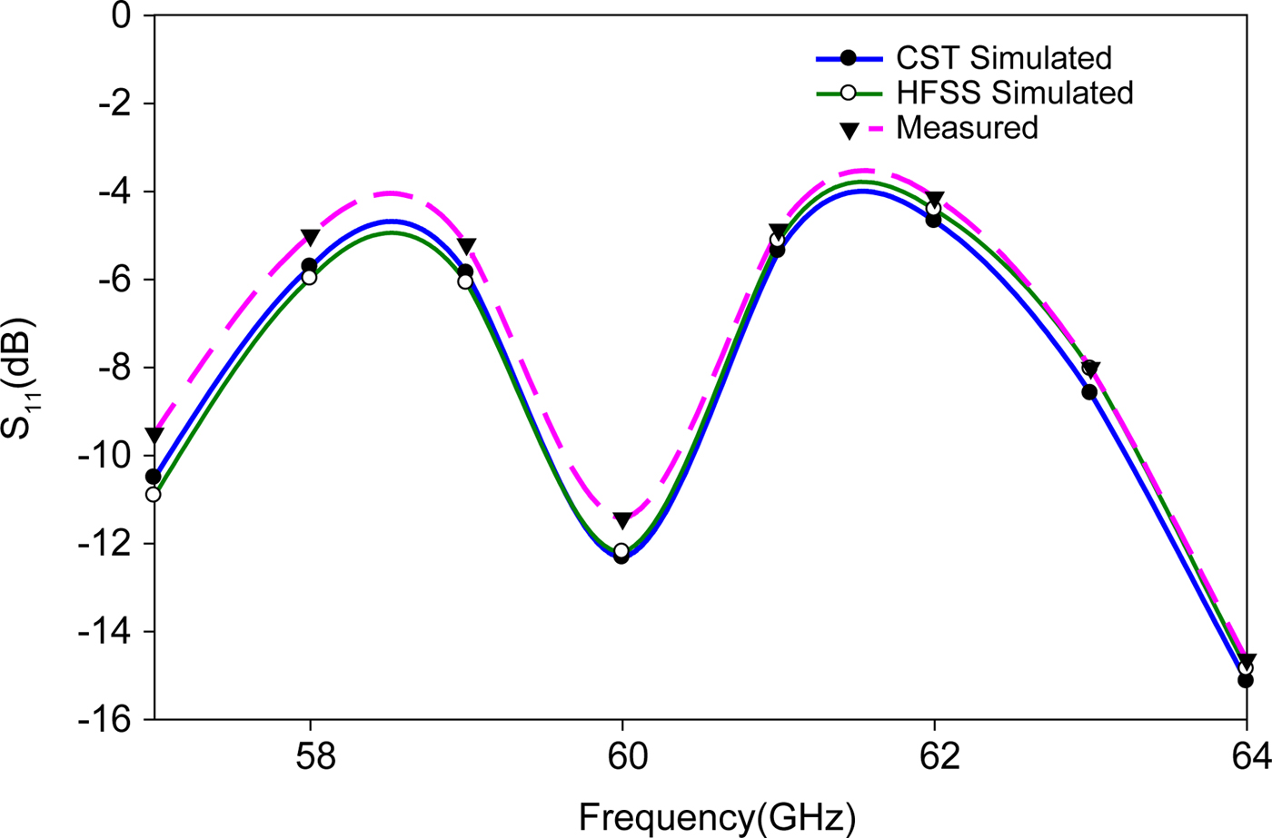
Fig. 6. Measured and simulated S 11 parameter for antenna with elliptical dielectric loading.
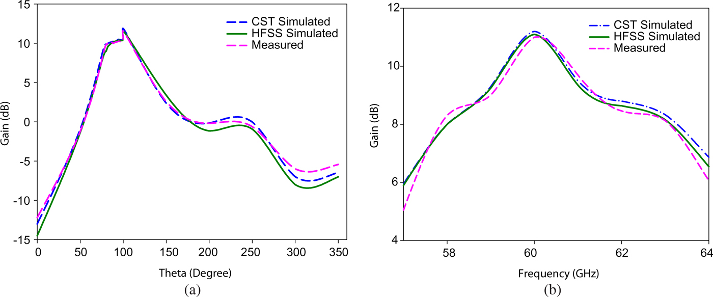
The simulated and measured gain of the antenna with elliptical dielectric loading is shown in Figs 7(a) and 7(b). The maximum of measured gain is also very close with 10 dB at 60 GHz for the antenna and the simulated maximum of gain is 10.2 dB. The measured result shows that the bandwidth of the antenna covers over 3.33 GHz, while the gain of the antenna is kept almost constant within such a wide bandwidth of the antenna. Simulation results specify that metallic and dielectric losses do not have a substantial effect on the bandwidth and matching condition of the antenna, while they decrease the measured gain of antenna by 0.2 dB. The apparent difference between the simulation and measured gains might be due to the calibration-linked tolerance range of the antenna reference in anechoic chamber.

Fig. 7. Measured and simulated gain for antenna with elliptical dielectric loading.
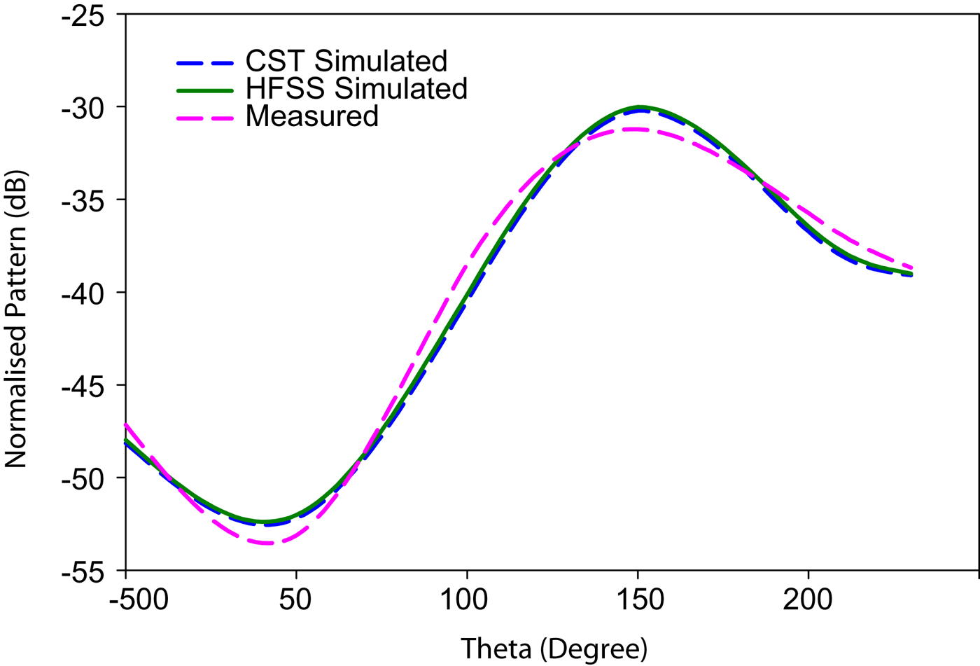
The measured radiation pattern of the antenna at resonant frequency is shown in Fig. 8. The radiation pattern measurement is carried out in a conventional far-field anechoic chamber which uses a V connector to connect the antenna. Owning to the size of the connector compared with the antenna, the rear radiation patterns were not incorporated in the results. However, the similar effects were observed in the simulation results and most significantly, the radiating behavior of the antenna is very similar to simulation results.

Fig. 8. Measured and simulated radiation pattern for antenna with elliptical dielectric loading.
III. CHANNEL MEASUREMENT AND CHARACTERIZATION
The study of wave propagation seems as a significant task when developing a wireless system. The purpose of this section is to focus different aspects concerning the wireless propagation channel at the 60 GHz system. In indoor environments, the radio propagation of EM waves between the transmitter and the receiver is characterized by the occurrence of multipath due to various phenomena such as reflection, refraction, scattering, and diffraction. In fact, the performance of communication systems is largely dependent on the propagation environment and on the structure of antennas [Reference El Zein21, Reference Rappaport22].
A) Measurement setup
The transmitter/receiver pair (Model: TRA-5960FW) with elliptically dielectric-loaded ETS antenna was used to carry out the measurements in the narrow hallway environment. To generate 60 GHz frequency, a reference signal of 10 MHz for phase locked loop (PLL) locking and an intermediate frequency (IF) of 3 GHz were fed to the transmitter. Power was fed to the transmitter through a signal generator (Agilent's N5182A MXG). The receiver was connected to the spectrum analyzer (Agilent's N9010A EXA) with the span set to 50. The control and data storage were also accomplished by the spectrum analyzer. The transmitter and receiver antennas were mounted on a controllable positioning device at the height of 1 m. By the help of this positioner, the antenna could be moved accurately over a certain distance on a linear track during the measuring procedure. During the acquisition the receiver antenna was moved over a distance of 10 m.
B) Description of simulation environment and measurement
Narrow corridor environment holds the following dimensions, 14.0 m length, 1.83 m width, and 3 m height, in a modern multi-storied building. The left and right walls of the narrow hallway is made of concrete (relative permittivity ε r = 7.0) with glass windows (ε r = 4.0). The floor is covered with porcelain tiles (ε r = 6.0) and the concrete ceiling is covered with gypsum board (ε r = 3.0). Figure 9 illustrates the 3D view of narrow corridor environment. The hallway is located on the 13th floor of the Tech Park building of SRM University, Chennai, India (GPS Coordinates: 12° 49′ 29.35″N, 80° 02′ 42.88″ E) [Reference Kumar and Rama Rao23].

Fig. 9. (a) Three-dimensional design of narrow corridor environment. (b) Narrow corridor environment. (c) Measurement setup for narrow corridor environment using Horn antennas for reference. (d) Measurement setup for narrow corridor environment using elliptically dielectric-loaded ETS antenna.
C) Analytical parameters
The value of the received power obtained from measurements is converted into path loss (PL). The PL at a distance d from the transmitter is [Reference Rappaport22]
 $$P_{RX} ({\rm dBm}) = P_T - PL_d + G_T + G_R,$$
where P T is the transmitted power in dBm, PL d is the path loss in decibels for the transmitter–receiver separation distance d, P RX is the received power measured in dBm, G T is the transmit antenna gain in decibels, and G R is the receive antenna gain in decibels. Path loss exponent (PLE) can be derived from the calculated value of the path loss. The PLE is given by [Reference Rappaport, Murdock and Gutierrez4].
 $$PL_d({\rm dB}) = PL_{d0} + 10n\log \left({\displaystyle{d \over {d0}}} \right) + {X_\sigma},$$
where n is the PLE, d 0 is the reference distance at the transmitter which is 1 m in this case, PL d0 is the path loss at reference distance d 0, d is the distance between the transmitter and receiver, PL d represents the path loss at distance d and X σ is the Gaussian random variable whose average value is zero [Reference Kumar and Rama Rao23] and standard deviation is σ. This parameter shows that the path loss at any given point will deviate from its average value.
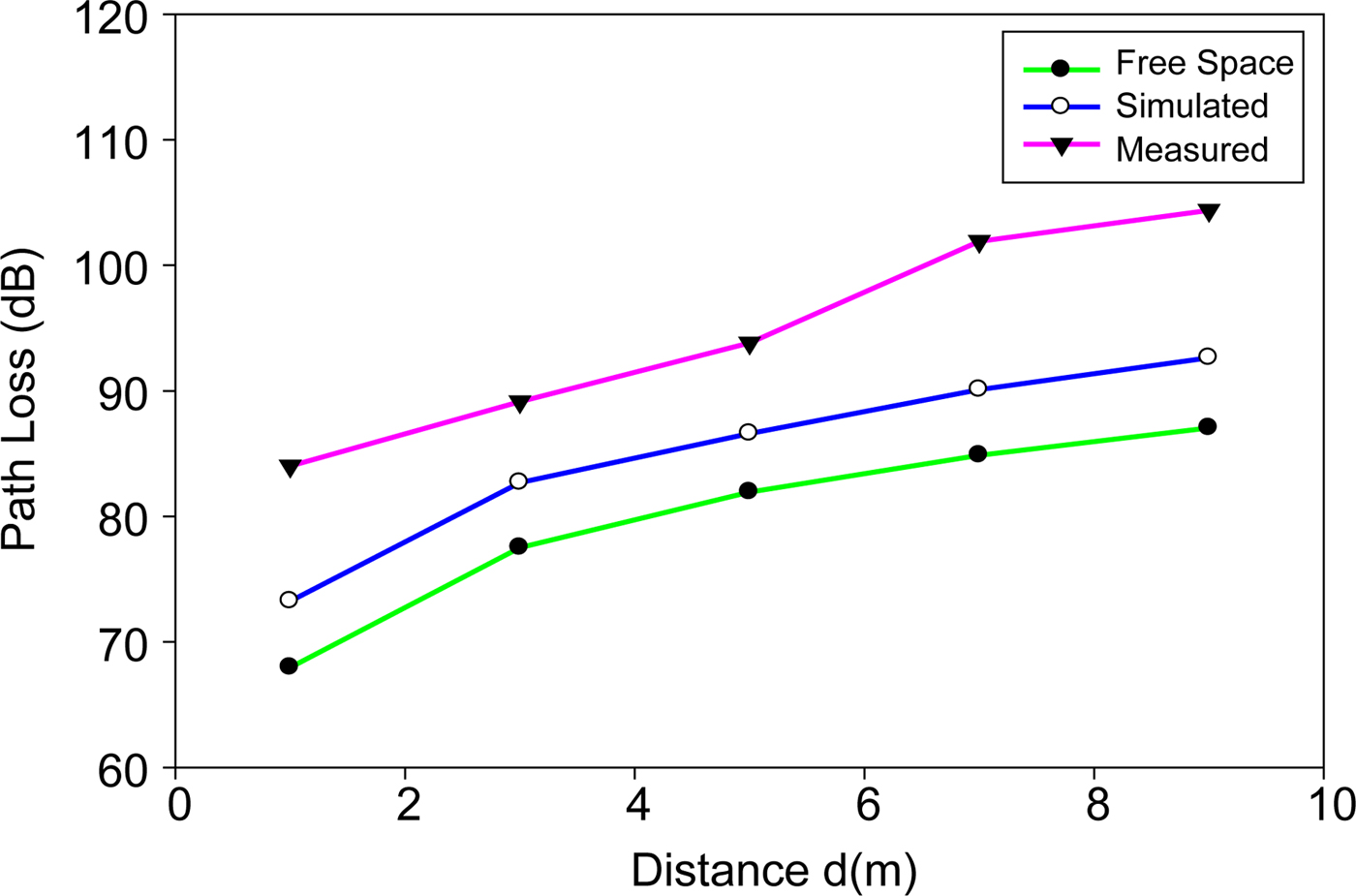
Figure 10 shows the path loss value in narrow corridor environment. For the comparison, the calculated, simulated, and measured path loss values for LOS scenario using dielectric-loaded ETS antenna are given in Table 3. From the results, it is observed that the path loss for narrow corridor environment increases as the transmitter–receiver separation distance increases. It is observed that the path loss varies from 84 to 103 dB in a narrow corridor within an operating space of 10 m. The differences between calculated and measured path loss values are due to presence of ETS antenna V connector, waveguide adaptor and blocking effects. If communication link occurs in a larger box-shaped room then we have to do coverage and planning analysis for to deploy the access points. The path loss will increase further in larger room.

Fig. 10. Path loss values in narrow corridor environment.
Table 3. Summary of Path Loss values in narrow corridor environment

Another important parameter derived from the Power Delay Profile (PDP) is the root-mean-square (RMS) delay spread (DS), is defined as square root of the second central moment of the average PDP and it provides a measure of the variability of the mean delay. At MmW frequencies the channel dispersion is smaller when compared with the values encountered at lower frequencies because echo paths are shorter on average. Measurements at 5 and 60 GHz indicate a difference of a factor 1.5–2. The RMS DS of the channel may range from a few to 100 ns. It is expected to be highest if omnidirectional antennas are used in large reflective indoor environments. When high-gain antennas are used, the RMS DS may be limited to a few ns only, but this is only the case when the antennas are exactly pointed toward each other [Reference Rama Rao, Murugesan, Tiwari and Labay24]. The RMS DS τRMS, which can be expressed as,
 $$\tau _{{\rm RMS}} = \sqrt {\displaystyle{{\sum\limits_{i = 1}^N {\left( {{{\left( {{\tau _i}} \right)}^2} - {{\left( {\overline \tau} \right)}^2}} \right){P_i}}} \over {\sum\limits_{i = 1}^N {{P_i}}}}},$$
where τ
i
and P
i
are the excess delay and the power level of ith multipath component of the PDP, respectively. The
 ${\bar \tau}$
is the first central moment of the PDP and it represents the average excess delay of the channel. Typical values of τ
RMS for indoor environments at 60 GHz are of the order of 10 ns or less.
${\bar \tau}$
is the first central moment of the PDP and it represents the average excess delay of the channel. Typical values of τ
RMS for indoor environments at 60 GHz are of the order of 10 ns or less.
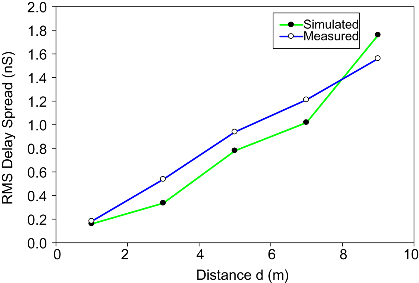
Figure 11 shows the RMS DS in narrow corridor environment. For the comparison, the simulated and measured RMS DS values for LOS scenario using Dielectric-loaded ETS antenna are given in Table 4. The typical values for indoor environments at 60 GHz are of the order of 10 nS or less [Reference Kyro7]. From the results, it is observed that it is expected to be higher if omnidirectional antennas are used in large reflective indoor environments. With the high-gain antennas, the RMS DS may be limited to a few ns only but this is the case only when the antennas are exactly pointed toward each other. This can be attributed to the complex nature of the 60 GHz channel and the diverse range of propagation scenarios confronting each researcher.

Fig. 11. RMS DS in narrow corridor environment.
Table 4. Summary of RMS DS in narrow corridor environment

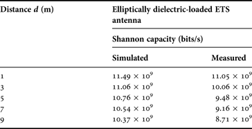
Further effort was made to decide the capacity, the maximum rate at which information can be transmitted. As 60 GHz has the potential to provide the Gbps data rates, it can be used for high definition video streaming multimedia applications. The channel capacity defines the maximum attainable data in the specified channel condition. Capacity is set by bandwidth and signals-to-noise ratio (SNR) and can be given as [Reference Kumar and Rama Rao23, Reference Rama Rao, Murugesan, Tiwari and Labay24].
 $$ C = B \times {\log _2} ({\rm SNR} + 1),$$
where B is the offered bandwidth of the system and SNR is a measure of signal strength relative to the background noise and can be obtained by,
 $${\rm SNR} = P_{RX} - 10\log (KT_{syst}) - 10\log (B) - NF_{RX},$$
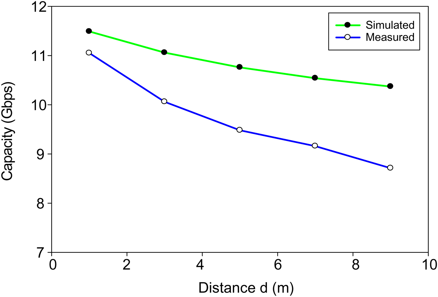
where P RX is the received power, 10 log (kT syst) is equal to 174 dBm/Hz for a system temperature of 17°C, NF RX is the noise figure of the receiver in decibels, and “B” is the bandwidth of signal in hertz. The receiver low noise amplifier (LNA) noise figure is assumed to be 8 dB and the RF bandwidth is assumed to be 3.33 GHz. It is observed that capacity decreases with increasing distance. Table 5 provides the summary of the capacity value in narrow hallway environment. Furthermore, the performed study shows that the ETS antenna has a higher capacity compared with the horn antenna with the maximum capacity of 11.49 Gbps within an operating space of 10 m [Reference Rama Rao, Murugesan, Tiwari and Labay24]. Fig. 12 shows the maximum reachable capacity value in a narrow hallway environment. It is observed that the capacity decreases with increasing distance.

Fig. 12. Maximum attainable capacity value in narrow corridor environment.
Table 5. Summary of capacity value in narrow corridor environment

IV. CONCLUSIONS
The use of MmW techniques offers many advantages for short-range Gi-Fi wireless communication systems compared with radio techniques at lower frequencies. Besides, a new adaptation between microstrip line and SIW is proposed which is predominantly useful in MmW Gi-Fi wireless communication applications. The SIW technology with emulated waveguides can be utilized to eliminate the unwanted radiations from feed, particularly when compared with similar structures built using microstrip lines. A novel configuration of SIW-based ETS antenna with dielectric loading is proposed, designed, fabricated, and measured. The proposed antenna measured gain of the antenna is 11.2 dB, return loss is −12.23 dB, VSWR is 1.64, and main lobe direction is 104° at 60 GHz. It is also observed that with proper selection of dielectric structures and its parameters, marginally more gain with broader main lobe direction for the given antenna can be achieved. The reasonable agreement between the simulated and measured results shows that the designed antenna with elliptical dielectric loading is useful for the variety of wireless applications. In order to support a Gi-Fi reliable transmission within an indoor environment and unembellished multipath dispersion, a suitable solution is to use high-gain antennas. However, our studies exposed that the high-gain antenna directivity stresses the importance of the antennas pointing accuracy. In addition, the use of directional antennas for 60 GHz WPAN applications is very sensitive to objects blocking the LOS path. It is believed that the huge demand for bandwidth and higher data rate services will make the 60 GHz channel an inevitable eventuality. However, due to the complex nature of MmW propagation, there are still a lot of unknowns that need to be quantified before a working standard is achieved. With this in mind the work presented in this paper serves as a valuable contribution to the deployment of MmW-based wireless local area network (WLAN) and WPANs.
ACKNOWLEDGEMENTS
Authors are very much grateful to the DRDO, Government of India for providing financial patronage in executing this research work.
 S. Ramesh currently, working as Assistant Professor in Electronics & Communication Engineering, Valliammai Engineering College, Chennai, India. He received his B.E. degree in Electronics and Communication Engineering from University of Madras, Tamilnadu, India in 2001, M.Tech. degree in Communication Engineering from VIT University, Vellore, Tamilnadu, India in 2004 and Ph.D. degree from SRM University, India in 2015. He is a member of IEEE Antennas & Propagation Society, Life member of Indian Society for Technical Education (ISTE), Institute of Electronics and Telecommunication Engineers (IETE), and Broadcast Engineering Society of India (BES-I). He authored many papers in reputed journals and international/national conferences. His area of interest includes Antennas & Propagation and Wireless Communications.
 T. Rama Rao currently, working as “Professor & Head” of the Telecommunication Engineering Department, SRM University, India. He received his Ph.D. degree on “Radio Wave Propagation studies for Fixed and Mobile Communications over Southern India” from Sri Venkateswara University, Tirupati, India in the year 2000. Professor Rama Rao is a Member of the IEEE; an IETE Fellow; Senior Member of ACEEE, Member of Life Member of the ISCA, Member of IACSIT, Member of ACM and Member of WWRF – Wireless World Research Forum. He was the recipient of “Young Scientist” award for the XXVIth URSI General Assembly, University of Toronto, Canada, held during August 1999. And, he has been selected as a participant to attend the “School on Data and Multimedia Communications using Terrestrial and Satellite Radio links” organized by the ICTP (International Centre for Theoretical Physics), Trieste, Italy, 7–25 February 2000. Dr. Rama Rao worked with Aalborg University, Denmark as “Assistant Research Professor”; with Universidad Carlos III de Madrid, Spain and at the University of Sydney, Australia as “Visiting Professor”. Also, he worked as “Post Doc Research Fellow” at the National Chio Tung University, Hsinchu, Taiwan. He has a long-standing research history on Radio wave Propagation Studies for Wireless Communications. His research interests are Antennas, Radio Channel Measurements & Modeling, Broadband Wireless Communications and Mobile Cellular Telecommunications. He authored papers in reputed journals/transactions and international/national conferences.