


I. INTRODUCTION
GaN HEMTs have proven to be of great interest for the realization of high-power solid-state amplifiers, thanks to their high breakdown field, high electron densities, and high electron saturation velocity. Many results were published showing impressive output powers higher than several hundreds of watts, mostly in the frequency bands L to C [Reference Kim, Kwack and Cho1–Reference Yamanaka, Kimura, Chaki, Nakayama and Hirano9]. Today, such amplifiers based on AlGaN/GaN HEMT technology are already commercialized. However, many developments and researches are being conducted in order to improve the performances, the reliability and the cost of such amplifiers [Reference Joh and del Alamo10–Reference Floriot13].
The InAlN/GaN HEMT technology is more recent and remains at the research level, in several laboratories. [Sentence displaced ] Thanks to its higher spontaneous polarization charges, InAlN/GaN HEMTs can achieve higher sheet carrier densities, i.e. higher output currents compared to AlGaN/GaN HEMTs. This technology also shows advantages in terms of maximum operating temperature [Reference Maier14, Reference Herfurth15] and may offer good reliability thanks to the lattice match between InAlN and GaN layers [Reference Kuzmik16, Reference Kuzmik17]. However, some work remains to assess this latter point more in depth, which can be done only after stabilization of the technological processes. Nevertheless, very high-power densities have already been demonstrated with InAlN/GaN HEMTs and particularly at high frequencies (X to Ka bands) where they can have advantage over AlGaN/GaN HEMTs, thanks to thinner barrier layers leading to a reduction of the short channel effects [Reference Sarazin18–Reference Jardel20].
The aim of the study presented here is to evaluate the interest of this technology at lower frequency bands, and particularly in the case of very high-power amplifiers, where thermal management is critical. InAlN/GaN transistors could then have assets, considering their capability to sustain high temperatures. Thus, we present power results obtained on L-band packaged amplifiers using this transistor technology.
First measurements results presented in [Reference Piotrowicz21] demonstrated a record output power of 105 W in the cw mode and 140 W in the pulsed mode at V ds = 30 V on a single die amplifier. Additional results obtained at higher bias voltages on the single-die amplifier and new results based on a double die version are presented here. In cw mode, these results were obtained thanks to an improved thermal management, which includes improvements at the chip level, at the interface between the chip and the package with the use of the diamond-based heat spreader, as well as at the package and carrier levels. This will be detailed in the measurements section.
II. EPITAXIAL GROWTH AND TECHNOLOGICAL PROCESS
The HEMT structure was grown using a metal-organic chemical vapor deposition reactor (MOCVD) on a 4H–SiC substrate. A 1.7 µM thick GaN buffer layer, an AlN thin spacing layer of 1 µm and an undoped In0.21Al0.79N layer of 9 nm constitute the structure. Contactless resistance measurements gave a sheet resistance of 320 Ω/square and a sheet carrier density of 1.3 e13/cm2. At an early step of processing, an oxidation of the semiconductor surface was realized to form a controlled oxide. This oxide layer resulted in the creation of Metal Oxide Semiconductor (MOS)-gates, preferred to Schottky gates for improvement of gate contact stability in terms of leakage current, as observed in [Reference Eickelkamp22]. Ohmic contacts were realized by rapid thermal annealing of a Ti/Al/Ni/Au multilayer at 900°C under nitrogen atmosphere. Devices were isolated using argon ion implantation and 0.7 µm length Ni/Pt/Au MOS-gates were formed after electron beam lithography. The passivation of the devices was realized thanks to a 250 nm thick Si3N4 layer deposited by plasma-enhanced chemical vapor deposition. Source-connected field plates were used to reduce drain lag effects. A Ti/Pt/Au multilayer was used as interconnection of the power dies. The wafer was finally thinned down to 100 µm in order to improve the thermal dissipation of the large total gate width power die during cw operation.
A schematized InAlN/GaN device cross-section is presented in Fig. 1.
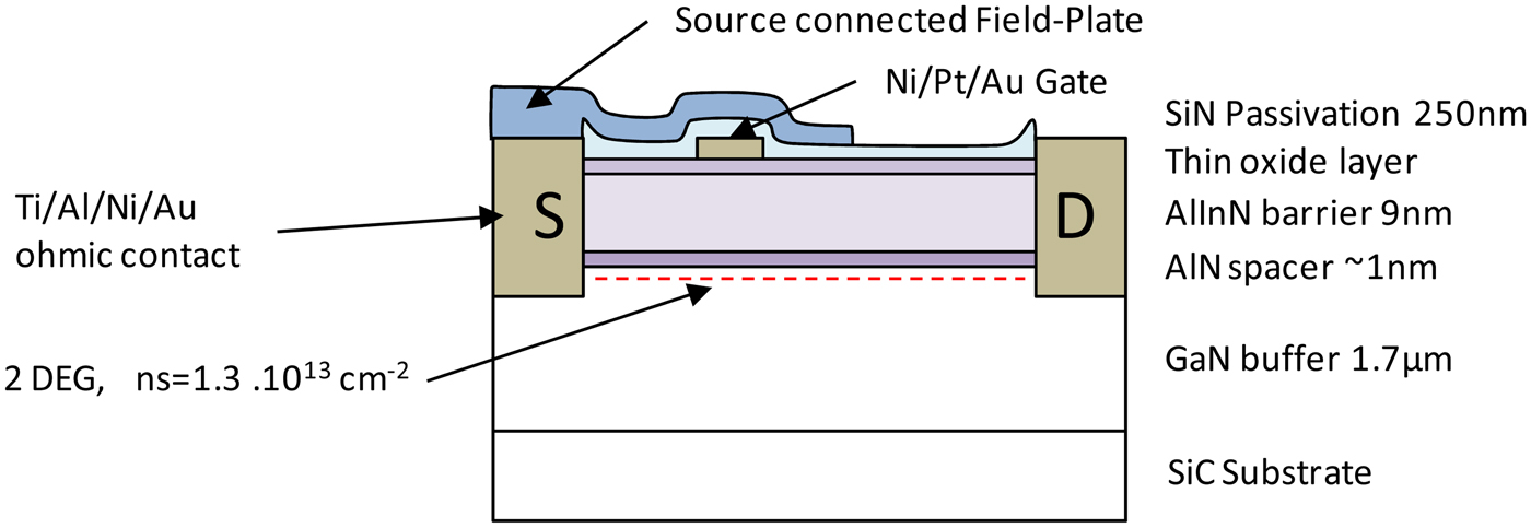
Fig. 1. Schematized cross-section of an InAlN/GaN device processed as detailed in Section II.
III. UNIT CELL ELECTRICAL PERFORMANCES
Pulsed-IV characteristics measurements (pulse length 900 ns, period 1 ms) were conducted on a 6 × 400 × 0.7 µm device, which corresponds to the unit cell of the power bars used in the amplifiers. Different quiescent bias points were chosen, in order to evaluate the gate- and drain-lag-induced current dispersions. Measurements are presented in Fig. 2. The output current, which could be obtained at an optimum radio frequency (RF) load cycle is approximately 1.85 A (0.8 A/mm), and the knee voltage 7.5 V, for a quiescent bias point (V gsq = −3 V, V dsq = 40 V). The RF power slump due to gate-lag effects is estimated at around 11%, and the RF power slump due to drain-lag effects at V dsq = 40 V is estimated at around 7%.

Fig. 2. Pulsed-IV characteristics of an InAlN/GaN 6 × 400 µm HEMT, for different quiescent bias points. In red (V gsq = 0 V, V dsq = 0 V), in green (V gsq = −3 V, V dsq = 0 V), in light blue (V gsq = −3 V, V dsq = 25 V); in dark blue (V gsq = −3 V, V dsq = 40 V). V gsi is stepped from −3 to +1 V.
Small-signal measurements were performed on 2 × 100 × 0.7 and 6 × 400 × 0.7 µm transistors. Biased at V ds = 20 V and I ds = 40 mA (200 mA/mm), 2 × 100 × 0.7 µm devices have a maximum stable gain (MSG) of 23 dB at 2 GHz, a maximum oscillation frequency of 38 GHz, and a transition frequency of 13 GHz. Biased at V ds = 20 V and I ds = 200 mA/mm, 6 × 400 × 0.7 µm devices have a maximum available gain (MAG) of 20 dB at 2 GHz, the MSG/MAG transition occurring at 1.5 GHz, as shown in Fig. 3.

Fig. 3. Maximum oscillation frequency (F max ) and transition frequency (F t ) of a 6 × 400 × 0.7 µm device measured at V ds = 20 V, I ds = 200 mA/mm.
Cw load/pull characterizations were performed on 6 × 400 × 0.7 µm transistors at a fundamental frequency of 2 GHz, harmonic 2 and 3 load impedances being 50 Ω. The bias point was V ds = 40 V and I ds = 100 mA/mm. The devices delivered, on the optimum fundamental load found (|Γ load | = 0.52; φ = 88°), an output power of 10.5 W (4.3 W/mm) with an associated power gain of 16.2 dB, and a Power Added Efficiency (PAE) of 53%, as shown in Fig. 4.

Fig. 4. Power performances of a 6 × 400 × 0.7 µm transistor measured in cw RF at a dc bias V ds = 40 V, I ds = 100 mA/mm, on the optimum fundamental load |Γ load | = 0.52; φ = 88°, harmonic frequencies 2 and 3 being loaded at 50 Ω.
Dc life tests have also been performed for 3000 h on eight 2 × 250 × 0.7 µm transistors, at three different room temperatures: 50, 100, and 150°C. Devices were biased at V ds = 25 V and I ds = 417 mA/mm corresponding to junction temperatures, calculated from three-dimensional (3D) thermal simulations, of 220, 290, and 370°C, respectively. The variations of the current I ds at V gs = +2 V, V ds = 8 V, noted I ds + , were monitored versus time, as shown in Fig. 5. In the three cases, the decrease of approximately 15% of I ds + in the first hours can be attributed to both the “burn-in” of these virgin devices and to trapping effects. This first decrease of drain current can be clearly seen on the inset graph in Fig. 5, where the I–V characteristic evolutions of a sample tested at 370°C are displayed. These I–V characteristics were measured at V gs = 2 V and at different read-out in the test: the main change of the characteristics, especially the drain current and the ON-state resistance occurred mainly during the first half of an hour step of the test.
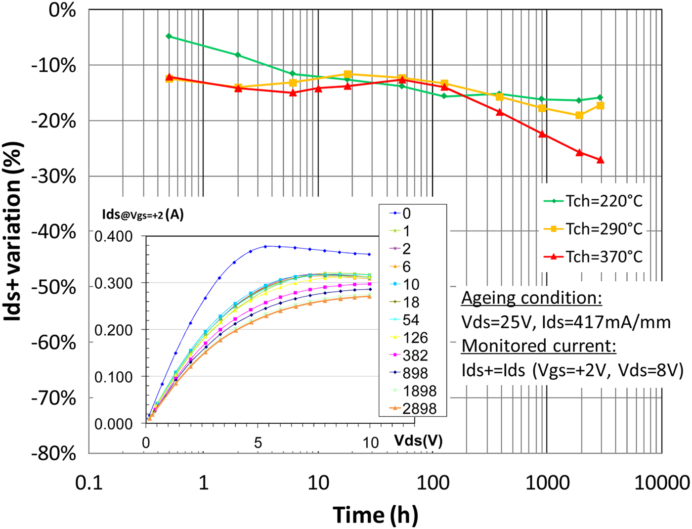
Fig. 5. Results of the ageing tests of eight samples at three different conditions of junction temperatures: 220, 290, and 370°C. The main graph shows the evolution of I ds + (i.e. I ds at V gs = +2 V, V ds = 8 V) versus time. The inset graph shows the evolution versus time (in hours) of the I–V characteristic at V gs = +2 V of a sample aged in the most constraining condition, i.e. T j = 370°C.
Then, the drain current decrease is limited in a 5% range until 500 h for the highest temperature (T j = 370°C) and at least 3000 h for the two other conditions, showing the very low thermal activation of the degradation process in this range of temperatures. However, devices tested at a junction temperature of 370°C experience a faster degradation mechanism after 200 h. This let us conclude on the good capability of such devices to work safely at temperatures as high as 290°C.
IV. AMPLIFIERS REALIZATIONS AND MEASUREMENTS
A) Design and realization
A non-linear model of the 6 × 400 × 0.7 µm transistor was extracted using the model described in [Reference Jardel23]. The power die (15 × 6 × 400 × 0.7 µm) model consists of 15 transistors models wired in parallel with lines, following the geometrical aspects of its layout. 10 Ω balancing resistors, – this value has been determined from previous run experiences –, placed between each drain access pad to prevent odd-mode oscillations, are also taken into account as they may have an influence on the stability simulation results.
The aim of this study was to realize L-band packaged hybrid amplifiers, for operation at 2 GHz, both in the cw- and in pulsed modes. The power dies matching circuits were realized using metalized high dielectric constant ceramics (k = 36 and 80) and controlled bond wire lengths, in order to obtain 50–50 Ω packaged amplifiers. Owing to the impossibility we had to realize line drawings on the high-K ceramics at that time, ceramics pieces with fully metalized surfaces, with length and width chosen for matching purposes, had to be considered. This was not convenient and prevented us to perform harmonic matching. Therefore, conventional class AB or B amplifiers are designed, which could be optimized in PAE if care was taken to harmonic matching. Prior to amplifier design and in order to calibrate our simulations, dummy circuits were realized with such high-K ceramics, wire bonds and 6 × 400 × 0.7 µm transistors for the active circuits. The package, having internal dimensions of 1.3 × 1.5 cm2, was simply modeled considering two independent accesses consisting in lead frames on alumina. The air gap between the package and the external substrate was also considered.
The first version of power amplifier contains one matched power bar; the second one contains two of them. The input and output combiners on the latter, located in the package, are realized on alumina substrates. A photograph of each mounting is shown in Fig. 6.

Fig. 6. Photograph of both version of amplifiers. On the left, with one 36 mm gate development power bar; on the right, with two 36 mm power bars. The diamond heat spreaders can be seen underneath the power dies.
From harmonic balance power simulations, the one-die amplifier is expected to deliver, at V ds = 30 V and in class-AB (I ds = 1.5 A), an output power of 85 W, a PAE of 43%, and a power gain of 10 dB, at the point corresponding to the maximum of PAE. In the same bias conditions (V ds = 30 V, I ds = 2 × 1.5 A), the two-die in package amplifier is expected to deliver an output power of 180 W, a PAE of 42%, and a power gain of 10.1 dB, at the point corresponding to the maximum of PAE. However, the precision of such simulation results may suffer from the fact that transistor models are not electrothermal, even if they have been extracted in order to fit the device power performances obtained in cw conditions. This approximation may result in lower performances of the amplifiers measured in cw conditions, particularly concerning the output power and the PAE.
In order to optimize the thermal management, the power dies were thinned down to 100 µm to avoid the heat flux to reach the edges of the die. Moreover, each die was soldered on a synthetic diamond heat spreader. The material and dimension of the heat spreader (2.6 × 6 × 0.254 mm) were optimized using 3D-finite-element thermal software to maximize the heat transfer between the chip and the package. A very high thermal conductivity (1800 W/m/K) CVD diamond was selected to spread the heat before being transferred to the power package. To maximize the heat transfer at the most critical interface, the top side of the heat spreader is platted with a very thin gold–tin (AuSn) layer (3 µm) allowing a soldering of the power die at the eutectic temperature near 280°C. X-ray imaging was realized to check the quality of the attachment and the absence of void below the active region of the devices. To attach the bottom side to the package, a lower temperature solder was more conventionally used (25 µm – InPb). The package thermal conductivity is also high (400 W/m/K) in order to improve the thermal management of the whole stack-up.
The diamond heat spreader, placed underneath the power bar, allows, thanks to its very high thermal conductivity, to improve the thermal dissipation. Simulations using a 3D-finite-element thermal simulator showed that the insertion of the diamond layer and the additional 3 µm AuSn interface in the whole stack-up contributes to increase its thermal resistance by about 4%. Nevertheless, the large dimensions of this diamond allow a very good spreading of the heat and finally induces a decrease of its total value. Figure 7 shows the total thermal resistance of the package that steps down from 0.84°C/W without heat spreader to 0.56°C/W with a 2.6 mm large diamond heat spreader.

Fig. 7. Evaluation of the total thermal resistance in function of the diamond heat spreader width. The black line corresponds to the thermal resistance without this heat spreader.
Thermal infrared spectroscopy measurements [Reference Carisetti24] were realized on single die amplifiers to confirm the simulations and the interest of the diamond heat spreader. Two amplifiers were compared. The first one represents the nominal version: thinned SiC down to 100 µm and heat spreader, whereas the other version consists in using an un-thinned power die of 400 µm without heat spreader. The amplifiers were biased in dc, in order to dissipate a power of 3.5 W/mm, i.e. 126 W. In the nominal case, the maximum temperature reaches 173°C in the active area (at a room temperature of 25°C), in the second case, it reaches 214°C, as shown in Fig. 8. This difference of 40°C shows the interest of our assembly scheme. The use of an un-thinned power die was necessary for assembly constraints in the amplifier version without heat spreader, due to differences in height. This also contributes to the increase of the temperature. Indeed, 3D thermal simulations showed that on the 40°C improvement, 25°C are related to the use to the diamond and 15°C are related to the thinning of the SiC die.

Fig. 8. Infrared measurements results for two versions of die mounting. On the left, the 36 mm die is soldered on a diamond heat spreader; on the right, it is directly attached on the package. In both cases, the dc bias applied induces a dissipated power of 3.5 W/mm. The thermally optimized version with the diamond heat spreader enables a temperature decrease of 40°C at the hottest spot.
B) Amplifiers measurements
First single-power die amplifiers were measured. Measurement results are presented in Fig. 9. The measurements were performed at 2 GHz, in cw and for a class B bias point at V ds = 30 V. The amplifier delivered 85 W at the point where the PAE reaches its maximum (36%), with a power gain of 10.3 dB [Reference Piotrowicz21]. In this case, the dissipated power was about 140 W (3.9 W/mm), thus a junction temperature of 200°C was calculated (at a room temperature of 30°C). The measurements were pushed up, without any observed fast device degradation, to an output power of 105 W, with an associated PAE of 33%, and a power gain of 8 dB. In this case, the dissipated power was about 175 W (4.9 W/mm), and the junction temperature was estimated to 250°C.

Fig. 9. Power measurements results (Pout, Gain, PAE) of a single-die amplifier measured at 2 GHz, in cw conditions at V ds = 30 V in class-B.
In the RF-pulsed mode (10 µs/10%) at V ds = 30 V in class-B, the amplifier delivered 140 W with 40% of PAE and an associated gain of 10.5 dB. Other measurements were performed at a drain bias voltage of 40 V, in class-B. In these conditions, the output power reached 183 W with 33% of PAE with an associated gain of 10.4 dB. Measurement results are presented in Fig. 10.

Fig. 10. Power measurements results (Pout, Gain, PAE) of a single-die amplifier measured at 2 GHz, in pulsed RF conditions (10 µs, 10%) at a in class-B dc drain bias: V ds = 30 V on the left graph and V ds = 40 V on the right graph.
Amplifiers with two power dies (72 mm total gate width development) mounted in one package were also measured, but only in the pulsed mode, as cw conditions are non-viable for such amplifiers due to the impossibility to correctly manage their self-heating.
For the same reasons, the bias voltage was limited to V ds = 35 V, in class-B. In these conditions, the output power reached 260 W, with a PAE of 34% and a power gain of 9.6 dB (cf Fig. 11).
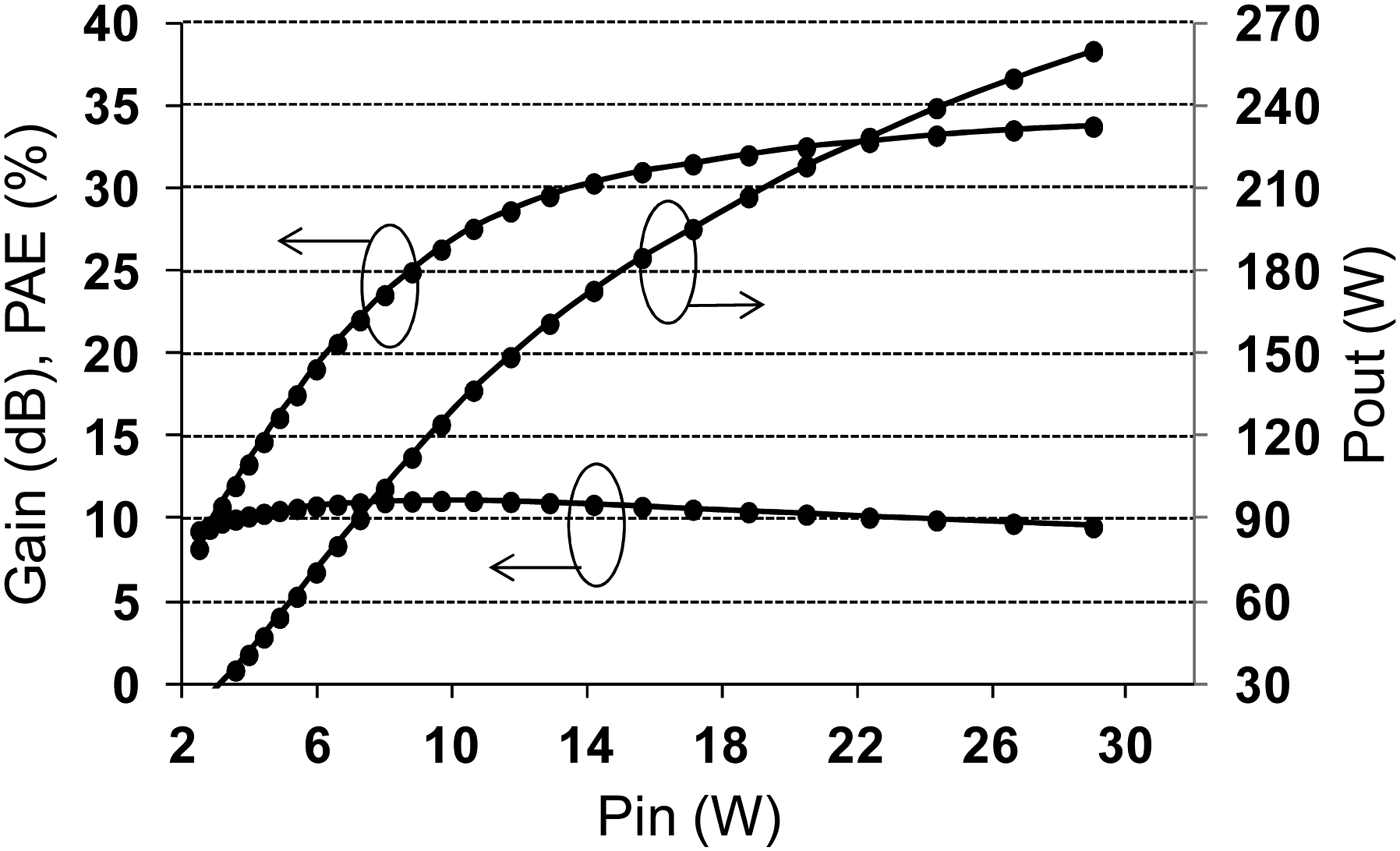
Fig. 11. Power measurements results (Pout, Gain, PAE) of a two-die amplifier measured at 2 GHz, for pulsed RF conditions (10 µs, 10%) at a dc drain bias V ds = 35 V, in class-B. Cw measurements were not possible on this version, for thermal management considerations.
Quite similar performances were obtained in the pulsed mode by measuring a balanced amplifier composed by two single power die. An output power of 240 W was obtained, with a PAE of 34% and a power gain of 10 dB, for a class-B gate quiescent biasing point at V ds = 30 V. However, the better thermal management offered by using two single die packaged amplifiers compared to the previous solution with one double die packaged amplifier allowed us to perform measurements in class AB at V ds = 30 V and I ds = 2 × 1.5 A, leading to an output power of 260 W, with a PAE of 37% and a power gain of 10.2 dB. Cw measurements were also carried out in class B at V ds = 30 V, showing an output power of 180 W, a PAE of 31% and a power gain of 8.4 dB (at 2 dB gain compression). No fast ageing of the amplifiers was noticed after repetitive measurements in the conditions previously enounced. These results are presented in Fig. 12, beside a photograph of the amplifier.

Fig. 12. Photograph of a single die balanced amplifier, on the left. On the right, power measurements results (Pout, Gain, PAE) at 2 GHz, for pulsed RF conditions (10 µs, 10%) at a dc drain bias V ds = 30 V, in class-B (triangles – medium gray), for pulsed RF conditions at a dc drain bias V ds = 30 V in class AB (I ds = 2 × 1.5 A) (squares – light gray), and for cw RF conditions in class-B at a drain bias V ds = 30 V (circles – black).
V. CONCLUSIONS
The realization of L-band power amplifiers using InAlN/GaN HEMT technology was presented. If the amplifiers deserve improvements concerning the PAE, for instance by harmonic matching, in order to decrease the temperature and make this technology more competitive with the more classical AlGaN/GaN HEMTs, different versions were presented and show the interest of such technology to deliver very high power and to maintain high-power densities on large periphery devices, in this frequency band. Besides, the single-die amplifier delivers an output power of 183 W in the pulsed mode biased at 40 V and the double-die amplifier allows us to reach output powers over 250 W, for the very first time using this new InAnN/GaN structure. Finally, the interest of diamond heat spreaders for better thermal management is also demonstrated, as well as the capability of the transistors to work without fast degradation at temperatures as high as 290°C.
ACKNOWLEDGEMENT
This work was supported by the EU under project “MORGAN” FP7/2007-2011 no. 214610.
 Olivier Jardel received the Engineer degree from the University of Aix-Marseille I, in 2004, and the Ph.D. degree from the University of Limoges in 2008, in the common laboratory MITIC between XLIM and III–V Lab. Since 2008, he is a research engineer at III–V Lab and is involved in the development of GaN HEMT power devices. He is in charge of electrical characterizations, transistor modeling, and circuit design.
 Jean-Claude Jacquet received the Engineer degree from the Ecole Supérieure d'Optique, Orsay, France, in 1990. He subsequently joined the Central Research Laboratory of Thales, as a Research Staff Member, where he was involved with spintronic devices. He focused his efforts on the giant magnetoresistive effect and found a new physical effect called the magnetorefractive effect. Since 1999, he has been involved in the development of GaInP HBT and GaN HEMT microwave power devices. He is currently in charge of the thermal management and of the physical modeling aspects of GaN HEMTs at III–V Lab.
 Lény Baczkowski received the Diploma of Engineer degree from the University of Lille 1 (Polytech' Lille), France, in 2012. He is currently working toward the Ph.D. degree at the Institute of Electronic, Microelectronic, and Nanotechnology (IEMN), University of Lille (in collaboration with Thales Airborne Systems, Elancourt, Thales Research and Technology, Palaiseau, and III–V Lab, Marcoussis, France). His research interests are dedicated to thermal simulations and characterizations of power amplifier for radar applications.
 Maxime Olivier received Master's degree in Electronic and Microwave Engineering from the University of Lille, in 2007. He is currently working in the development department of Thales Air Systems, Rouen-Ymare, France, and is in charge of design and characterization of hybrid amplifiers, limiters, and MMIC circuits for T/R modules.
 Raphaël Aubry received the Material Engineering degree from ECAM Rennes in 1999, the Physic master research degree from University of Rennes in 2000 and Ph.D. degree from University of Lille in 2004. His Ph.D. work subject was on the thermal management of the power microwave devices. He joined the THALES Research Center and has been working on the development of the power AlGaN/GaN HEMT technology for radar and space applications. He is currently at III–V Lab, and in charge of the process of GaN-based devices.
 Marie-Antoinette di Forte Poisson was graduated from Ecole Nationale Supérieure of Physique (Marseille) in 1976 and completed her Ph.D. degree in optics at the University of Nice in 1978. She joined in 1978 the Central Research Laboratory of Thomson-CSF and achieved an MBA at IAE, University of Paris, in 1979. She is involved in the MOVPE epitaxy of III–V compounds. She has authored or co-authored more than 100 papers and several patents. She obtained in 1997 and 2002 two Thales awards. She currently manages “Epitaxial Growth of Wide Band-gap Materials” team at III–V Lab. She successfully co-ordinated the Brite-Euram project RAINBOW (Gallium–Aluminum–Indium–Nitride for Multicolor Sources) and other national projects of GaN based and was also involved in many French or European projects. She is a Program Committee Member of the MO-VPE EUROPEAN WORSHOP, the MOVPE International Conference and the International Symposium on Growth on III-Nitrides (ISGN).
 Christian Dua received the Engineer degree in Physics from the University of Clermont-Ferrand, France. He joined THOMSON-CSF Group (previous name of THALES) in 1982. He has been working in two different Units of the Group whose main activities were microwave devices (mainly diodes) and optoelectronic components (lasers and LEDs). During this period he gained experience in crystal growth (using several techniques such as Vapor Phase Epitaxy, Liquid Phase Epitaxy, Metal Organic CVD, and Chemical Beam Epitaxy) and physical and electrical characterizations of Semiconductor epi-layers and substrates. He is presently working in the SiC activity of the research unit, TRT, and is involved in characterization and assessment of the supplied wafers, and in the study of the reliability of the GaN HEMT technology.
 Stéphane Piotrowicz received the Ph.D. degree in Electronics from the University of Lille in 1999. He currently works on the development of GaN technologies at III–V Lab (a joint lab of Alcatel-Lucent Bell Labs France, Thales Research and Technology & CEA Leti). He is in charge of the design and characterization team involved the realization of hybrid and MMIC circuits for T/R modules as power switches, power amplifiers, and low-noise amplifiers.
 Sylvain L. Delage obtained his Ph.D. degree from the University of Paris VII in 1985 for his work on monolithic Si/CoSi2/Si Metal Base Transistor grown by MBE. Afterwards he was for 2 years with IBM T.J. Watson Research Center as research staff member, where he participated to the first demonstration of Si/SiGe HBTs. In 1988, he joined the Central Research Laboratory of Thomson-CSF, where he was in charge of the Power Transistor Program for Microwave Applications. This work gave rise to the demonstration of InGaP/GaAs HBT devices and microwave circuits. He is now working at III–V Lab, in charge of the Microelectronics Group, which includes 25 permanent scientists working on GaN and InP materials and devices. Sylvain Delage was formerly Member of the French National Committee of Research and a member of the Technical Program Committee of the EuMIC Conference. He contributed to more than 100 publications and 25 patents.


