Introduction
There has been increased interest in frequency agile front-end components for millimeter (mm)-wave communication networks [Reference Entesari, Saghati, Sekar and Armendariz1], as they provide flexibility to select different frequency bands using the same infrastructure through post-fabrication tuning methods [Reference Entesari, Saghati, Sekar and Armendariz1]. Substrate-integrated waveguide (SIW) [Reference Bozzi, Georgiadis and Wu2] frequency agile circuits have been demonstrated [Reference Sirci, Martinez, Taroncher and Boria3–Reference Anand, Small, Peroulis and Liu5] but requires DC-isolated planes for varactor biasing [Reference Eccleston6]. As a result, multiple etched annular rings [Reference Anand, Small, Peroulis and Liu5] and bridging wires [Reference Sirci, Martinez, Taroncher and Boria3, Reference Sirci, Martinez, Taroncher and Boria4] are required for biasing, with or without additional floating pads [Reference Anand, Small, Peroulis and Liu5] that require connection through wire leads.
Planar groove gap waveguide (PGGWG) [Reference Oyedokun, Geschke and Stander7] features propagation characteristics similar to groove gap waveguide (GGWG [Reference Berenguer, Fusco, Zelenchuk, Sánchez-Escuderos, Baquero-Escudero and Boria-Esbert8]) in a planar printed circuit board (PCB) process similar to what is used for SIW. Unlike SIW, however, it provides the benefit of DC-isolated conducting planes, which may be exploited for easy varactor biasing without the need for bridging wires as used in e.g. [Reference Sirci, Martinez, Taroncher and Boria4]. It has also been shown that the resonant cavity Q-factor of PGGWG is comparable to SIW [Reference Oyedokun, Geschke and Stander7], but that PGGWG exhibits a slow-wave response compared to SIW, which aids in reducing the resonant cavity size [Reference Oyedokun, Geschke and Stander9]. This was previously demonstrated through broadband propagation studies of PGGWG [Reference Oyedokun, Geschke and Stander9] and fixed frequency resonators [Reference Oyedokun, Geschke and Stander7], but has yet to be explored in tunable resonant cavities. The addition of varactor loading across the capacitive gap of the fixed frequency resonator in [Reference Oyedokun, Geschke and Stander7] would make the resonator tunable, but without the need for annular and bridging wires as is commonly required in varactor-loaded SIW tunable cavities.
This paper presents experimental results for a tunable Ka-band (commonly used for satellite communications and 5G base stations [Reference Simon, Schaefer, Bruni, Campo, Litschke, Otto and Holzwarth10], radio astronomy [Reference Sitwala, De Witt, Van den Heever, Malan and Stander11], and cloud liquid water radiometry [Reference Behrens and Stander12]) PGGWG resonant cavity exploiting the DC isolation advantage of the structure, using a simple varactor diode basing scheme previously analyzed theoretically [Reference Oyedokun, Geschke and Stander13, Reference Oyedokun, Geschke and Stander14]. We extend on the prior simulation study by presenting a detailed circuit-electromagnetic (EM) co-simulation model, providing measurement results, investigating discrepancies between simulated and measured results through a detailed inspection of the multi-layer PCB stack-up (providing critical data for improved first-iteration modeling and prototyping accuracy for PGGWG development in future, which is not reported in [Reference Oyedokun, Geschke and Stander13, Reference Oyedokun, Geschke and Stander14]), and systematically comparing the measured data to those of other approaches in the state-of-the-art literature.
Tunable PGGWG cavity geometry
PGGWG is realized within parallel plate waveguide by using blind vias and catch pads to create an electromagnetic bandgap (EBG) medium on either sides of a groove (Fig. 1(a)) [Reference Oyedokun, Geschke and Stander7]. The groove allows for the propagation of TE10 mode similar to that in SIW. The EBG suppresses the parallel plate mode that would otherwise propagate along the sidewalls, similar to machined GGWG [Reference Rajo-Iglesias and Kildal15]. The advantage of biasing varactors using PGGWG is evident by the comparison in Figs 1(b) and 1(c). Although a varactor-loaded combline cavity in PGGWG may be loaded using only conventional surface-mount components and etched DC traces, the loading of varactors in coaxial SIW cavities requires a bridging wire and multiple annular rings. It is the bridging wires, in particular, that hamper mass production of the circuit, as it is a manufacturing step incompatible with automated pick-and-place PCB assembly. The disadvantage of PGGWG is that at least three copper routing layers are required, while SIW may be implemented on a single double-sided PCB. However, as multi-layer PCBs are commonly used for e.g. SatCom applications [Reference Simon, Schaefer, Bruni, Campo, Litschke, Otto and Holzwarth10], this is not necessarily a major drawback to the topology.

Fig. 1. (a) PGGWG cavity cross-section. (b) RF and DC signal path in PGGWG rectangular resonant cavity. (c) RF and DC signal path in SIW resonant cavity [Reference Sirci, Martinez, Taroncher and Boria4].
The geometry of the rectangular tunable PGGWG cavity described here resembles a combline resonator topology, although the field pattern suggests a TE101 operating mode. The rectangular resonant cavity shown in Fig. 2 uses three rows of EBG vias to form cavity sidewalls. This has been demonstrated to be sufficient to suppress parallel waves, ensuring that the field is confined within the groove [Reference Oyedokun, Geschke and Stander7]. The dimensions of the cavity are shown in Table 1. The non-PTFE, low-cost Mercurywave 9350 substrate with ɛr = 3.5 and loss tangent of 0.004 was used.
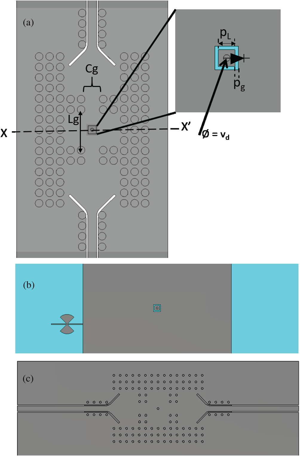
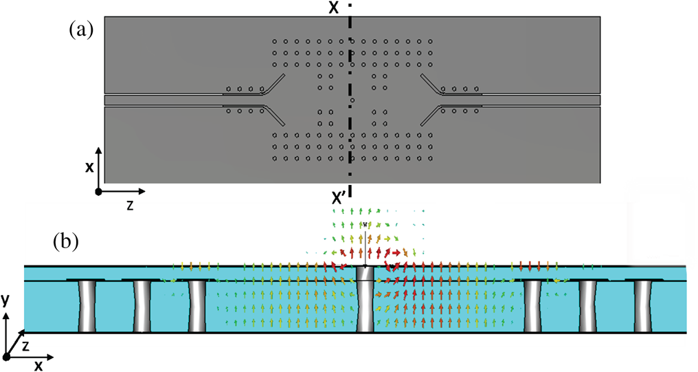
Fig. 2. PGGWG rectangular resonant cavity structure. (a) Inside view of the cavity. (b) Top view showing the center via and isolated metal patch and varactor diode attachment. (c) Bottom view.
Table 1. Dimensions of the tunable PGGWG rectangular resonant cavity

The length of the cavity, Lg is chosen to ensure the fundamental TE101 mode resonates in the cavity while the coupling to the cavity, set by the iris width Cg, is chosen to minimize port loading effects, as is required by the three-point Q 0 extraction method [Reference Leong and Mazierska16]. The application of this technique requires light coupling (as seen in e.g. Fig. 5) and values of S 11 ≈ 1, leading to the approximation of Q 0 ≈ Qe in extracting Q 0 from S-parameters. A through-hole plated via of diameter vd = 0.3 mm is placed at the center of the cavity connecting the top isolated patch with the bottom conducting plane. The etched gap of width pg ensures DC isolation despite the through-hole via in the middle of the cavity. The gap creates a capacitive loading between the center post and the top metal layer of the PGGWG through the fringing fields across the gap. This can be observed in Fig. 3 in the gap between the island patch and the top metal plate. As there is no experimentally defined definition of effective cavity width for PGGWG (as is available for SIW [Reference Caranicola and Fatima Salete17]), and since the analytically-defined coaxial resonant mode in [Reference Sirci, Martinez, Taroncher and Boria3] is not present here, the cavities are sized using full-wave parameter tuning.

Fig. 3. Electric field vector plot inside the cavity.
Extensive parametric studies on the effects of p, h, vd, and ha variation on PGGWG have been presented previously [Reference Oyedokun, Geschke and Stander9, Reference Oyedokun, Geschke and Stander13]. The results of these parametric studies are applied here, to ensure that the band gap generated by the blind via rows (which effectively form the cavity sidewalls) covers the frequency range of the loaded TE101 resonant mode of the cavity, as determined by Lg (selected to be approximately λg/2 at the required f 0, given the value of β reported in [Reference Oyedokun, Geschke and Stander9]) and w.
A sequential multilayer PCB build is applied in the manufacturing of the PGGWG. The EBG via holes are first drilled and plated on the substrate of height h, followed by through-hole plating and etching of the catch pads from the 17.5 μm copper cladding. The top substrate layer ha is then added. The center via of the cavity is then drilled through the stack-up and through-hole plated, after which the floating pad is etched. As the center via is only drilled and plated after lamination, there is no risk for misalignment of separately drilled and plated vias (which may have been the case if the h and ha substrates were drilled and plated separately prior to lamination). Consequently, there is no need for a catch-pad to provide for possible misalignment in the center via.
Simulation results
The loading capacitance Cg across the gap pg of Fig. 2 is controlled electrically by placing a varactor diode in reverse bias across the gap [Reference Oyedokun, Geschke and Stander13]. The varactor diode is biased by applying the DC voltage directly to the top conducting plane via a butterfly stub, which presents an RF open circuit at the point of contact with the top plate of the PGGWG cavity and an RF short circuit at the DC side of the stub.
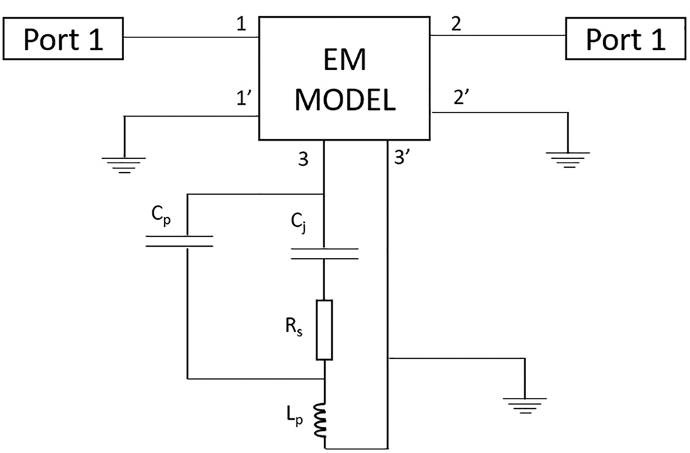
An EM-circuit co-simulation is performed in CST Microwave Studio using the time domain solver as shown in Fig. 4. A MACOM 46580 varactor diode is selected in this design example, with Cjo = 1.57 pF. The parasitics of the varactor diode packaging, Cp and Lp are also included, as detailed in the manufacturer's datasheet.

Fig. 4. 3D EM-circuit co-simulation set-up showing the equivalent circuit model for MACOM 46461-276 varactor diode connected.
Figure 5 shows the resulting S-parameters, which indicates a variation of f 0 from 31.63 to 32.71 GHz (3.36% tuning range) achieved by varying the junction capacitance from 0.15 to 0.45 pF. Neglecting surface roughness, the unloaded Q-factor varies over the tuning range from 143 to 160. In addition to the effect of parametric variations on h, vd, and pd reported previously [Reference Oyedokun, Geschke and Stander7–Reference Oyedokun, Geschke and Stander9], the parametric sweeps shown in Figs 6 and 7 indicate that the resonant frequency of the PGGWG cavity could be selected from a combination of parameters. In Fig. 6, it can be observed that an increase in the width w (parameter indicated in Fig. 1) decreases the resonant frequency of the cavity. Similarly, the changes in the cavity length Lg as shown in Fig. 7 influence the resonant frequency of the cavity. The inverse relationship between f 0 and w, as well as Lg, supports the view that the cavity exhibits a TE101-type resonant mode, although the effective width aeff is not well-defined as with SIW, which complicates an analytical calculation of f 0.
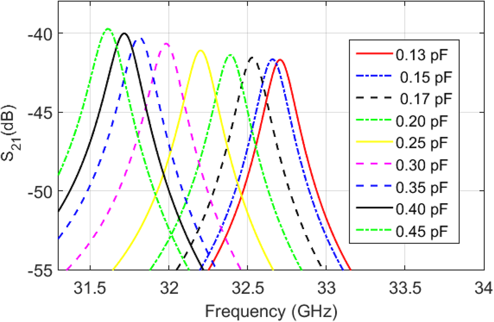
Fig. 5. EM co-simulation result of S 21 (dB) of the two-port loaded rectangular PGGWG cavity.
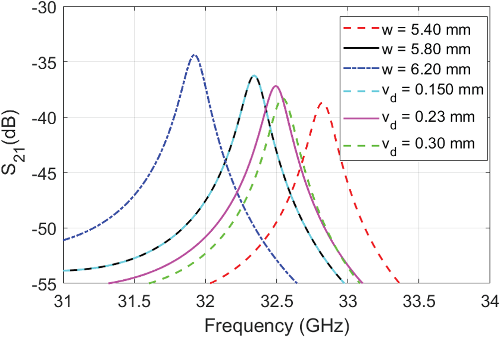
Fig. 6. Parameter sweep of tunable PGGWG cavity dimensions for a constant varactor Cj = 0.37 pF. Variation in w and vd is shown.

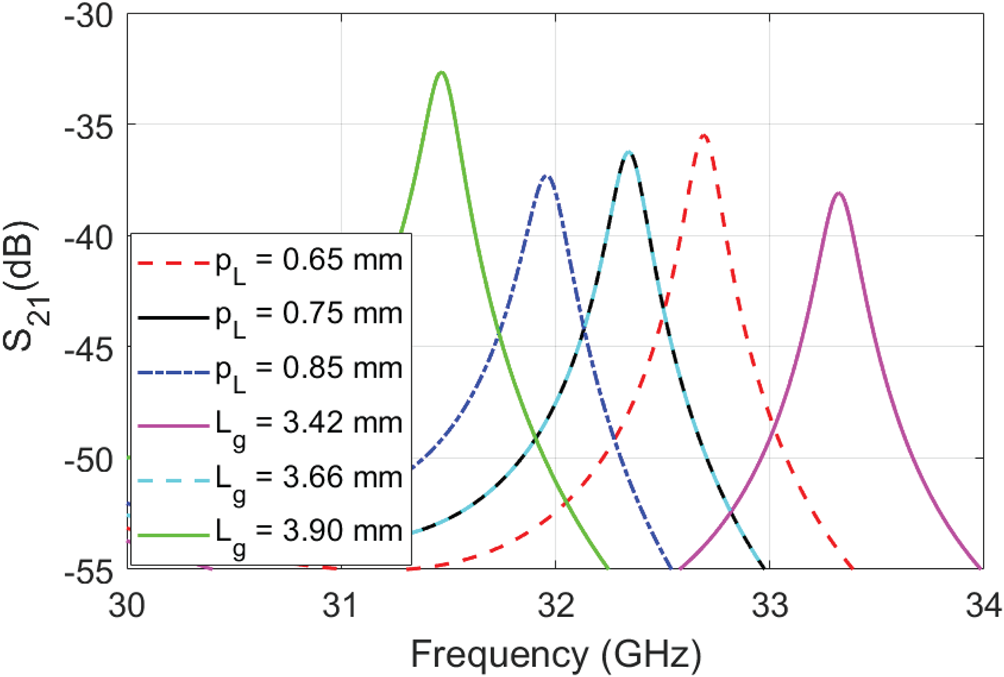
Fig. 7. Parameter sweep of tunable PGGWG cavity dimensions for a constant varactor Cj = 0.37 pF. Variation in p L and L g is shown.
A variation in the square catch pad dimension, pL is shown in Fig. 7. A larger pad results in lower resonant frequency, due to an increased capacitive load to the PGGWG cavity. In comparison, variation in the via diameter, vd, has a much smaller effect on resonant frequency, as shown in Fig. 6.
Construction and measurement results
Figures 8(a) and 8(b) show the fabricated circuit (top and bottom views) with the varactor diode attached. Micrographs of sectioned views along the sidewall X 1–X 1′ and along the center X–X′ are shown in (Figs 8(c) and 8(d)), respectively.
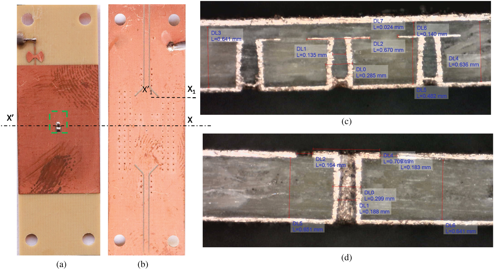
Fig. 8. Photographs of the fabricated PGGWG tunable cavity circuit. (a) Top view with varactor diode attached. (b) Bottom view. (c) Micrographs showing the cross section X 1–X 1′. (d) Micrographs showing the cross section X–X′. (e) Varactor diode attachment on the top plane. (f) DC bias line.
The prototype is characterized on an Anritsu MS4647A VNA (Fig. 9). The measured results shown in Fig. 10 indicate a 4.48% continuous frequency tuning range from 32.52 to 33.98 GHz, corresponding to DC bias voltage range of 0–16 V. The resonator Q 0 varies from 63 to 85 across the tuning range. Table 3 compares simulated and measured results.

Fig. 9. Photograph of the fabricated circuit attached to the network analyzer.

Fig. 10. Measured S 21 (dB) of the tunable PGGWG cavity.
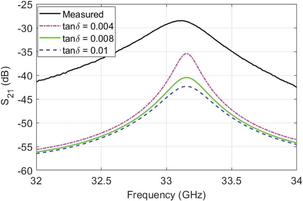
After including 1.6 μm RMS copper foil surface roughness [Reference Liang, Hall, Heck and Brist18] in the EM co-simulation of the tunable cavity, the discrepancy between simulated and measured Q-factors can be replicated, in simulation, by increasing RS to 2.0 Ω (100% increase) resulting in an unloaded Q-factor of 76, or increasing tan δ to 0.01 (150% increase) with unloaded Q-factor of 87. These changes can be observed in Figs 11 and 12. The cause for the reduced Q-factor is, therefore, more likely to be underestimation of RS in the circuit model than underestimation of tan δ.
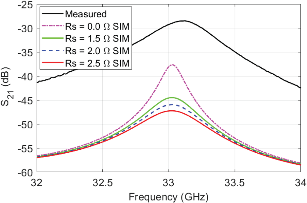
Fig. 11. Comparison for Rs and tan δ with surface roughness 1.6 μm included in EM-co simulation of the tunable cavity. Rs is varied with Cjo = 0.37 pF, tan δ = 0.004.

Fig. 12. Comparison for Rs and tan δ with surface roughness 1.6 μm included in EM-co simulation of the tunable cavity. tan δ is varied with Rs = 1.0 Ω, Cjo = 0.37 pF.
The discrepancy between the simulated and manufactured geometries, as determined by the micrograph, is shown in Table 2. This manufacturing error can explain the shift in the resonant frequency of the circuit. A variation in the catch pad size pd changes the resonance frequency of the cavity [Reference Oyedokun, Geschke and Stander9]. A decrease in the pad dimension increases the suppression band of the EBG, therefore increasing the resonant frequency of the cavity. Also, as observed in Table 3, the gap height ha indicates a manufacturing error of 28 μm (16.6%). This changes the capacitance between the top conducting plane and the round catch pad, resulting in a shift of the suppression band of the PGGWG structure. Furthermore, the shift in frequency can also be attributed to an underestimation of the varactor parasitics in simulation. The 12 dB discrepancy between simulated and measured S 21 maxima represents a variation of only 2.4% in transmission magnitude, and may safely be attributed to increased strength in coupling resulting from the reduced values of pd and vd. The three-point Q 0 characterization method [Reference Leong and Mazierska16] is not affected by this discrepancy, although this variation should be carefully considered in other applications where a specific Qe is sought (e.g. in filter or voltage controlled oscillator (VCO) circuits).
Table 2. Comparison between the dimensions of simulated and fabricated circuits
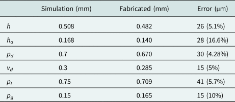
Table 3. Comparison between simulated and measured results
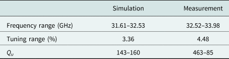
Table 4 compares our study to the state-of-the-art research studies in terms of achieved f 0, Q 0, tuning range, number of varactors used, and the necessity for bridging wires or multi-layer routing. S-parameters and external Q-factor Qe are omitted from the comparison, as these are functions of resonator coupling (as determined by the synthesis of the application filter or VCO) and are not intrinsic performance metrics of the resonator itself [Reference Leong and Mazierska16]. From this table, it is evident that to enable varactor diode biasing, state-of-the-art schemes require multi-layer routing or bridging wires bridging wires or multi-layer routing, to which this study is an exception.
Table 4. Comparison of tunable resonant cavities

Conclusion
Experimental validation of a tunable PGGWG resonant cavity is presented. This prototype demonstrates the benefit of PGGWG over SIW by exploiting the DC-isolated conducting planes to bias a varactor diode, without annular rings or bridging wires to create a frequency agile combline resonator. Future research will extend this approach to other frequency agile applications, such as tunable filters and VCOs, establish analytical methods to synthesize the cavity, as well as experimental comparison with other planar guided media with similarly DC-isolated planes, e.g. corrugated SIW [Reference Eccleston6].
Acknowledgement
This study was supported in part by the National Research Foundation of South Africa (Scholarship 99870 and Grant number 88100).
 Titus Oyedokun received his B.Sc., M.Sc., and Ph.D. in Electrical Engineering from the University of Cape Town, South Africa, in 2009, 2012, and 2019, respectively. In 2018, he joined Max Planck Institute for Radio Astronomy in Bonn Germany working as a research scientist on the development of cryogenic phased array feeds for radio telescope. His research focus is on planar waveguide technologies used in front-end radio receivers.
 Riana H. Geschke's Ph.D. research was on the topic of hybrid methods for computational electromagnetics. She was previously an Associate Professor at the University of Cape Town in South Africa, where her research activities were focused on the field of applied electromagnetics and radio astronomy systems. Since March 2019, she is a Research Scientist with the Fraunhofer Institute for High Frequency Physics and Radar Techniques (FHR) in Wachtberg, Germany.
 Tinus Stander received his B.Eng. and Ph.D. degrees in Electronic Engineering from the University of Stellenbosch, Stellenbosch, South Africa, in 2005 and 2009, respectively. From 2010 to 2012, he served as an RF and Microwave Engineer at Denel Dynamics (a division of Denel SOC, Ltd.). He joined the Department of Electrical, Electronic, and Computer Engineering, Carl and Emily Fuchs Institute for Microelectronics, University of Pretoria, in 2013. He currently serves as a Principal Investigator in microwave and millimeter-wave microelectronics at the Institute, with personal research interest in the application of distributed passives on-chip and built-in self-testing. He is also registered as Professional Engineer with the Engineering Council of South Africa and serves as a Scientific Advisor with Multifractal Semiconductors (Pty) Ltd.