


I INTRODUCTION
Modern modulation schemes like wideband code-division multiple access (W-CDMA) have very high requirements concerning the linearity of the power amplifier (PA). Therefore, a variety of efficient PA architectures, for example, class B–F cannot be used due to their nonlinearities. The major drawback of the remaining architectures (classes A and AB) is a very poor efficiency if they operate in back-off. Because of the advanced output power regulation of state-of-the-art communication systems the back-off operation is very likely. Hence, the average efficiency of the PA is very low, which leads to a high-power consumption. This behavior shortens battery operation of the device and therefore limits the mobility of the user.
Several publications demonstrate different approaches to overcome this problem. There are hybrid amplifier configurations like Doherty amplifiers [Reference Yamamoto, Kitahara and Hiura1] and linear amplification with nonlinear components (LINC) [Reference Birafane, El-Asmar, Kouki, Helaoui and Ghannouchi2]. But the on-chip realization of the required power divider and combiner is difficult and very lossy. A class of systems, which is much more attractive for a system-on-chip solution, modulates the supply voltage of the PA. The Kahn envelope elimination and restoration (EER) [Reference Vasić3] technique divides the amplifier input signal in a magnitude and a phase branch. The phase is amplified with a high efficient but nonlinear PA. The envelope of the output signal is adjusted by a DC–DC converter, which is controlled by the magnitude branch and modulates the PA supply voltage. A similar approach creates the magnitude and phase information, which is already in the digital base band and is called polar transmitter [Reference Brain, Paul, Paul, Peter and Mark4]. The envelope following (EF) [Reference Brain, Paul, Paul, Peter and Mark4, Reference Staudinger5] and envelope tracking (ET) [Reference Brain, Paul, Paul, Peter and Mark4, Reference Sahu and Rinćon-Mora6] techniques use linear PAs in class A or AB configuration. By modulating the supply voltage, the amplifier always operates very close to saturation. Thereby, its efficiency significantly increases. Whereas ET only follows slow changes of the input signal envelope caused by changing radio signal propagation conditions, EF also enables fast changes through the modulation.
All these techniques, except ET, have one thing in common: they need an efficient DC–DC converter with a very high bandwidth to follow the fast changing envelope signal. Hence, this work presents a systematic way to handle this challenge. Thereto, an accurate system model has to be developed. It is used to find the optimal configuration of the proposed buck converter. To prove the correctness and the feasibility of the theoretical part, a fully integrated (except for the capacitor and the inductance of the output filter) Complementary Metal Oxide Semiconductor (CMOS) circuit is presented. The measurements, taken on the buck converter and its application in an EF system with a W-CDMA PA, verify the performance of the design and the theoretical considerations.
II SYSTEM CONSIDERATIONS
The basis of the following analysis is the EF system depicted in Fig. 1. A buck converter, controlled by the envelope of the W-CDMA modulated RF input signal, is used to modulate the supply voltage of a PA in class A or AB configuration.

Fig. 1. Simplified diagram of linear power amplifier (PA) combined with the envelope following (EF) technique.
A) Buck converter
The majority of designs uses a pulse-width modulation (PWM) generator in conjunction with a proportional–integral–derivative (PID) controller to control the converter power switches [Reference Mihajlovic, Lehman and Sun7, Reference Pinon, Allard and Garnier8]. The behavior of this approach can be easily characterized by the means of linear control theory. The switching frequency is defined exactly through the fixed period of the PWM signal. But an implementation with a very high bandwidth is difficult due to the complexity of the individual components. Hence, the straightforward and robust sliding mode like control approach shown in Fig. 2 is applied. Its dynamic behavior is characterized by the following nonlinear delayed differential equation (DDE):
 $${\dot x}\lpar t\rpar =\left\{{\matrix{ {A_ - x\lpar t\rpar +b_ - } \hfill & {{\rm for}\; V_{S} \lpar t - \Delta t\rpar +\displaystyle{{\tau I_L } \over C}\lt c^T x\lpar t - \Delta t\rpar }\comma \hfill \cr {A_+x\lpar t\rpar +b_+} \hfill & {{\rm otherwise.}} \hfill}}\right.$$
Fig. 2. Model of the proposed buck converter control architecture.
The vector  $x = \left({\matrix{ V & I \cr } } \right)^T $ denotes the state of the system and consists of the voltage across the capacitor C and the current through the inductor L. The matrices A −, + and the vectors b +,− and c were introduced to present the DDE and also the following equations in a compact form. They are defined as follows:
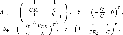 $$\matrix{A_{ -\comma +} = \left({\matrix{ { - \displaystyle{1 \over {CR_L }}} & {\displaystyle{1 \over C}} \cr { - \displaystyle{1 \over L}} & { - \displaystyle{{R_{ -\comma +} } \over L}} \cr } } \right)\comma \quad b_{-} = \left({\matrix{ { - \displaystyle{{I_L } \over C}} & 0 \cr } } \right)^T \comma \hfill \cr b_ +=\left({\matrix{ { - \displaystyle{{I_L } \over C}} & {\displaystyle{{V_{DD} } \over L}} \cr } } \right)^T \comma \quad c=\left({\matrix{ {1 - \displaystyle{\tau \over {CR_L }}} & {\displaystyle{\tau \over C}} \cr } } \right)^T. } \eqno\lpar 2\rpar$$
For a fixed setting of the power switches S an inhomogeneous differential equation describes the propagation of the state vector x. Hence, it is possible to introduce an affine transformation
 $$\eqalignno{&{\cal T}_{\Delta t}^\sigma x = {\it e}^{A_{\sigma} \Delta t} \left(x\lpar t\rpar - x_\sigma \right)+ x_\sigma = x\lpar t + \Delta t\rpar \comma \; \cr & \quad \sigma \in \left\{-\comma \; + \right\}\comma \;}$$
which evaluates the propagation of the space of all state vectors (phase space) for a given time t and the setting σ of S. As A σ is a 2 × 2 matrix, the exponential matrix used in this equation can be calculated in the following way:
 $${e}^{A_\sigma t}={e}^{ - \delta _\sigma t} \left[{1\cos \; \Omega _\sigma t+\displaystyle{{A_\sigma+1\delta _\sigma } \over {\Omega _\sigma }}\sin \; \Omega_\sigma t} \right].\eqno\lpar 4\rpar$$
The variable δσ denotes the real part and Ωσ the positive imaginary part of the two conjugate complex eigenvalues of A σ
 $$\delta_\sigma = \displaystyle{1 \over {2CR_L}} + \displaystyle{{R_\sigma } \over {2L}}\comma \; \quad {\Omega _\sigma} = \sqrt {\displaystyle{1 \over {LC}} \left({1 + \displaystyle{{R_\sigma } \over {R_L }}} \right)- \delta _\sigma ^2 } .\eqno\lpar 5\rpar$$
The stationary state for each setting of the power switches is characterized by the vectors
 $$x_ -=\displaystyle{1 \over {R_L+R_ - }}\left({\matrix{ { - I_{L} R_ - R_{L}} \cr {I_{L} R_{L} } \cr } } \right)\comma \; \eqno\lpar 6\rpar$$
 $$x_ +=\displaystyle{1 \over {R_L+R_+}}\left({\matrix{ {\left[{V_{{DD}} - I_{L} R_+} \right]R_{L}} \cr {V_{{DD}}+I_{L} R_{L} } \cr } } \right).\eqno\lpar 7\rpar$$
Assuming that the input signal V S is continuous, the points in time t K when S are changing their state are specified by the following transcendental nonlinear system of two equations:
 $$\eqalign{&\matrix{ {V_{S} \lpar t_{2k+1} - {\Delta }t\rpar +\displaystyle{{\tau I_L } \over C}=} {c^T {{\cal T}}_{{\Delta }t_{2k} - {\Delta }t}^ - x_{2k}\comma \; }\cr& \hfill \cr {V_{S} \lpar t_{2k+2} - {\Delta }t\rpar +\displaystyle{{\tau I_L } \over C}=} {c^T {{\cal T}}_{{\Delta }t_{2k+1} - {\Delta }t}^+x_{2k+1}}\comma \; \hfill \cr } \cr&{\rm with}\; {\Delta }t_k=t_{k+1} - t_k \; {\rm and}\; x_k=x\lpar t_k \rpar .}\eqno\lpar 8\rpar$$
If there exists more than one solution for t 2k or t 2k+1, the smallest positive one has to be used for further considerations. With the set of n points in time t k and an initial condition x(t 0) the state of the model is determined for all times t 0 < t < t n by a recursive equation as follows:
 $$x\lpar t\rpar = \left\{{\matrix{ {{\rm {\cal T}}_{t - t_{2k} }^ - x_{2k} } \hfill & {{\rm for}\; t_{2k} \leq t \leq t_{2k+1} }\comma \; \hfill \cr {{\rm {\cal T}}_{t - t_{2k+1} }^+x_{2k+1} } \hfill & {{\rm for}\; t_{2k+1}\lt t\lt t_{2k+2}. } \hfill \cr } } \right.\eqno\lpar 9\rpar$$
The system (8) is well suited for numerical evaluation but it does not have an analytical solution. To overcome this problem it is linearized. This leads to the following analytical approximations for the points in time when S changes its state:
 $$t_{2k+1} = \displaystyle{{c^T \left({{\rm {\cal T}}_{ - \Delta t}^+- {\rm {\cal T}}_{ - \Delta t}^ - } \right)x_{2k} } \over {c^T e^{ - A_ - \Delta t} \left({A_ - x_{2k}+b_ - } \right)- \dot V_{S2k} }}+t_{2k}\comma \; \eqno\lpar 10\rpar$$
 $$t_{2k+2}=\displaystyle{{c^T \left({{\rm {\cal T}}_{ - \Delta t}^+- {\rm {\cal T}}_{ - \Delta t}^ - } \right)x_{2k+1} } \over { - c^T e^{ - A_+\Delta t} \left({A_+x_{2k+1}+b_+} \right)+\dot V_{S2k} }}+t_{2k+1} .\eqno\lpar 11\rpar$$
Now, two important parameters of the buck converter, the switching frequency
 $$f_{2k}=\displaystyle{1 \over {t_{2k+2} - t_{2k} }}\eqno\lpar 12\rpar$$
and the duty cycle
 $$d_{2k}=\left({t_{2k+2} - t_{2k+1} } \right)f_{2k}\eqno\lpar 13\rpar$$
at the output of the power switches can be calculated. Ideally, the output voltage V of the DC–DC converter follows exactly the control signal V E of the envelope detector. Due to the delay Δt of the comparator such behavior is impossible. The best case, which can be achieved, is described by the following equation:
 $$V_{2k+2}=V_{{E}2k}+\displaystyle{{\dot V_{E2k} } \over {f_{2k} }}\; {\rm with}\; V_{{E}/Sk}=V_{{E}/{S}} \lpar t_k - {\Delta }t\rpar .\eqno\lpar 14\rpar$$
A linear approximation of the output voltage propagation at the duty cycle d allows the matching between the present and the desired behavior,
 $$V_{2k+2} = e_V^T {\rm {\cal T}}_{\Delta t_{2k+1} }^+{\rm {\cal T}}_{\Delta t_{2k} }^ - x_{2k} \quad \quad {\rm with}\; e_V^T=\left({\matrix{ 1 & 0 \cr } } \right)\eqno\lpar15\rpar$$
 $$\hskip 23.5pt= V_{2k}+\displaystyle{{V_{2k}+\alpha _d V_{S2k}+\gamma _d+{\rm {\cal O}}\lpar d_{2k} - d\rpar } \over {\beta _d f_{2k} }}.\eqno\lpar16\rpar$$
The method of equating coefficients applied on the last two equations results in the function
 $$V_{S} = \alpha _d V_{E} + \beta _d \dot V_{E} + \gamma _d\eqno\lpar17\rpar$$
which can be used to correct the dynamic behavior of the proposed buck converter. Its coefficients αd, βd, and γd are calculated as follows:
 $$\beta _d = \left({\mathop \sum \limits_\sigma W_\sigma \lpar d\rpar \displaystyle{{\Delta t\tau _\sigma \exp{ - \delta _\sigma \Delta t} } \over {\left({\tau - \tau _\sigma } \right){\rm sinc}\; \Omega _\sigma \Delta t}}} \right)^{ - 1} \; \eqno\lpar18\rpar$$
with  $\displaystyle{\rm sinc}={\sin(x)\over x}$
 $$\alpha _d = \beta _d \mathop \sum \limits_\sigma W_\sigma \lpar d\rpar \displaystyle{{1 - 2\delta _\sigma \tau _\sigma+\left({\displaystyle{{R_\sigma } \over {R_L }}+1} \right)\omega _0^2 \tau \tau _\sigma } \over {\tau - \tau _\sigma }}\comma \; \eqno\lpar19\rpar$$
 $$\gamma _d = \displaystyle{{I_L } \over C}\left({\beta _d - \tau } \right)- e_V^T \left({\alpha _d E+\beta _d A} \right)\mathop \sum \limits_\sigma W_\sigma \lpar d\rpar {\rm {\cal T}}_{\Delta t}^\sigma 0\eqno\lpar20\rpar$$
 $${\rm with}\; \quad W_\sigma \lpar d\rpar = \left\{{\matrix{ d \hfill & {{\rm for}\; \sigma = -\comma \; } \hfill \cr {1 - d} \hfill & {{\rm for}\; \sigma = +. } \hfill \cr } } \right.$$
The function βd (τ) has two simple zeros at τ− and τ+, which are given by the following equation:
 $$\tau _\sigma = \displaystyle{1 \over {\Omega _\sigma \cot\; \Omega _\sigma \Delta t+\delta _\sigma }}.\eqno\lpar21\rpar$$
These zeros have a major influence on the stability of the proposed control approach. The system becomes instable if
 $$\tau \leq \max {\rm \; }\left\{{\tau _+\comma \; \tau _ - } \right\}=\tau _{Crit}.\eqno\lpar22\rpar$$
With the help of (17) the desired behavior (14) is only achieved, if the linear approximation is valid. As significant evidence the time differences t Δ2k and t Δ2k+1 have to be positive. This condition results in two inequalities
 $$\dot V_{S2k}\gt c^T e^{ - A_ - \Delta t} \left({A_ - x_{2k}+b_ - } \right)\comma \; \eqno\lpar23\rpar$$
 $$\dot V_{S2k}\lt c^T e^{ - A_+\Delta t} \left({A_+x_{2k+1}+b_+} \right).\eqno\lpar24\rpar$$
One major goal during the design of the buck converter is to ensure their compliance for nearly all states of operation.
The energy loss in the power switches of the DC–DC converter during the time t with the initial state x and the switch state σ is denoted by
 $${\rm {\cal L}}_t^\sigma x = R_\sigma \mathop \vint \nolimits_0^t \left({{\rm {\cal T}}_{t^{\rm ^{\prime}} }^\sigma x} \right)^T \left({\matrix{ 0 & 0 \cr 0 & 1 \cr } } \right){\rm {\cal T}}_{t^{\rm ^{\prime}} }^\sigma x\, d{\rm t}^{\rm ^{\prime}}.\eqno\lpar25\rpar$$
The used output energy is described in the same way
 $${\rm {\cal U}}_t^\sigma x = \mathop \vint \nolimits_0^t \left[{\left({{\rm {\cal T}}_{t^{\rm ^{\prime}} }^\sigma x} \right)^T \displaystyle{1 \over {R_L }}\left({\matrix{ 1 & 0 \cr 0 & 0 \cr } } \right){\rm {\cal T}}_{t^{\rm ^{\prime}} }^\sigma x + I_{L} \left({\matrix{ 1 & 0 \cr } } \right){\rm {\cal T}}_{t^{\rm ^{\prime}} }^\sigma x} \right]\, d{\rm t}^{\rm ^{\prime}}.\eqno\lpar26\rpar$$
The lost/used power of the buck converter during one switch cycle (time interval [t 2k+2, t 2k]) is calculated as follows:
 $$P_{L} \lpar x_{2k} \rpar = \left({{\rm {\cal L}}_{\Delta t_{2k+1} }^+x_{2k+1}+{\rm {\cal L}}_{\Delta t_{2k} }^ - x_{2k}+E_{{SW}} } \right)f_{2k}\comma \; \eqno\lpar27\rpar$$
 $$P_{U} \lpar x_{2k}\rpar = \left({{\rm {\cal U}}_{\Delta t_{2k+1} }^+x_{2k+1}+{\rm {\cal U}}_{\Delta t_{2k} }^ - x_{2k} } \right)f_{2k}.\eqno\lpar28\rpar$$
The constant ESW denotes the dynamic energy loss in the power switches during this switch cycle.
B) Statistical description of the envelope
The envelope of the PA RF input signal changes on two time scales: the first one is caused by the modulation and the second one by the power control of the mobile terminal. Both have to be taken into account to get an accurate description of the statistical properties of the envelope signal, which is proportional to the input voltage VE of the buck converter. For the sake of a compact description the envelope signal is normalized
 $$h\lpar t\rpar = \displaystyle{{\hat V_I \lpar t\rpar } \over {\sqrt {2R_0 \bar{P}_I } }}\comma \; \quad \quad \bar {P}_{I/O} = \displaystyle{1 \over {R_0 T_P }} \mathop \vint \nolimits_{t_0}^{t_0+T_{P}} V_{I/O}^2 \lpar t\rpar \, dt.\eqno\lpar29\rpar$$
The constant R 0 denotes the input resistance of the PA and T P is the typical time between the change of the output power through the power control.
The hybrid phase shift keying (HPSK) modulation [Reference Springer and Wigel9] used by W-CDMA causes fast changes in the envelope h. The statistic properties of h are derived from simulation results of a HPSK modulator implemented in MATLAB®. This method is preferred over an analytic model because of the high complexity of the modulation scheme. The simulation uses the 768 kb/s uplink reference measurement setup, which is given by the 3rd generation partnership project (3GPP) [10], and uniform distributed random input data. The probability density function (pdf)  $p_F\lpar h\comma \; \dot{h}\comma \; \ddot{h}\rpar $ represents the fast changes caused by the modulation and results from the analysis of 3.84 × 10⁵ chips with 16 samples per chip. Its isosurface p F = 1 is depicted in Fig. 4. The shape in the middle of the diagram, which looks like a spinning, represents smooth changes in the envelope. The two arcs are caused by large and fast changes of h. The power control of a mobile terminal adapts the RF output power PO to the radio signal propagation conditions. Figure 3 depicts the pdf p S (PO), which demonstrates that the PA rarely operates at its maximum output power POm. The following equation combines p F and p S:
 $$p_M\lpar h\comma \; \, \dot{h}\comma \; \, \ddot{h}\rpar = \mathop \vint \nolimits_{0}^{\bar {P}_{Om}} p_s\lpar \bar{P}_o\rpar p_F\left(\xi h\comma \; \xi \dot{h}\comma \; \xi \ddot{h}\right)\, d\bar{P}_o\eqno\lpar30\rpar$$
 $${\rm with}\; \xi \lpar \bar P_{O} \rpar = \sqrt {\displaystyle{{\bar P_O } \over {\bar P_{Om} }}}.$$
Fig. 3. The probability density function of the PA RF output power [Reference Sahu and Rinćon-Mora6] for W-CDMA.

Fig. 4. Isosurface (p F = 1) which reflects the fluctuation of the envelope h due to modulation. The variable f C denotes the W-CMDA chip rate of 3.84 MHz.
Now, all the statistic properties of h, needed for the optimization of the design, are characterized.
C) Optimization of the design parameter
Altogether five parameters (Δt, L, C, τ, and V DD) and the dimension of the power switches completely describe the modeled buck converter. To find their optimal values, first of all the switching frequency f S of the DC–DC converter has to be specified. To achieve a low ripple on the PA supply voltage, this value should be much higher than the corner frequency of the output low-pass filter (formed by the inductor L and the capacitor C). On the other hand, the efficiency of the buck converter decreases with rising switching frequency, is due to the dynamic losses in the power switches, which are proportional to f S. Additionally, the available semiconductor technology limits the switching frequency. In contrast to a PWM controlled buck converter, f S of the proposed design is not constant, but a function of the circuit input signal. Hence, the maximum switching frequency f SM, which can be approximated by the following rule of thumb (assuming that A − ≈ A + ≈ A and x 2k ≈ x 2k + 1):
 $$f_{{SM}}={\rm max}\, f_{2k} \mathop \approx \limits^{\left({12} \right)} \displaystyle{{c^T e^{ - A\Delta t} \left({b_ - - b_+} \right)} \over {4c^T \left({e^{ - A\Delta t} - 1} \right)\left({x_+- x_ - } \right)}} \approx \displaystyle{1 \over {4\Delta t}}\eqno\lpar31\rpar$$
will be taken into account. For the deployed IBM BiCMOS 7WL technology, a maximum switching frequency of 50 MHz provides an ideal trade-off between low output ripple and high efficiency. So according to (31) the delay of the control circuit Δt equals 5 ns.
In order to combine the results of the mathematical model and the statistic properties of the envelope the state x 2k of the buck converter has to be defined
 $$\eqalign{x_{2k}&=\left({\matrix{ {I_{2k} } & {V_{E} } \cr } } \right)^T \cr {\rm with}\, I_{2k}&=\displaystyle{{V_E } \over {R_L }} - \displaystyle{C \over {\beta _0 }}\left[{\left({\alpha _{0.5} \!-\! \alpha _0 } \right)V_{E}+\beta _{0.5} \dot V_{E}+\gamma _{0.5} \!-\! \gamma _0 } \right].}\eqno\lpar 32\rpar$$
The DC–DC converter is able to follow the envelope signal, as long as the series of t k is monotonically increasing. This condition is fulfilled, if the denominators of (10) and (11) are both positive. The first equation describes the span of time during which the output voltage V is falling to the desired value. The linearity of the PA is not affected if the supply voltage decreases too slowly. Much more critical is such behavior during the rise of V, which is indicated by a negative denominator of (11). To avoid these operation states, the supply voltage has to fulfill the following relation:
 $$V_{{DD}}\gt \displaystyle{{LC} \over {\beta _1 }}\left[{c^T {e}^{ - A_+ \Delta t} \left({A_+x_{2k+1} - \displaystyle{{I_L } \over C}e_V^T } \right)- \dot V_S } \right]\eqno\lpar33\rpar$$
 $$\hskip -47pt={a_3}{\ddot V}_E +{a_2}{\dot V}_E+{a_1}V_E+a_0.\eqno\lpar34\rpar$$
To achieve preferably small values of V DD, the damping δ+ should be minimal. So the requirement
 $$C = \displaystyle{L \over {R_+R_L }}\eqno\lpar35\rpar$$
reduces the dimension of the parameter space by one. The PA-dependent voltage V H, V 0, and V Emin establishes the connection between the input voltage of the buck converter V E and the normalized envelope:
 $$V_{E}=\left\{{\matrix{ {V_{{Emin}} }\comma \; \hfill & {V_{H} h+V_0\lt V_{{Emin}}\comma \; } \hfill \cr {V_{H} h+V_0 } \hfill & {{\rm otherwise}}. \hfill \cr } } \right.\eqno\lpar36\rpar$$
The probability, that the supply voltage V DD does not satisfy (33) during n of N switching cycles, is
 $$P_{V} \lpar V_{{DD}} \rpar =\mathop {\lim }\limits_{N \to \infty } \displaystyle{n \over N}=1 - \mathop \vint \nolimits_{ - \infty }^\infty p_{V} \lpar V_{{DD}}\rpar \, {d}V_{{DD}} .\eqno\lpar37\rpar$$
Thereby, the probability density function p V is derived from the envelope statistic in the following way:
 $$p_V \left({V_{DD} } \right)= \vint_{ - \infty }^\infty {\vint_{ - \infty }^\infty {p_F \left({h^*\comma \; \dot h\comma \; \ddot h} \right)\,d\dot h \, d\ddot h\comma \; } } \eqno\lpar38\rpar$$
 $$h^* = \displaystyle{1 \over {a_1 }}\left[{\displaystyle{{V_{DD} - a_0 - a_1 V_0 } \over {V_H }} - a_2 \dot h - a_3 \ddot h} \right].\eqno\lpar39\rpar$$
The coefficients a 0, a 1, a 2, and a 3, which are required to evaluate h*, result from equating the corresponding coefficients of (33) and (34). The diagram in Fig. 5 shows P V as a function of the output filter's corner frequency f 0 for different supply voltagesFootnote 1 It shows, that f 0 and V DD are interchangeable: the same dynamic behavior can be achieved with a low corner frequency and a high supply voltage and the other way around. To keep the output ripple of the buck converter low, the value of f 0 should be at least five times lower than the maximum switching frequency f SM. By setting τ = 20τCrit the stability of the circuit is ensured. With respect to these requirements, the values, which are marked in Fig. 5 with a cross, were chosen for V DD and f 0. The power switches are a chain of tapered CMOS inverters (tapering factor v = 9). So the transistors parameters can be derived from the parameters of the last inverter, which consists of p- and nMOSFETs. To minimize the parasitic capacitances and the channel resistance their length has been set to the technology minimum of 400 nm. Hence, the remaining parameters are the width of the p- (w p) and the nMOSFET (w n). The values of the model parameter R +, R − and E SW are calculated by transient simulations for varying values of w p and w n. The mathematical model allows to calculate the loses P L of the DC–DC converter and the DC power used by the PA P U in the following way:
 $$\overline P _{L/U} \left({w_p \comma \; w_n } \right)= \vint {P_{L/U} \left({h\comma \; \dot h\comma \; \ddot h} \right)} p_M \left({h\comma \; \dot h\comma \; \ddot h} \right)\,dh \, d\dot h \, d\ddot h\vert _{w_p \comma w_n }\comma \; \eqno\lpar40\rpar$$
Fig. 5. The probability, that the DC–DC converter is not able to follow the envelope signal as a function of the supply voltage V DD = {1.9 V,1.95 V,2 V,2.05 V} and the corner frequency f 0 of the output filter.
where  $P_{L/U}\lpar h\comma \; {\dot h}\comma \; {\ddot h}\rpar $ is equivalent to P L/U(x 2k) from (27) and (28), respectively, with x 2k according to (32) and (36). Out of these two quantities the efficiency of the buck converter can be determined easily by
 $$\eta _{B}=\displaystyle{{\bar P_U } \over {\bar P_U+\bar P_L }}.\eqno\lpar41\rpar$$
Its value is depicted in Fig. 6 as a function of w p and w n. The cross marks the configuration, which was chosen for the design. It is a little bit displaced to the maximum, to avoid too large values of R + and R −, which downgrade the P V (V DD). A summary of all design parameters is given in Table 1.

Fig. 6. Contour plot of the buck converter efficiency ηB versus the dimension of the power switches.
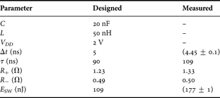
Table 1. Summary of the optimized parameters.
III CIRCUIT DESIGN AND IMPLEMENTATION
The complete chip consists of four building blocks, which are integrated into a monolithic chip and occupy an area of 0.54 mm2. Their circuits and interconnections are depicted in Fig. 7. The dashed lines frame the different parts of the circuit, already known from the system model in Figs. 1 and 2. The starting point for the design of each block is the set of optimized parameters of the buck converter model, which is derived in the last section and summarized in Table 1.

Fig. 7. Complete circuit of the designed buck converter.
A) Envelope detector
The circuit of this block is well known as diode detector. The block capacitor C 0 decouples the DC part of the RF input signal. Only the positive half-wave of the remaining signal passes the Schottky diode D1. An RC filter, which consists of R 1, R 2, C 1, and C 2 suppresses the carrier of the W-CDMA modulated RF signal and implements the derivation in (17). Its transfer function has a pole of order two at f 1 = 15 MHZ which is about four times higher than the chip rate of the W-CDMA signal and a simple zero at
 $$f_2=\displaystyle{{\alpha _{0.5} } \over {2\pi \beta _{0.5} }}=\displaystyle{{\alpha _{0.5} } \over {2\pi R_2 C_2 }}=2.31\, {\rm MHz}.\eqno\lpar42\rpar$$
Thus, a good carrier rejection is achieved, and simultaneously the distortion of the envelope signal is acceptable. The comparator uses current signals. Hence, a current mirror transfers the current through R 1 (output signal of the RC filter) to the envelope detector output current I −. To avoid an input power dependent offset of this signal, a dummy diode detector is employed. The minimal output voltage of the buck converter V 0 is adjusted by the external resistor R 3.
B) Comparator
The output current of the proportional differential feedback I + is inverted by a current mirror and fed to the input of a CMOS inverter (T1 and T2). Thus, the input current of the inverter is the difference ΔI between the I + and I −, the output currents of the proportional differential feedback and the envelope detector. This small part of the whole block already shows the desired behavior: if ΔI is negative the inverter output switches to the supply voltage or else to ground. To increase the speed of the comparator a chain of multiple stages with low gain is preferred over one stage with a high gain [Reference Chen, Shi and Lu11]. Hence, the gain of the inverter is reduced by degeneration. For this purpose, T3 is operated in linear region to form a feedback resistor. Two adjacent common-source stages compensate the gain losses due to the degeneration. With the help of this technique a very low delay time of 1.9 ns is achieved. The output of the last source stage drives a chain of seven CMOS inverters. Three of them belong to the comparator. They ensure that the input signal of the power switches, formed by the remaining four inverters, is rail to rail.
C) Power switches
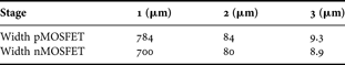
As already mentioned the power switches are formed by a chain of four tapered CMOS Inverters. They have a separate voltage supply to avoid interferences with the other blocks of the circuit. About 65% of the chip area (without pads) is occupied by them. Figure 6 shows the configuration of the power switches, which are an optimum trade-off between efficiency and speed. In this configuration the pMOSFET of the biggest inverter in the tapered chain has a width of w + = 7100 µm and the corresponding nMOSFET has a width of w − = 5900 µm. The dimensions of the driver stages in the chain result from the tapering factor v = 9 and are listed in Table 2.
Table 2. Dimension of the driver stages of the power switches.
In conjunction with the comparator transient simulations show a total delay Δt of 4 ns. To compensate process variations, this value is consciously a little bit smaller than the one calculated in Section II(C).
D) Proportional differential feedback
To make the design more flexible, the feedback circuit processes an input signal range between zero and 1 V. In doing so the ratio between the envelope of the RF input signal and the output voltage V is adjustable by an external voltage divider (R 4 and R 5). Although the PA parameter V H can be fine tuned during the measurements. As the comparator requires a current signal, the input voltage is converted to the output current I + by a source follower. The capacitor C 3 in its load impedance induces the desired differentiating behavior
 $$\tau = R_6 C_3 = 90\, {\rm ns}.\eqno\lpar43\rpar$$
A level shifter, which consists of T4 and T5, guarantees that the transistor of the adjacent source follower does not leave the saturation region over the complete input voltage range.
IV MEASUREMENTS
Because of the external capacitor and inductor, which form the output filter, measurements were performed on a PCB, which houses the chip (shown by Fig. 8a) and all external components. The major challenge of the PCB design is the total parasitic inductance L P in the power switches voltage supply. Because they switch high currents up to 400 mA in very short periods of time (about 500 ps), even a small inductance causes large voltage spikes. Thereby in worst case the supply voltage of the power switches raises transiently beyond the breakdown voltage of the used CMOS transistors. To avoid such conditions there are three possibilities: The supply voltage, the parasitic inductance, or both of them have to be reduced. The diagram in Fig. 9 shows the maximum supply voltage V DD (plotted over L P), which guarantees that the breakdown voltage of 3.6 V is not exceeded. These results were obtained by a parametric transient simulation.

Fig. 8. Realization of the power switches voltage supply. (a) Photo of the fabricated chip (b) Model of the connection between the chip and the decoupling capacitor CB (only the upper half is shown)

Fig. 9. The maximum supply voltage V DD of the power switches as a function of the parasitic inductance L P and the current I = {0, 200 mA, 400 mA}.
An external capacitor C B with a value of 100 nF and an extreme low equivalent series inductance (ESL) of 200 pH decouple the fast changing currents form the rest of the PCB. So only the tracks and wires, which connect it to the chip, have to be taken into account. To keep them as small as possible, the capacitor is placed direct under the chip on the bottom side of the board. On account of the layout's symmetry, it is adequate to analyze only the upper half of these connections. They are depicted by Fig. 8a. The decoupling capacitor has eight terminals, four on each side. They connect alternating the two plates of the capacitor. Hence, the fast changing currents ΔI DD in two adjoining tracks/bond wires are always in opposite directions. So the magnetic fields created by them, partly compensate each other. Thus, the parasitic inductances can be decreased significantly. The electromagnetic analysis software Sonnet® calculates a L P of 943 pH for the described geometry. Hence, according to Fig. 9 the maximum supply voltage of the power switches (with a load of 400 mA) is 2.3 V. That is why the low-power mode of the PA (RMPA2265) is used. The high-power mode would need a supply voltage of 3.3 V.
A) Model parameters of the buck converter
In order to quantify the resistances R + and R − of the power switches, the input V Sens of the chip is connected to an external voltage source. By increasing or rather decreasing its voltage, the state of the power switches can be toggle. A constant current source is applied to the output of the buck converter. For both states of the switches its current is swept from −200 to 200 mA. Through the measurement of the output voltage V two voltage–current characteristics arise. Each of them is approximated well by a linear function, whose slope is equal to the resistance in demand.
To find out the value of the time constant τ, the input V Sens is connected to a sine wave generator. The amplitude and offset of this generator are chosen in a way, that the power switches can be fixed in both states (without any further switching cycles) by varying the bias current I B. For different frequencies f of the sine wave I B is adjusted, until the power switches stop changing their state and only the one, which connects the output of the chip to ground, is active. After a sweep over a frequency range from 100 to 10 MHz the amplitude of the generator is set to zero (its offset is maintained). The bias current is adjusted like before and its value is assigned to the variable I B0. The approximation of the measurements by the function
 $$I_B \lpar \,f\rpar = I_{B0} - K \lpar 1 + \tau 2\pi f\rpar \comma \; \eqno\lpar44\rpar$$
results in the demanded time constant.
In an additional measurement, the buck converter is operated without a load (I L = 0 and R L → ∞). Its output voltage V is set by means of an RF signal generator, which feeds an unmodulated 1.95 GHz carrier with the power PI in the input of the envelope detector. The output of the power switches is connected to an oscilloscope. It is used to measure the period of time Δt 0 during which the switch to the supply voltage is active and Δt 1 vice versa. Furthermore, the average current IDD drained from the source V DD is recorded. Because the input voltage V E of the DC–DC converter remains constant during each measurement, its state x 0 has to fulfill the following equation:
 $$x_0 = {\cal T}_{\Delta t_1}^+ {\cal T}_{\Delta t_0}^{-} x_0. \eqno\lpar45\rpar$$
So x 0 and the corresponding state x 1 after the time Δt 0 can be calculated as follows:
 $$x_0 = \left(E - {\rm e}^{A_+ \Delta t_1} e^{A_ - \Delta t_0} \right)^{ - 1} {\cal T}_{\Delta t_1}^+ {\cal T}_{\Delta t_0}^{-} 0\comma \; \eqno\lpar46\rpar$$
 $$x_1 = {\cal T}_{\Delta t_0}^{-} x_0. \eqno\lpar47\rpar$$
Due to V E = const. the equation
 $$c^T \left({\cal T}_{ - \Delta t}^{+} x_0 - {\cal T}_{ - \Delta t}^ - x_1 \right)= 0 \eqno\lpar48\rpar$$
is valid. It is used to obtain the value of Δt, because all other variables it contains are already known.
The dynamic losses of the power switches can also be derived from the measured data
 $$P_{SW} \lpar f_0\rpar = E_{SW} f_0 = V_{DD} \bar{I}_{DD} - \left({\cal L}_{\Delta t_0}^{-} x_0 + {\cal L}_{\Delta t_1}^{+} x_1 \right)f_0. \eqno\lpar49\rpar$$
With the help of this relation, E SW can be calculated easily. To get more accurate results, the shown procedure is repeated for different output voltages V. Table 1 summarizes the measured parameters of the buck converter. The parameters specified during the design of the circuit and the measured ones match well.
B) Complete system
Now the designed circuit is used to modulate the supply voltage of a commercial standard W-CDMA PA (RMPA2265). Because this PA is a two-stage design, only its second and final stage is connected to the buck converter. Its first stage is supplied by a constant supply voltage and is neglected in the following considerations. The RMPA2265 is operated in the low-power mode, which has a linear output power of 16 dBm. Two properties have to be determined for the PA with a fixed supply voltage and the EF configuration: the efficiency and the linearity. The efficiency is defined as the ratio of the complete system power consumption and the output power of the PA. To compare both configurations the efficiency gain
 $$G = {\eta_{EF} \over \eta} \eqno\lpar50\rpar$$
is introduced. In this equation, ηEF enotes the efficiency of the EF configuration and η describes the efficiency of the PA with a fixed supply voltage. As a measure for the linearity of the PA the adjacent channel leakage power ratio (ACLR) of its output signal is used. It is measured by a R&S® FSU 67 spectrum analyzer in the first and second, left and right adjacent channel. The W-CDMA modulated test signalFootnote 2, which feeds the PA, is generated by a R&S® SMBV100A vector signal generator. Figure 10 depicts the results of the measurements. It shows a significant efficiency gain at low output powers PO. The values of G can also be calculated with the mathematical model of the buck converter

Fig. 10. Comparison between the fixed supply voltage and the EF (with the proposed buck converter and an ideal supply voltage modulator) configuration of the RMPA 2265.
 $$G = {\vint \left({V_E \lpar \xi h\rpar \over R_L} - I_L \right)V_E \lpar \xi h\rpar p_F \lpar h\comma \; \dot{h}\comma \; \ddot{h}\rpar \, dh \, d \dot{h} \, d \ddot{h} \over \vint \left(P_U \lpar \xi h\comma \; \xi \dot{h}\comma \; \xi \ddot{h}\rpar + P_L \lpar \xi h\comma \; \xi \dot{h}\comma \; \xi \ddot{h}\rpar \right)p_F \lpar h\comma \; \dot{h}\comma \; \ddot{h}\rpar \, dh \, d\dot{h} \, d \ddot{h}}\comma \;$$
 $${\rm with}\; \xi = \sqrt{{\bar{P}_O \over \bar{P}_{Om}}}\comma \; \quad{\bar{P}_{Om}} = 16\, \hbox{dBm}. \eqno\lpar51\rpar$$
The forecast of the model matches the measurements very well. This is quite impressive, considering that a simplified and linearized model was used for analysis. The ACLR leaves slightly the range admitted by the W-CDMA standard. This effect can have two different causes: either the DC–DC converter is not capable to follow the envelope of the RF input signal all the time. Or the gain and phase shift of the PA changes with its supply voltage. Such behavior, which was shown for the RMPA2265, makes it not very suitable for an EF PA at all. To emphasize this assumption the ACLR estimation method, presented in [Reference Sundstrom12], is applied on a RMPA2265 whose supply voltage is modulated ideally. The results are also depicted in Fig. 10. They show that even an ideal modulation of the supply voltage would cause a significant rise of the ACLR. Due to the dependency of the PA gain and phase on its supply voltage, the output ripple of the buck converter is mixed with the RF signal. This effect causes the high values of the ACLR (especially at low output powers) in the second adjacent channels. The following properties of the design were observed with an oscilloscope and are completely satisfying.
The average efficiency gain
 $$\bar{G} = \vint p_S \left(\bar{P}_O {P_{27dBm} \over P_{16dBm}} \right)G \lpar \bar{P}_O\rpar \, d\bar{P}_O = 2.03\eqno\lpar52\rpar$$
is obtained by weighting the measured values with their probability. Furthermore, the average efficiency gain with an ideal supply voltage modulator is defined as follows:
 $$\bar{G}_I = \vint {V_{DD} \over V_E \lpar \xi h\rpar } p_M \lpar h\comma \; \dot{h}\comma \; \ddot{h}\rpar \, dh \, d\dot{h} \, d\ddot{h} = 3.19. \eqno\lpar53\rpar$$
The ratio between these two quantities is approximately the efficiency of the buck converter
 $${\bar{G} \over \bar{G}_I} \approx \eta_B = 63.8\percnt . \eqno\lpar54\rpar$$
The value of ηB as also derived from the results of the measurements and is very similar to the one which was determined during the parameter optimization (shown in Fig. 6 with a cross).
V CONCLUSION
The buck converter presented in this work, fulfills all requirements of an envelope amplifier for a modern efficiency enhancement system. It shows both a high average efficiency of 63.5% and the dynamic properties to follow the fast changing envelope signal of a W-CMDA modulated RF signal. Because the design only uses CMOS devices, it is perfectly suited for economic large-scale productions. By means of the proposed design flow the circuit can be adapted to a wide range of different communication standards and IC technologies. The base of this flow is the mathematical model of the DC–DC converter and the envelope signal. Its accuracy is confirmed by measurements. In an EF configuration the buck converter doubles the average efficiency of an industry standard W-CDMA PA (RMPA2265). The DC current of this PA varies over the wide range from 30 to 160 mA proportional to the square root of its output power. Hence, the RMPA2265 has already – without any efficiency enhancement techniques – a much better back-off efficiency as comparable PAs in class A configuration. That is why the presented design has to cope with a challenge, which cannot be found for a setup with a class A PA. A high average efficiency of the DC–DC converter despite a wide range of its output current.
Due to restrictions of the used technology only small supply voltages could be used. The employment of technologies which are better suited for switching regulators could increase the supply voltage and also the efficiency gain significantly.
ACKNOWLEDGEMENTS
This work was partly funded by the Federal Ministry of Education and Research (BMBF) in the excellence cluster Cool Silicon, project Cool Broadcast Repeater.
 Falk Haßler was born in Eberswalde-Finow, Germany in 1983. He received the Diploma degree in electrical engineering from Dresden University of Technology, Dresden, Germany, in 2010.
 Frank Ellinger (S'97-M'01-SM'06) graduated from the University of Ulm, Germany, in electrical engineering (EE) in 1996. He received an MBA and a Ph.D. degree in EE from ETH Zürich (ETHZ), Switzerland, in 2001, and the habilitation degree in high frequency circuit design from ETHZ in 2004. Since August 2006 he is full professor and head of the Chair for Circuit Design and Network Theory at the Dresden University of Technology, Germany. He is a member of the management board of the Cool Silicon e.V. having 65 partners from industry and academia. From 2001–2006, he has been head of the RFIC design group of the Electronics Laboratory at the ETHZ, and a project leader of the IBM/ETHZ Competence Center for Advanced Silicon Electronics hosted at IBM Research in Rüschlikon. Prof. Ellinger was coordinator of the EU funded projects RESOLUTION and MIMAX. He published more than 170 refereed scientific papers.
 Udo Jörges was born in Steinach (Thuringia), Germay, in 1952. He received the Diploma degree in electrical engineering, Ph.D. degree, and Habilitation degree in electrical engineering from the Dresden University of Technology, Dresden, Germay, in 1975, 1979, and 1985, respectively. Since 1999, he has been an Associate Professor, and since 2006, the Chair for circuit design and network theory with the Dresden University of Technology. His main research interests are in the field of circuit theory and the design of analog ICs.
 Robert Wolf was born in Karl-Marx-Stadt (nowadays call Chemnitz), Germany, in 1984. He received the Masters degree in electrical engineering from the Dresden University of Technology (TUD), Dresden, Germany, in 2009, and is currently working toward the Ph.D. degree at TUD.
 Bastian Lindner was born in Wuppertal, Germany, in 1981. He received the Masters degree in electrical engineering from the Dresden University of Technology (TUD), Dresden, Germany, in 2011.


