I. INTRODUCTION
Nowadays, the development of communication systems has led engineers to require low-profile, light weight and monolithic antennas, especially in many wireless communication systems such as satellite, aircraft, and some radar systems.
Recently, slot antennas based on substrate-integrated waveguide (SIW) technology have been attracted increasing attention due to many advantages of both waveguide and printed circuit board, such as low-profile, low-cost, high-quality factor and high-power-handling capability with self-consistent electrical shielding and easy integration with planar microwave circuits [Reference Hirokawa and Ando1–Reference Hong4].
There are several papers subjected to cavity-backed slot antennas [Reference Hikage, Omiya and Itoh5–Reference Luo, Hu, Dong and Sun9]. However, most of the previous researches have been relied on designing cavity-backed slot antennas by conventional metallic cavities [Reference Hikage, Omiya and Itoh5–Reference Lee, Harackiewicz, Jung and Park7]. This feature is undesirable as it makes the antenna a three-dimensional (3D) structure.
A wideband double-layer slot array antenna in the 12-GHz band was proposed in [Reference Jung, Lee, Kang, Han and Lee10, Reference Lee, Jung and Yang11], in which a parallel feeding waveguide is used to excite the several 2 × 4-element cavity-backed subarrays. In the millimeter wave band, multilayer structure cannot be fabricated easily by conventional techniques such as machining or die-casting. Therefore in [Reference Miura, Hirokawa, Ando, Shibuya and Yoshida12] another similar double-layer cavity-backed slot array antenna in 60 GHz band was proposed, in which the diffusion bonding of laminated thin metal etching plates is adopted for the fabrication of a double-layer full-corporate-feed waveguide slot array antenna. In contrast with multiple layer structure antennas in [Reference Jung, Lee, Kang, Han and Lee10, Reference Lee, Jung and Yang11, Reference Miura, Hirokawa, Ando, Shibuya and Yoshida12], the SIW structures can be used widely from microwave band up to millimeter wave band without loss of significant accuracy.
A low-profile, linearly polarized, cavity-backed slot antenna based on SIW has been firstly proposed in [Reference Luo, Hu, Dong and Sun9], in which a grounded coplanar waveguide (GCPW), subminiature version A (SMA), printed circuit board (PCB) feeding network is used to excite the TE120 mode of a cavity. In [Reference Bohórquez, Forero Pedraza, Herrera Pinzón, Castiblanco, Peña and Guarnizo13], another similar SIW cavity-backed slot antenna is proposed in which a rectangular slot radiator has been replaced by a meandered slot line to exploit the properties of the cavity TE101 mode to achieve the smallest possible cavity and lower power loss. However, the overall antenna performances such as resonant frequency, impedance bandwidth, radiation properties, etc. are greatly relied on meandered line's parameters leading to a complex design procedure, which is based on exact optimization. Also in [Reference Luo, Hu, Liang, Yu and Sun14] another low-profile SIW cavity-backed, crossed slot antenna is presented, which is operated in dual frequencies and produced dual linear and circular polarizations.
It seems that in all above references the radiating slot's and/or feeding's parameters have been well selected to achieve a proper mode excitation without any changing in cavity structure. Thus, for this type of SIW cavities the modal solution that was provided for traditional metallic cavities can be adopted and used without significant loss of accuracy as was done in [Reference Woo, Han, Yun, Nam and Oh15].
Also, in [Reference Luo, Zhang, Dong, Li and Sun16] another cavity-backed slot antenna was proposed, in which a diagonal GCPW line is used to excite high-order cavity resonance in the large SIW cavity to generate radiations. However, the planar transmission lines such as microstrip lines or CPW lines are not suitable for using in the millimeter wave band because they possess higher ohmic losses in high frequencies. This limitation can be more bolded when this type of antenna is used as an antenna element in array configuration where a GCPW-feeding network is used to excite the array especially in high frequencies (mm wave band).
In this paper, a new type of cavity-backed slot antennas based on modified SIW cavity is proposed. This modification was done by introducing metallic via-holes in a main cavity. In addition, to acquire insight of antenna's performance, the modified cavity's field distribution is studied. To do so, the mode-matching technique is exploited to represent the equations for the field distribution of the TE and TM modes in the modified cavity. The validity of this analysis is verified by comparing our results with simulated results that is obtained by Ansoft's HFSS as well as experimental results. Two types of the proposed SIW cavity-backed slot antenna forming two different polarizations (horizontal and vertical) are analyzed, simulated, and fabricated. A theoretical model combined with a numerical analysis of the antenna, using Ansoft's HFSS, along with the parametric analysis of the effects of each parameter on the antenna's performance, is introduced. The simulated and measured results are presented and discussed.
II. FIELD DESCRIPTION IN MODIFIED CAVITY
Figure 1 illustrates a schematic view of the proposed modified SIW cavity resonator. The proposed cavity is placed on the RO4003™ (Rogers) substrate, with a relative permittivity of 3.55, a loss tangent of 0.0027, and a thickness of 32 mil. As is evident from Fig. 1, the cavity is divided onto four subsections by embedding the metallic posts in the middle of each edge of main cavity. As a consequence, the field distribution as well as excitation mode of cavity are altered from that in a parent cavity due to perturbations made by the dividing vias/walls. Therefore, in this section the field distribution of modified cavity using mode-matching technique is introduced.

Fig. 1. Top view of the proposed modified SIW cavity. The optimum physically dimensions are: L cv = 28.18 mm; W cv = 22.5 mm; h = 6.94 mm; h 1 = 6.4 mm; p v = 1.3 mm; and d = 1 mm.
In SIW structures, the leakage losses are determined by the vias diameter d and spacing p v. Thus, these parameters can be well chosen to minimize the leakage losses. In this manner, the rows of metallic posts behave as solid metallic walls. Thus, in this paper to reduce the complexity, the metallic rows are replaced by equivalent metallic walls without significant loss of accuracy [Reference Woo, Han, Yun, Nam and Oh15]. However, the dimensions of the cavity are changed after using metallic walls according to Yan et al. [Reference Yan, Hong, Hua, Chen, Wu and Cui17]. Despite that the equivalence was previously developed in [Reference Yan, Hong, Hua, Chen, Wu and Cui17] is for propagating waveguide structures, it can be used for cavities but by performing some tuning in equivalent dimensions. However, here we extend this equivalence to cavities as well, upon taking the resonance nature of the structure in hand into account. To do so, the cavity was modeled in a transmission setup by HFSS, in which the coaxial probes are used to excite the cavity at the input and output sides of it (with minimal cavity perturbation due to coaxial probes penetration), as shown in Fig. 2.
Fig. 2. (a) SIW cavity and equivalent cavity with solid walls and relevant parameters. (b) A schematic view of cavity in a transmission setup with coaxial input and output excitations.
To estimate the leakage loss at resonance an extensive parametric study varying both the diameter and spacing have been run in steps and the S-parameters have been calculated. The leakage loss is given by:
 $$L_{Leakage}=- 10\, \log \left({\lpar S_{11} \rpar ^2+\lpar S_{22} \rpar ^2 } \right).$$
Note that in our model perfect electric conductors and zero loss dielectric substrate have been assumed to isolate the leakage loss from the conductor and dielectric losses.
Meanwhile, an equivalence parameter “R eq” have been defined as:
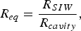 $$R_{eq}=\displaystyle{{R_{SIW} } \over {R_{cavity} }}\comma \;$$
where R SIW and R cavity are the radii of the SIW and the equivalent solid wall cavities resonating at the same frequency. Figure 3(a) demonstrates the calculated equivalence parameter “R eq” versus the via holes' spacing and diameter normalized to the resonant wavelength of the cavity that are presented by the contour plot. As is expected R eq ranges from 0.98 to 1.02 when the vias are changed from sparsely spaced relatively small via-holes to densely spaced relatively large via holes. Meanwhile, Fig. 3(b) shows a contour plot for the leakage loss in dB. It should be noted that it is essential to select via holes' diameter and spacing that minimize the leakage loss. Subsequently, the equivalent cavity with solid walls is defined according to Fig. 3(a).
Fig. 3. Characteristics of the rectangular SIW cavity in contour plots against the via-holes diameter (D/λ g) and spacing (S/λ g) normalized to the resonance wavelength of the cavity, assuming ε r = 3.55 and h = 32 mil. (a) Equivalence parameter to the solid wall cavity “R eq”. (b) Leakage loss in dB.
Based on the aforementioned analysis, the SIW cavities to be used in the cavity-backed antennas have been implemented with via-holes of 0.051 λg in diameter with a linear spacing of 0.066 λg.
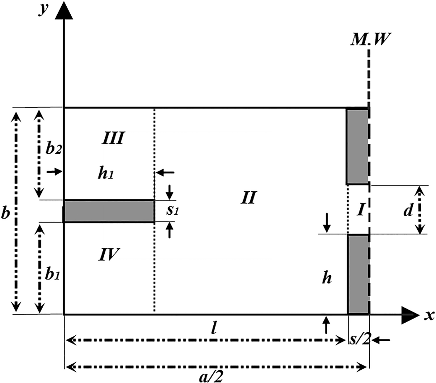
The model to be analyzed, a half section of a modified cavity, is shown in Fig. 4. An approximate solution at the resonant frequency will be found by assuming a single term in the gap region (region I) and N expansion terms in through regions (regions II, III, and IV) and with the application of the boundary conditions on the tangential fields at x = h 1 and l. The field distribution of the TE and TM modes in a modified cavity of Fig. 2 is written in Appendix A. Enforcing the boundary conditions on the tangential fields at x = h 1 and l, after some mathematical manipulation, leads to the following equations:
Fig. 4. Equivalent modified cavity with magnetic wall's symmetry.
For TE modes:
 $$\eqalign{&{A_m}{e^{ - j{\alpha _m}l}} - {B_m}{e^{j{\alpha _m}l}} = \displaystyle{{ - 2b(k_c^2 - \alpha _m^2 )} \over {{{(m\pi )}^2}j{\alpha _m}}}\cos \left( {{k_c}\displaystyle{s \over 2}} \right) \cr & \quad\times \left( {\sin \left( {\displaystyle{{m\pi (h + d)} \over b}} \right) - \sin \left( {\displaystyle{{m\pi h} \over b}} \right)} \right)\comma \;}$$
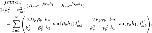 $$\eqalign{& \displaystyle{{jm\pi {\alpha _m}} \over {2(k_c^2 - \alpha _m^2 )}}({A_m}{e^{ - j{\alpha _m}{h_1}}} - {B_m}{e^{j{\alpha _m}{h_1}}}) \cr & \quad= \sum\limits_{k = 1}^N {\left( {\displaystyle{{2{D_k}{\beta _k}} \over {k_c^2 - \beta _k^2 }}\displaystyle{{k\pi } \over {{b_2}}}\sin ({\beta _k}{h_1})I_{mk}^i + \displaystyle{{2{F_k}{\gamma _k}} \over {k_c^2 - \gamma _k^2 }}\displaystyle{{k\pi } \over {{b_1}}}\sin ({\gamma _k}{h_1})I_{mk}^{ii} } \right)},}$$
 $$\eqalign{& {D_k}\displaystyle{{k_c^2 (k\pi )} \over {k_c^2 - \beta _k^2 }}\cos ({\beta _k}{h_1}) \cr & \quad = \sum\limits_{n = 1}^N {\displaystyle{{k_c^2 } \over {k_c^2 - \alpha _n^2 }}} \displaystyle{{n\pi } \over b}\left[ {{A_n}{e^{ - j{\alpha _n}{h_1}}} + {B_n}{e^{j{\alpha _n}{h_1}}}} \right]I_{nk}^i ,}$$
 $$\eqalign{& {F_k}\displaystyle{{k_c^2 (k\pi )} \over {k_c^2 - \gamma _k^2 }}\cos ({\gamma _k}{h_1}) \cr & \quad = \sum\limits_{n = 1}^N {\displaystyle{{k_c^2 } \over {k_c^2 - \alpha _n^2 }}} \displaystyle{{n\pi } \over b}\left[ {{A_n}{e^{ - j{\alpha _n}{h_1}}} + {B_n}{e^{j{\alpha _n}{h_1}}}} \right]I_{nk}^{ii}.}$$
For TM modes:
 $$\eqalign{& {A_m}{e^{ - j{\alpha _m}l}} + {B_m}{e^{j{\alpha _m}l}} = j\omega \varepsilon \displaystyle{{k_c^2 - \alpha _m^2 } \over {k_c^2 }}\displaystyle{2 \over {m\pi }}\cos \left( {{k_x}\displaystyle{s \over 2}} \right) \cr & \quad \times\displaystyle{{(\pi /d)} \over {{{(\pi /d)}^2} - {{(m\pi /b)}^2}}}\left( {\sin \left( {\displaystyle{{m\pi (h + d)} \over b}} \right) + \sin \left( {\displaystyle{{m\pi h} \over b}} \right)} \right),}$$
 $$\eqalign{& \displaystyle{{m\pi } \over {2(k_c^2 - \alpha _m^2 )}}({A_m}{e^{ - j{\alpha _m}{h_1}}} + {B_m}{e^{j{\alpha _m}{h_1}}}) \cr & \quad= \sum\limits_{k = 1}^N {\left( {\displaystyle{{j2{D_k}} \over {k_c^2 - \beta _k^2 }}\displaystyle{{k\pi } \over {{b_2}}}\sin ({\beta _k}{h_1})I_{mk}^i + \displaystyle{{j2{F_k}} \over {k_c^2 - \gamma _k^2 }}\displaystyle{{k\pi } \over {{b_1}}}\sin ({\gamma _k}{h_1})I_{mk}^{ii} } \right)},}$$
 $$\eqalign{& {D_k}\displaystyle{{j{\beta _k}(k\pi )} \over {k_c^2 - \beta _k^2 }}\cos ({\beta _k}{h_1}) \cr & \quad = \sum\limits_{n = 1}^N {\displaystyle{{ - j{\alpha _n}} \over {k_c^2 - \alpha _n^2 }}} \displaystyle{{n\pi } \over b}\left[ {{A_n}{e^{ - j{\alpha _n}{h_1}}} - {B_n}{e^{j{\alpha _n}{h_1}}}} \right]I_{nk}^i ,}$$
 $$\eqalign{& {F_k}\displaystyle{{j{\gamma _k}(k\pi )} \over {k_c^2 - \gamma _k^2 }}\cos ({\gamma _k}{h_1}) \cr & \quad = \sum\limits_{n = 1}^N {\displaystyle{{ - j{\alpha _n}} \over {k_c^2 - \alpha _n^2 }}} \displaystyle{{n\pi } \over b}\left[ {{A_n}{e^{ - j{\alpha _n}{h_1}}} - {B_n}{e^{j{\alpha _n}{h_1}}}} \right]I_{nk}^{ii},}$$
where
 $$I_{mn}^i=\vint_0^{b_2 } {\sin \left({\displaystyle{{m\pi y} \over b}} \right)\sin \left({\displaystyle{{n\pi y^\ast } \over {b_2 }}} \right)} \, dy^\ast \comma \;$$
 $$I_{mn}^{ii}=\vint_0^{b_1 } {\sin \left({\displaystyle{{m\pi y} \over b}} \right)\sin \left({\displaystyle{{n\pi y} \over {b_1 }}} \right)} \, dy$$
with m = 1,2, …, N.
Substituting Dk and Fk from (5)/(9) and (6)/(10) into (4)/(8) and with the aid of (3)/(7) gives an N set of linear equations for the An and Bn that can be written in the matrix form as:
 $$\left[{Q_{mn}^A } \right]_{N \times N} \left[{A_m } \right]_{N \times 1}=\left[{Q_{mn}^B } \right]_{N \times N} \left[{B_m } \right]_{N \times 1}\comma \;$$
 $$\left[{B_m } \right]_{N \times 1}=\xi \times e^{ - 2j\alpha _n l} \left[{A_m } \right]_{N \times 1}+\left[{P_m } \right]_{N \times 1}\comma \;$$
where
 $$\xi=\left\{{\matrix{ {1\, \, {\rm for}\, \, {\rm TE}\, \, {\rm modes}} \cr { - 1\, \, {\rm for}\, \, {\rm TM}\, \, {\rm modes}} \cr } } \right\}.$$
Equations (11)–(12) lend themselves well to computer implementation. In numerical solution, only the first few TM/TE modes will be used. Using larger number of modes the accuracy of the fields is improved. Figure 5 shows the percentage error for the TM220 mode fields on the boundaries x = l and h, as a function of the number of modes.
Fig. 5. Field's error versus number of modes.
Also, the field distributions of the proposed modified cavity resonator at three frequencies are shown in Fig. 6. In addition, the results obtained with HFSS are presented for comparison and are in good agreement. Using mode-matching technique to calculate the fields in modified cavity is not only faster than that when simulated by such commercials software, e.g. HFSS, but also provided an insight about antenna's fields behavior that enable optimization of the antenna's performance.
Fig. 6. Field's distributions at three frequencies. (a) Presented method and (b) HFSS results
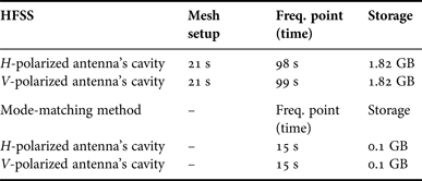
Table 1 illustrates a comparison between CPU time and storage used to simulate the two proposed antennas using finite-element-based commercially available software, HFSS, and modal solution. As is evident from the results, a considerable time and storage saving is achieved using the mode-matching technique introduced in this paper.
Table 1. CPU time and storage (Intel Core-i7 at 3.7 GHz 16 GB RAM).
It should, however, be mentioned that due to use of metallic walls in place of metallic rows of vias and assuming one mode in the gap region, this procedure may be inaccurate for the fields very close to the edge of dividing vias/walls, but it gives reasonable results elsewhere.
III. ANTENNA DESIGN AND STRUCTURE
Figure 7 illustrates the proposed cavity-backed slot antenna. The aforementioned modified cavity is used to feed an array of 2 × 2 slot antenna. The slots are etched on the top wall of each sub-section of the cavity. The cavity is excited in TM220 mode. This mode as is shown in Fig. 6 has a maximum E-filed in each subsection. This feature makes it suitable to etch a slot radiator at each subsection. A feeding short-circuited waveguide on the rear side of the cavity excites the cavity by a coupling longitudinal slot. Also, the SIW waveguide width a SIW is chosen for single fundamental mode operation.
Fig. 7. A schematic view of the horizontally polarized cavity-backed slot antenna: (a) upper substrate including cavity and radiating slots; (b) lower substrate including feeding waveguide and coupling aperture. The optimum physically dimensions are: W sub = 10.85 mm; X off = 1.1 mm; L r = 10.024 mm; W r = 0.88 mm; L cs = 9.99 mm; W cs = 0.42 mm; d SC = 9.62 mm; a SIW = 14.41 mm; and X off = 1.34 mm.
The coupling aperture parameters, L cs, W cs, and X off, and the short-circuit position, dsc, should be optimized to efficiently couple the energy from the SIW-feeding waveguide to radiating element. As an initial value, dsc is chosen to be λ g/4 to ensure the maximum standing wave field intensity. However, a little tuning is needed to achieve a better input matching. Figure 8 shows the effect on the reflection coefficient of the proposed H-polarized antenna (Fig. 7) by the coupling slot length defined by the parameter L cs. The results indicate that by increasing the coupling slot length, L cs, from 8.82 to 12 mm, the resonant frequency of the proposed antenna is shifted down from 10.38 to 10.08 GHz, i.e. 2.96%. Also Fig. 9 gives the reflection coefficient of the antenna with various coupling slot relative position, X off. The results show that an optimum input impedance matching is achievable when the X off is increased to a certain value. However, if X off is increased further more than this value, the impedance matching will deteriorate. It should be noted that the behavior of the horizontally and vertically polarized slot antennas versus variation of such parameters are the same. Thus, the above results only for prototype antenna in Fig. 7 have been provided.
Fig. 8. The impact of coupling slot length, L cs, on reflection coefficient of the antenna.
Fig. 9. The impact of coupling slot relative position, X off, on reflection coefficient of the antenna.
To achieve a good directional radiation pattern, the radiating slots should be excited in uniform distribution, i.e. they should have the specification that the slot voltage distribution be equi-phase and equi-magnitude. Based on the feeding scheme which is used in the proposed antenna, as is depicted in Fig. 7, and the filed distribution of the cavity's TM220 mode, all the sub-cavities are excited in almost equi-magnitude but the sub-cavities, which are placed in the opposite side of reference plane of yy′ be excited in the anti-phase, leading to an antenna with a deep null in the broadside direction, like as a difference pattern. To overcome this situation and achieve a uniform distribution, the radiating slot's offsets, which are placed in the opposite side of reference plane of yy′, should be opposite with respect to centerline of each sub-cavity. This is the reason which is led the radiating slot's position to be changed in two types of proposed antennas as are shown in Figs 12(a) and 12(b).
IV. ANTENNA MECHANISM DESCRIPTION
The proposed cavity-backed slot antenna consists of four similar radiating sub-sections; each of them includes a radiating slot etched on a sub-cavity in which the energy is coupled through the inductive window from the feeding SIW to the radiating element. The inductive window can be modeled as a shunt inductance. Using mode matching technique at the boundary x = l, the inductive impedance of one side of modified cavity can be calculated. However, the exact model of inductive window that is shown in Fig. 10, cannot be evaluated by this method. The simulation results show that the inductive window has two fundamental effects on the performance of the antenna, first is controlling the amount of energy coupled from the feeding SIW to the radiating element and second is providing a first-order matching network, which alleviates the sensitivity of the overall antenna matching to the radiating slot's parameters. It can provide a more convenience in design of antenna, especially in array configuration where mutual coupling between antenna radiating elements are degraded antenna performances and added more complexity to design.
Fig. 10. The impact of radiating slot length, L r, on reflection coefficient of the horizontally polarized slot antenna and a schematic view of inductive window in a sub-cavity.
Figure 10 gives the reflection coefficient of the H-polarized antenna (Fig. 7) with various radiating slot length, L r. The results show that by increasing the radiating slot length, L r, from 8.82 to 12 mm, the resonant frequency of the proposed antenna is shifted down from 10.22 to 10.06 GHz, i.e. 1.57%. Comparing to the results provided in Fig. 8, it is evident that the proposed antenna, due to the effect of inductive window, is not very sensitive to change in the radiating slot's length.
V. SIW-TO-MICROSTRIP LINE TRANSITION
The transitions between planar transmission lines and SIW structures, which can be integrated on the same substrate, play a crucial role in design and implementation of the SIW components and antennas. The microstrip line and coplanar waveguide (CPW) are two main candidates to integrate with SIW structures. Thus, in this paper, to couple energy from the SMA edge connector to the cavity-backed SIW slot antenna for measurements, a planar transition from microstrip to SIW, based on a simple second-order taper (Fig. 11), has been designed and optimized using the HFSS software to in-band insertion loss of better than 0.5 dB. The SIW–microstrip-transition (SIW–MT) parameters were optimized to match the microstrip line fundamental mode to the SIW waveguide TE10 fundamental mode. A second-order taper is used to achieve a better reflection coefficient in a wide-operating frequency band. Figure 11 illustrates the simulated reflection coefficient as well as insertion loss of the optimized back-to-back SIW–MT, showing that a wide impedance bandwidth, ranging from 9 to 11 GHz, for S 11 < −25 dB is achievable.
Fig. 11. The simulated S 11 and S 12 of the optimized back to back SIW–MIC transition. The optimum dimensions are: L t1 = 6.55 mm; W t1 = 4.8 mm; L t2 = 6.75 mm; and W t2 = 3.75 mm.
VI. SIMULATED AND EMPIRICAL RESULTS
The aim of this work is to introduce a gain-enhanced method of cavity-backed SIW slot antenna using of a high-order cavity resonance. In addition, these new type of cavity-backed SIW slot antennas can provide a simple and robust design along with a low-profile structure. In addition, the gain-enhanced method proposed in the present paper can be extended for using even higher-order cavity resonances such as the TM440 with eight radiating slots, the TM660 with 12 radiating slots, etc. To validate the theoretical analysis, two types of proposed antenna forming two different polarizations (horizontal and vertical) are analyzed, simulated, and fabricated. The simulated as well as measured results have been provided, indicating a good agreement with simulated results.
Figure 12 gives the simulated as well as empirical reflection coefficients for two-antenna prototypes, showing that a bandwidth of 0.6% (prototype antenna of Fig. 12(a)) and 0.9% (prototype antenna of Fig. 12(b)) is achievable. The results show that the radiation is only generated at the certain frequency within a wide-frequency range, making them suitable for some applications in which highly isolated antenna is required for rejecting out-of-band interference signals [Reference Luo, Hu, Dong and Sun9]. Also, the simulated and measured radiation patterns of two antenna prototypes (horizontally polarized and vertically polarized antennas) at resonant frequency in two orthogonal planes (the x–z and y–z planes), are shown in Figs 13 and 14, respectively. The results show that the cross-polarization level is quite low, i.e. <− 25 dB (antenna prototype in Fig. 12(a)) and is <− 20 dB (antenna prototype in Fig. 12(b)), indicating that the proposed antennas exhibit high polarization purity. However, by comparing the simulated radiation patterns with measured ones, a little bit deformation is observed. The disagreements in cross-polarization patterns are more obvious. Measurement errors (especially in dynamic range limitation) and manufacturing errors (PCB manufacturing tolerances and assembly errors) cause the measured cross-polarization radiation patterns to be different from simulated ones. In spite of that, as mentioned earlier, the results indicate that the proposed antennas exhibit high polarization purity.
Fig. 12. Measured and simulated reflection coefficient of the (a) H-polarized and (b) V-polarized slot antennas. For V-polarized slot antenna L cs = 9.1 mm and X off = 1.45 mm; All other physically dimensions are the same as H-polarized one.
Fig. 13. (a) Measured and (b) simulated radiation patterns of the H-polarized antenna in two orthogonal planes.
Fig. 14. (a) Measured and (b) simulated radiation patterns of the V-polarized antenna in two orthogonal planes.
The main beam of the antenna has a maximum co-polarization gain of 8.4 dBi for horizontally polarized antenna and 7.9 dBi for vertically polarized antenna. Furthermore, the proposed antennas exhibit the advantages of simple feed network and more compact size in comparison with an antenna array, which has the same gain. The simulated results show that the proposed antennas have almost more than 35 dB front-to-back (F/B) level, which is 22 and 19 dB higher than that of the antennas introduced in [Reference Luo, Hu, Dong and Sun9, Reference Bohórquez, Forero Pedraza, Herrera Pinzón, Castiblanco, Peña and Guarnizo13], respectively. However, the measured results show that the proposed antennas have almost 15 dB F/B, indicating that the proposed antennas exhibit a low back lobe.
VII. CONCLUSION
By placing the metallic via-holes in a main cavity of a slot antenna, a new type of gain-enhanced SIW cavity-backed slot antennas is introduced. Moreover, to acquire the insight of modified cavity's field distribution, a comprehensive modal study was performed on the modified cavity to fully understand the effects of the dividing walls on the cavity's field distribution. Also, compared with HFSS, the modal solution that is proposed in the present paper provide a considerable time and storage saving. In addition, the gain-enhanced method proposed in this paper can be extended for using even higher-order cavity resonances such as TM440 and TM660, etc. if higher gain is desirable. Two types of the proposed SIW cavity-backed slot antenna forming two different polarizations (horizontal and vertical) are analyzed, simulated, and fabricated. The measured results show that antenna has a good directional radiation pattern with almost gain of 8.2 dBi, and high F/B of almost >15 dB (for measured data) and almost >35 dB (for simulated patterns) and a very low cross-polarization of almost <− 20 dB. The antennas proposed in this paper have many advantages in terms of: simple design, low-power loss, low-profile, high polarization purity, high F/B, and ease of use as an antenna element, in array configuration. Furthermore, the proposed antennas exhibit the advantages of simple feed network and more compact size in comparison with an antenna array, which has the same gain. These interesting features make the proposed antennas suitable to use in many wireless applications.
Appendix A
The field distribution of the TE and TM modes in a modified cavity of Fig. 2 can be written as:
TE modes:
 $$\bar E_I^y=\cos \left({k_c \left({\displaystyle{a \over 2} - x} \right)} \right)\sin \left({\displaystyle{{p\pi } \over c}z} \right)\bar a_y\comma \;$$
 $$\eqalign{& {\bar H}_I = \left[{ - \displaystyle{{{k_z}} \over {\omega \mu }}\cos \left({{k_c}\left( {\displaystyle{a \over 2} - x} \right)} \right)\cos \left( {\displaystyle{{p\pi } \over c}z} \right){{\bar a}_x}}\right. \cr & \qquad \quad \left. { - \displaystyle{{{k_c}} \over {j\omega \mu }}\sin \left( {{k_c}\left( {\displaystyle{a \over 2} - x} \right)} \right)\sin \left( {\displaystyle{{p\pi } \over c}z} \right)\bar a} \right],}$$
 $$\eqalign{ {{\bar E}_{II}} &= \left[ {\sum\limits_{n = 1}^N {\left( {({A_n}{e^{ - j{\alpha _n}x}} + {B_n}{e^{j{\alpha _n}x}})\sin \left( {\displaystyle{{n\pi } \over b}y} \right)} \right)} \sin \left( {\displaystyle{{p\pi } \over c}z} \right){{\bar a}_x}} \right. \cr & \quad +\left\{ {{A_0}\sin ({k_c}x) + \sum\limits_{n = 1}^N {\left( {\displaystyle{{ - j{\alpha _n}} \over {k_c^2 - \alpha _n^2 }}\left( {\displaystyle{{n\pi } \over b}} \right)({A_n}{e^{ - j{\alpha _n}x}} - {B_n}{e^{j{\alpha _n}x}})} \right.} } \right. \cr & \quad\times \left. {\cos \left. {\left( {\displaystyle{{n\pi } \over b}y} \right)} \right)\left. {\sin \left( {\displaystyle{{p\pi } \over c}z} \right)} \right\}{{\bar a}_y}} \right],}$$
 $$\eqalign{ \bar H_{II}^z &= \displaystyle{j \over {\omega \mu }}\left\{ {{A_0}{k_c}\cos ({k_c}x) + \sum\limits_{n = 1}^N {\left( {\displaystyle{{k_c^2 } \over {k_c^2 - \alpha _n^2 }}\displaystyle{{n\pi } \over b}({A_n}{e^{ - j{\alpha _n}x}}} \right.} } \right. \cr & \quad \left. {\left. { + {B_n}{e^{j{\alpha _n}x}})\cos \left( {\displaystyle{{n\pi } \over b}y} \right)} \right)\sin \left( {\displaystyle{{p\pi } \over c}z} \right)} \right\}{{\bar a}_z},}$$
 $$\eqalign{ {{\bar E}_{III}} &= \left[ {\sum\limits_{n = 1}^N {2{D_n}\cos ({\beta _n}x)\sin \left( {\displaystyle{{n\pi } \over {{b_2}}}{y^ * }} \right)} \sin \left( {\displaystyle{{p\pi } \over c}z} \right){{\bar a}_x}} \right. \cr & \quad {\rm - }\sum\limits_{n = 1}^N {\left( {2{D_n}\displaystyle{{{\beta _n}} \over {k_c^2 - \beta _n^2 }}\left( {\displaystyle{{n\pi } \over {{b_2}}}} \right)\sin ({\beta _n}x)\cos \left( {\displaystyle{{n\pi } \over {{b_2}}}{y^ * }} \right)} \right)} \cr & \quad\times \left. {\sin \left( {\displaystyle{{p\pi } \over c}z} \right){{\bar a}_y}} \right],}$$
 $$\eqalign{ \bar H_{III}^z &= - \displaystyle{{2j} \over {\omega \mu }}\sum\limits_{n = 1}^N {\left( {{D_n}\displaystyle{{k_c^2 } \over {k_c^2 - \beta _n^2 }}\displaystyle{{n\pi } \over {{b_2}}}} \right.} \cr & \left. {\quad\times \cos ({\beta _n}x)\cos \left( {\displaystyle{{n\pi } \over {{b_2}}}{y^ * }} \right)} \right)\sin \left( {\displaystyle{{p\pi } \over c}z} \right){{\bar a}_z}}$$
 $$\eqalign{ {{\bar E}_{IV}} &= \left[ {\sum\limits_{n = 1}^N {2{F_n}\cos ({\gamma _n}x)\sin \left( {\displaystyle{{n\pi } \over {{b_1}}}y} \right)} \sin \left( {\displaystyle{{p\pi } \over c}z} \right){{\bar a}_x}} \right. \cr & \quad - \sum\limits_{n = 1}^N {\left( {2{F_n}\displaystyle{{{\gamma _n}} \over {k_c^2 - \gamma _n^2 }}\left( {\displaystyle{{n\pi } \over {{b_1}}}} \right)\sin ({\gamma _n}x)\cos \left( {\displaystyle{{n\pi } \over {{b_1}}}y} \right)} \right)} \cr & \quad\times \left. {\sin \left( {\displaystyle{{p\pi } \over c}z} \right){{\bar a}_y}} \right],}$$
 $$\eqalign{ \bar H_{IV}^z &= \displaystyle{{ - 2j} \over {\omega \mu }}\sum\limits_{n = 1}^N {\left( {{F_n}\displaystyle{{k_c^2 } \over {k_c^2 - \gamma _n^2 }}\displaystyle{{n\pi } \over {{b_1}}}\cos ({\gamma _n}x)\cos \left( {\displaystyle{{n\pi } \over {{b_1}}}y} \right)} \right)} \cr & \quad\times \sin \left( {\displaystyle{{p\pi } \over c}z} \right){{\bar a}_z},}$$
where  $A_0=\displaystyle{{d\cos \lpar k_c {s / 2}\rpar } \over {b\sin \lpar k_c l\rpar }}.$
TM modes:
 $$\bar E_I^z=\cos \left({k_x \left({\displaystyle{a \over 2} - x} \right)} \right)\sin \left({\displaystyle{\pi \over d}\lpar y - h\rpar } \right)\cos \left({\displaystyle{{p\pi } \over c}z} \right)\bar a_z\comma \;$$
 $$\eqalign{ {{\bar H}_I} &= \left[ {\displaystyle{{j\omega \varepsilon } \over {k_c^2 }}\displaystyle{\pi \over d}\cos \left( {{k_x}\left( {\displaystyle{a \over 2} - x} \right)} \right)\cos \left( {\displaystyle{\pi \over d}(y - h)} \right)} \right. \cr & \quad\times \cos \left( {\displaystyle{{p\pi } \over c}z} \right){{\bar a}_x} - \displaystyle{{j\omega \varepsilon {k_x}} \over {k_c^2 }}\sin \left( {{k_x}\left( {\displaystyle{a \over 2} - x} \right)} \right) \cr & \quad\times \left. {\sin \left( {\displaystyle{\pi \over d}(y - h)} \right)\cos \left( {\displaystyle{{p\pi } \over c}z} \right){{\bar a}_y}} \right]}$$
 $$\eqalign{ \bar E_{II}^z &= \displaystyle{1 \over {j\omega \varepsilon }}\sum\limits_{n = 1}^N {\left( {\displaystyle{{k_c^2 } \over {k_c^2 - \alpha _n^2 }}\displaystyle{{n\pi } \over b}({A_n}{e^{ - j{\alpha _n}x}}} \right.} \; \cr & \quad \left. { + {B_n}{e^{j{\alpha _n}x}})\sin \left( {\displaystyle{{n\pi } \over b}y} \right)} \right)\cos \left( {\displaystyle{{p\pi } \over c}z} \right){{\bar a}_z},}$$
 $$\eqalign{ {{\bar H}_{II}} &= \left[ {\sum\limits_{n = 1}^N {\left( {({A_n}{e^{ - j{\alpha _n}x}} + {B_n}{e^{j{\alpha _n}x}})\cos \left( {\displaystyle{{n\pi } \over b}y} \right)} \right)} \cos \left( {\displaystyle{{p\pi } \over c}z} \right){{\bar a}_x}} \right. \cr & \quad + \sum\limits_{n = 1}^N {\left( {\displaystyle{{j{\alpha _n}} \over {k_c^2 - \alpha _n^2 }}\left( {\displaystyle{{n\pi } \over b}} \right)({A_n}{e^{ - j{\alpha _n}x}} - {B_n}{e^{j{\alpha _n}x}})\sin \left( {\displaystyle{{n\pi } \over b}y} \right)} \right)} \cr & \quad \times\cos \left( {\displaystyle{{p\pi } \over c}z} \right){{\bar a}_y},}$$
 $$\eqalign{ \bar E_{III}^z&=\displaystyle{2 \over {\omega \varepsilon }}\sum\limits_{n=1}^N {\left({D_n \displaystyle{{k_c^2 } \over {k_c^2 - \beta _n^2 }}\displaystyle{{n\pi } \over {b_2 }}\sin \lpar \beta _n x\rpar \sin \left({\displaystyle{{n\pi } \over {b_2 }}y^\ast } \right)} \right)} \cr & \quad \times\cos \left({\displaystyle{{p\pi } \over c}z} \right)\bar a_z,}$$
 $$\eqalign{ {{\bar H}_{III}} &= \left[ {\sum\limits_{n = 1}^N {2j{D_n}\sin ({\beta _n}x)\cos \left( {\displaystyle{{n\pi } \over {{b_2}}}{y^ * }} \right)} \cos \left( {\displaystyle{{p\pi } \over c}z} \right){{\bar a}_x}} \right. \cr &\quad - \sum\limits_{n = 1}^N {\left( {2{D_n}\displaystyle{{j{\beta _n}} \over {k_c^2 - \beta _n^2 }}\left( {\displaystyle{{n\pi } \over {{b_2}}}} \right)\cos ({\beta _n}x)\sin \left( {\displaystyle{{n\pi } \over {{b_2}}}{y^ * }} \right)} \right)} \cr &\quad \times\left. {\cos \left( {\displaystyle{{p\pi } \over c}z} \right){{\bar a}_y}} \right],}$$
 $$\eqalign{ \bar E_{IV}^z&=\displaystyle{2 \over {\omega \varepsilon }}\sum\limits_{n=1}^N {\left({F_n \displaystyle{{k_c^2 } \over {k_c^2 - \gamma _n^2 }}\displaystyle{{n\pi } \over {b_1 }}\sin \lpar \gamma _n x\rpar \sin \left({\displaystyle{{n\pi } \over {b_1 }}y} \right)} \right)} \cr & \quad\times \cos \left({\displaystyle{{p\pi } \over c}z} \right)\bar a_z,}$$
 $$\eqalign{ {{\bar H}_{IV}} &= \left[ {\sum\limits_{n = 1}^N {2j{F_n}\sin ({\gamma _n}x)\cos \left( {\displaystyle{{n\pi } \over {{b_1}}}y} \right)} \cos \left( {\displaystyle{{p\pi } \over c}z} \right){{\bar a}_x}} \right. \cr & \quad - \sum\limits_{n = 1}^N {\left( {2{F_n}\displaystyle{{j{\gamma _n}} \over {k_c^2 - \gamma _n^2 }}\left( {\displaystyle{{n\pi } \over {{b_1}}}} \right)\cos ({\gamma _n}x)\sin \left( {\displaystyle{{n\pi } \over {{b_1}}}y} \right)} \right)} \cr & \quad\times \left. {\cos \left( {\displaystyle{{p\pi } \over c}z} \right){{\bar a}_y}} \right],}$$
where
 $$k_x^2=k_c^2 - \left({\displaystyle{\pi \over d}} \right)^2 .$$
The quantities α, β, and γ are related as
 $$\alpha _n^2=k_c^2 - \left({\displaystyle{{n\pi } \over b}} \right)^2\comma \;$$
 $$\beta _n^2=k_c^2 - \left({\displaystyle{{n\pi } \over {b_2 }}} \right)^2\comma \;$$
 $$\gamma _n^2=k_c^2 - \left({\displaystyle{{n\pi } \over {b_1 }}} \right)^2\comma \;$$
where  $k_c^2+k_z^2=k^2 $,
  $k=\omega \sqrt {\mu _0 \varepsilon } $,
  $k_z=\lpar p\pi /c\rpar $, where c is the thickness of substrate, and An, Bn, Dn, and Fn are the unknown amplitude coefficients of the fields in regions II, III, and IV to be determined. In above expressions p is an index spanning over the modes in the z-direction and for TE and TM modes p is 1, 2, 3, … and 0, 1, 2, …, respectively. Also, in region III, the variable y* is defined as y* = y − (b 1 + s 1).
The expressions (1)–(16) represent a limited number of field's components in each region. The other field's components in each section can be readily obtained with the aid of Maxwell's equations.
Reza Bayderkhani was born on February 10, 1985, in Tehran, Iran. He received the B.Sc. degree in electrical engineering, in 2007, and the M.Sc. degree (with honors) in communication engineering, in 2010, both from the Shahed University, Tehran, Iran. He is currently working towards the Ph.D. degree in electrical engineering (communication, field & wave) at the Tarbiat Modares University (TMU). His research interests include computational electromagnetic, planar antenna structures and arrays, and SIW structures.
Keyvan Forooraghi was born in Tehran, Iran. He received the Msc., Technology Licentiate and PhD from Chalmers University of Technology, Gothenburg, Sweden, in 1983, 1988 and 1991 respectively, all in electrical engineering. He was a researcher at the department of network theory during 1992–1993. He joined the department of electrical engineering at Tarbiat Modares University (TMU) in 1993 where he currently is a professor and lectures on electromagnetic, antenna theory and design, and microwave circuits. His research interests include computational electromagnetic, waveguide slot antenna design and microstrip antennas.
Bijan Abbasi Arand received the B.Sc. from the Shiraz University, Shiraz, Iran in 1995 and the M.S. and Ph.D. degrees in Telecommunication engineering from Tarbiat Modares University, Tehran, Iran in 1997 and 2003, recpectively.
From 2003 to 2005, He was a researcher of electromagnetic propagation department in Iran Telecommunication Research Center (ITRC).
In 2005, he joined the Satellite communication laboratory of Tarbiat Modares as a Postdoctoral researcher. Since 2010, he is assistant professor in faculty of Electrical and Computer engineering of Tarbiat Modares. He has more than 35 papers and publications in journal and conferences.