I. INTRODUCTION
In the last decades, there has been remarkable development in wireless communication industry because it provides much more flexible way of communication. It is advantageous for a single wireless system to have an access to several services in which two or more bands with acceptable separation are required. Normally a dual-band or multiband antenna is required to fit in many services in one device such as wireless local area network (WLAN) and worldwide interoperability for microwave access (WiMAX) as these two techniques are now widely used in wireless communication devices. The operating bands for these technologies as assigned by IEEE 802.11 are 2.4 GHz (2.4–2.484 GHz), 5.2/5.8 GHz (5.15–5.35 GHz/5.725–5.825 GHz), and 2.5/3.5/5.5 GHz (2500–2690/3400–3690/5250–5850 MHz). In the previous years, many multiband antennas have been designed and reported such as H-shaped slot antenna [Reference Chang and Kiang1], asymmetric M-shaped antenna [Reference Peng, Ruan and Wu2], diversity monopole antenna [Reference See, Abd-Alhameed, Abidin, McEwan and Excell3], and ear-shaped antenna [Reference Zhai, Ma, Han and Liang4]. A defected ground structure antenna was presented for dual-band application [Reference Gautam and Kr Kanaujia5] and an antenna consists of a circular ring, a Y-shape-like strip, and a defected ground plane is used to excite triple band [Reference Pei, Wang, Gao and Leng6]. An arrowhead-shaped slotted microstrip antenna is designed to achieve circular polarization [Reference Gautam, Kunwar and Kanaujia7]. An antenna comprises of a rectangular center strip, two lateral strips, and excited by microstrip line can be used to generate two separate bands to cover WLAN [Reference Raj, Joseph, Aanandan, Vasudevan and Mohanan8]. The antenna consists of planar loop element with a shorting pin is proposed for 2.45/5-GHz WLAN and 2.1-GHz wideband code-division multiple access (WCDMA) applications [Reference Yildirim, Başaran and Türetken9]. Further, planar inverted-F antenna (PIFA) in conjunction with a parasitic element is presented for WLAN operations [Reference Wang and Zheng10], an inverted L-slot triple-band antenna is presented in [Reference Kunwar, Gautam and Kanaujia11], and a CPW-fed tri-band printed antenna is proposed in [Reference Liu, Zou, Xie, Liu and Sun12].
In this paper, a novel dual-band fork-shaped radiator patch with a defected ground plane is proposed for Bluetooth, WLAN, and WiMAX applications. The antenna is made up of a microstrip feed line, fork-shaped patch on one side and a defected ground plane on the other side of the dielectric substrate. A fork-shaped patch is formed by two side circular arms and a rectangular central arm. The ground is of an inverted T-shaped with a rectangular slot in the middle arm. Detailed geometry configuration and parametric studies of the antenna are demonstrated in this paper. The effects of the patch and ground dimensions on the antenna performance are also studied and presented. Table 1 illustrates the useful fact about the antennas recently proposed for WiMAX/WLAN applications. From Table 1, it is evident that the proposed antenna has smallest size and also covers Bluetooth band as compared with the other mentioned antennas with a sufficient bandwidth at both the bands to cover entire Bluetooth, WLAN, and WiMAX bands. In Section II, we describe the antenna design. In Section III, parametric studies of antenna parameters are presented. Finally, the conclusion is provided in Section IV.
Table 1. Performance comparison of the proposed antenna with other reported antennas.

II. ANTENNA STRUCTURE AND DESIGN
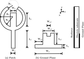
Figure 1 shows the geometry of the antenna, fabricated on a 1.6 mm thick FR4 substrate with permittivity and loss tangent of 4.4 and 0.02, respectively. The proposed antenna is composed of a planar I-shaped monopole and two branch lines of R 1 and R 2 the outer and inner radii, respectively, and then the upper edge of the annular ring is etched by a circle of radius R 3. The two branch lines act as two monopole radiators at the first band and at the same time acts as a cavity resonator fed by the I-shaped monopole that radiates in the upper frequency bands. The two branch lines increase the path over which the surface current flows and that eventually results in lowering the resonant frequency. The electrical length of the two branches is 32.11 mm which is quarter wavelength at the desired narrow band resonance 2.26 GHz. This structure is fed by a 50 Ω microstrip transmission line of width (W f ) 2.2 mm and length (L f ) 12.5 mm at one side of the substrate. On the other side, inverted T-shaped ground plane is printed with a rectangular slot in center T-arm

Fig. 1. Schematic configuration of the proposed fork-shaped antenna.
Figure 2 illustrates the steps involved in the proposed antenna design by using the electromagnetic simulation tool ANSYS “HFSS” [13]. For the case of antenna 1 of circular shape (curve (i)), a single wide band appears over the frequency band, while the resonant mode seems to form at about 4.90 GHz. As for the case of antenna 2 of annular ring shape (curve (ii)), the band is still single. However, the mode is resonating at very low frequency, about 2.8 GHz. Finally, antenna 3 with inclusion of a circular slot is cut at the upper edge and the rectangular strip (curve (iii)) in the design will generates two separate bands first band from 2.24 to 2.68 GHz and second band from 3 to 6 GHz. It provides good performance and covers all the 2.4/5.2/5.8-GHz WLAN and 2.5/3.5/5.5-GHz WiMAX bands. Note that in these cases all the unmentioned dimensions are the same as listed in Table 2.

Fig. 2. Simulated return loss against frequency for circular, annular ring, and the proposed fork-shaped antenna.
Table 2. Design parameters of the proposed antenna shown in Fig. 1.

Based on the optimized parameters given in Table 2, a prototype for the proposed antenna was fabricated and tested. The photograph of the fabricated antenna is shown in Fig. 3. The simulated surface current distribution at different frequencies, 2.5, 3.5, and 5.5 GHz are shown in Figs 3(c)–3(e). It is observed from Fig. 3(c) that the strong surface current flows along the entire patch radiator and feed line. It is observed that the circular arm of fork-shaped radiator generates the lower resonant mode of 2.5 GHz. For the resonance at 3.5 GHz as shown in Fig. 3(d), it is found that the surface current is distributed over the central arm of the fork-shaped radiator and the middle portion of the ground plane. Furthermore, the results in Fig. 3(e) divulge that surface current of the third resonant mode (5.5 GHz) is mainly distributed on the feed line; the bottom part of the circular arm of the fork-shaped radiator; and the entire ground plane. Thus, it can be concluded that mainly the ground plane is accountable for this mode of resonance.

Fig. 3. Fabricated photograph and simulated surface current densities at various sampling frequencies of the proposed fork-shaped antenna.
III. PARAMETRIC STUDY
All the major design parameters are used to find respective influence on the antenna performance. The outer radius R 1, inner radius R 2, radius of the defect to form a fork-shape R 3, length L g1, L g , and width W g of the ground plane are chosen for the parametric study. At a time, the single parameter is used to parametric study, while for other parameters the optimized values, as listed in Table 2, are used.
A) Patch parameters
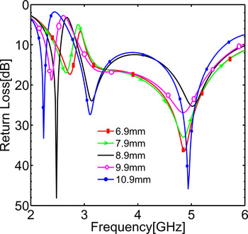
Figure 4 shows the effect of radius R 1 of circular arm of the patch on the return loss of the antenna from 9.5 to 13.5 mm. It is found from Fig. 4 that it mainly affects the first band and the bandwidth of the second band as varied from 9.5 to 13.5 mm. It is also observed that the starting frequency of the second band is moving down as the radius varies up to 11.5 mm and again shifts toward the higher side afterwards. Thus, the optimum value of the radius R 1 of the circular arm of the patch is chosen as 11.5 mm. The effect of inner radius R 2 of the circular arm of the patch on the performance of antenna is depicted in Fig. 5. It is observed that it decides the frequency of resonant mode of the first band. It can be seen that the resonant mode of the first band is shifted toward the lower frequency as varied from 6.9 to 10.9 mm. Thus, the optimum value for the inner radius R 2 of the fork-shaped patch is taken as 8.9 mm to get resonant mode of first band at 2.5 GHz. Figure 6 shows the influence of the radius of the circular defect R 3 over the antenna performance. It is observed that it mainly influences the frequency of the resonant mode of the first band and the starting frequency of the second band as varies from 2 to 6 mm. Therefore, the optimized value for the radius R 3 of the circular defect is chosen as 4 mm.

Fig. 4. Simulated return loss against frequency for the microstrip-fed fork-shaped antenna with various outer radius R 1; other parameters are the same as listed in Table 1.

Fig. 5. Simulated return loss against frequency for the microstrip-fed fork-shaped antenna with various inner radius R 2; other parameters are the same as listed in Table 1.

Fig. 6. Simulated return loss against frequency for the microstrip-fed fork-shaped antenna with various defect radius R 3; other parameters are the same as listed in Table 1.
B) Ground parameters
Figure 7 shows the effect of length L g1 of the ground plane on the performance of the antenna. It is depicted that as the length L g1 is varied from 5 to 9 mm, it mainly influenced the frequency of the resonant mode of the first band and the starting frequency of the second band. Thus, optimum value of L g1 is chosen as 7 mm. The effect of width W g of the ground on the performance of antenna is shown in Fig. 8. It is keenly observed that it also influenced the frequency of the resonant mode of the first band and the starting frequency of the second band. Thus, the optimum value for the width W g of the ground is chosen as 18 mm. In Fig. 9, the effect of ground length L g is shown. It is depicted from the graphs that L g affects the impedance matching in both the bands. Thus, the optimum value of L g is chosen as 2 mm.

Fig. 7. Simulated return loss against frequency for the microstrip-fed fork-shaped antenna with various length L g1; other parameters are the same as listed in Table 1.

Fig. 8. Simulated return loss against frequency for the microstrip-fed fork-shaped antenna with various length W g ; other parameters are the same as listed in Table 1.

Fig. 9. Simulated return loss against frequency for the microstrip-fed fork-shaped antenna with various length L g ; other parameters are the same as listed in Table 1.
IV. EXPERIMENTAL RESULTS AND DISCUSSION
Agilent N5230A vector network analyzer is used to measure the various parameters of the antenna such as impedance bandwidth, return loss, and radiation patterns. The measured and simulated return loss curves of the proposed antenna are shown in Fig. 10. It is observed from Fig. 10 that the simulated and measured results show relatively good agreement. The differences between the measured and simulated results are due to the effect of SMA (SubMiniature version A) connector soldering, substrate losses, and measurement circumstances. The differences may also be due to indeterminate error of the related dielectric constant and loss tangent during simulation. The antenna shows the measured bandwidth of 410 MHz (2.26–2.67) and 3.78 GHz (3.0–6.78 GHz) at lower and upper bands, respectively. It clearly covers both WLAN 2.4 GHz (2.4–2.484 GHz), 5.2/5.8 GHz (5.15–5.35 GHz/5.725–5.825 GHz), and WiMAX 2.5/3.5/5.5 GHz (2500–2690/3400–3690/5250–5850 MHz) bands. It is also observed from Fig. 11 that the radiation efficiency of the antenna is varied from 45 to 90%.

Fig. 10. Simulated and measured return loss of the proposed fork-shaped antenna.

Fig. 11. Efficiency of the proposed fork-shaped antenna.
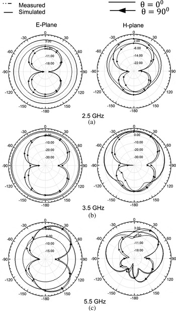
Figures 12(a)–12(c) show the two-dimensional far-field radiation patterns in the H- and E-planes at various sampling frequencies. It is observed that the antenna has nearly good omnidirectional radiation patterns at all operational frequencies in the E-plane (xy-plane). The radiation pattern of a monopole antenna is strongly affected by the finite-sized ground plane. For this conventional monopole antenna, the radiation pattern gets distorted in the H-plane due to radiation of a partial defected ground plane and mismatch of impedance. These patterns are suitable for application in most of the wireless communication equipment operating in WiMAX and WLAN bands, as expected.

Fig. 12. Measured and simulated radiation patterns of the proposed fork-shaped antenna. E-field (xy-plane) and H-field (yz-plane).
V. CONCLUSION
A novel dual-band fork-shaped microstrip antenna is successfully proposed for Bluetooth, WLAN, and WiMAX applications. Measured results show a good agreement with the simulated results. The prototype with compact overall size of 24 mm × 35 mm × 1.6 mm achieves measured bandwidth of 410 MHz (2.26–2.67) and 3.78 GHz (3.0–6.78 GHz) at lower and upper bands, respectively. The proposed antenna is suitable for WLAN 2.4 GHz (2.4–2.484 GHz), 5.2/5.8 GHz (5.15–5.35 GHz/5.725–5.825 GHz), and WiMAX 2.5/3.5/5.5 GHz (2500–2690/3400–3690/5250–5850 MHz) bands applications.
ACKNOWLEDGEMENTS
The authors would like to thank TEQIP(Technical Education Quality Improvement Programme) and college authorities for their continuous support and encouragement during this work.
 Alaknanda Kunwar was born in Chamoli District of Uttarakhand State of India, in 25 May 1986. She received the B. Tech. degree in Electronics and Communication Engineering and received her M. Tech. degree in Digital Signal Processing from G. B. Pant Engineering College, Pauri (Uttarakhand) in 2010 and 2013, respectively. She has published many research papers in reputed journals/conferences such as IEEE, etc. Her main research interests are design and optimization of circularly polarized antennas, RFID, antennas for WLAN/WIMAX applications, etc.
 Anil Kumar Gautam was born in Noida, Uttar Pradesh, India. He received the B.E. degree in Electronics & Communication Engineering from Kumaon Engineering College, Almora, India and the Ph.D. degree in Electronic Engineering from Indian Institute of Technology, Banaras Hindu University, Varanasi, India, in 1999 and 2007, respectively. He joined the Department of Electronics & Communication Engineering, G. B. Pant Engineering College (GBPEC), Pauri, Garhwal, India, in 2000, as an Assistant Professor and he has been an Associate Professor there since 2009. Dr. Gautam is an active member of Board of study (BOS), Academic council, and many other academic committees of GBPEC, Pauri. Dr. Gautam is also member of BOS of HNB Garhwal Central University, India and Uttarakhand Technical University, Dehradun, India. Dr. Gautam is nominated as Nodal Officer, TSP and SCSP Grants by Government of Uttarakhand and executed several projects under these grants. Dr. Gautam has supervised 15 M. Tech. and one Ph.D. thesis, and currently supervising nine Ph.D. theses in the area of Microstrip antenna. Dr. Gautam is the author/co-author of more than 70 research papers published in the refereed international journals and conferences such as IEEE, Microwave, and Optical Technology Letters, Springer, etc. He is the author of the 13 books in the field of Electronics Engineering in the field of Digital Electronics, Antenna and Microwave Engineering. He is a member of IEEE (USA) and many other technical societies. He is also in reviewers panel of IEEE Transaction on Antenna and Propagation, IEEE Antenna and Wave Propagation Letters, IET Microwaves, Antennas & Propagation, Personal and Wireless Communication, Springer, International Journal of Electronics, International Journal of Microwave and Wireless Technologies, International Journal of Antenna and Propagation, etc. His main research interests are in Design and Modeling of Active Microstrip Antenna, Microstrip antennas with Defected Ground Structure, Ultra wide bandwidth antennas, and reconfigurable antennas, reconfiguration antenna array, circular polarized antenna, etc.