


I. INTRODUCTION
At present, a resonant tunneling diode (RTD) is one of the most high-speed semiconductor devices. The detecting properties of RTDs have been demonstrated up to a frequency of 3.9 THz [Reference Scott, Kaminski, Allen, Chow, Lui and Liu1]. An RTD-based microwave oscillator described in [Reference Suzuki, Asada, Teranishi, Sugiyama and Yokoyama2] operates at 1.04 THz and has an output power of 8 µW. In [Reference Smith and Conn3], the authors proposed using an RTD as a nonlinear element in subharmonic mixers. These mixers have been widely used in the intensively developing terahertz frequency range as electromagnetic radiation receivers (detectors) [Reference Rozanov and Rozanov4]. As shown in [Reference Alkeev, Averin, Dorofeev, Gladysheva and Torgashin5], RTD-based mixers have some advantages over the known mixers of this frequency range. The operation principle of RTDs is described in detail in [Reference Sze and Ng Kwok6]. A distinctive feature of an RTD is a delay of electrons in its quantum well (QW) when the current flows through the RTD; therefore, the delay time of electrons in the QW is an important parameter determining the high-frequency properties of RTDs.
The high-frequency properties of semiconductor devices are usually described by small-signal equivalent circuit (EC) models. Figure 1(a) shows an EC of a Schottky diode. This circuit consists of parallel-connected barrier resistance R D, barrier capacitance C D, and a parasitic resistance r S connected in series with this parallel combination. Using this circuit, one can find the cut-off frequency of a Schottky diode in the detector or frequency converter circuits [Reference Gusyatiner and Gorbachev8]:

Fig. 1. (a) EC of a Schottky diode and (b) EC of an RTD with “quantum” inductance [7].
 $$f_{0}=1/2\pi \tau _0\comma \; $$
where τ0 = r SC D.
Sometimes, the EC shown in Fig. 1(a) is used to describe the high-frequency properties of RTDs; nevertheless, a large number of special ECs have been proposed for RTDs (see, for example, [Reference Brown, Parker and Solner7, Reference Feiginov9–Reference Mattia, McWhorter, Aggarwal, Rana, Brown and Maki12]). In [Reference Brown, Parker and Solner7], it was assumed that, under the application of a bias voltage to an RTD, a change in the current flowing through it occurs with some delay; this is equivalent to connecting a so-called “quantum” inductance L Q in series with R D (Fig. 1b). According to [Reference Brown, Parker and Solner7], this inductance is given by
 $$L_Q=\tau _{DL} /G_D\comma \; $$
where τDL is the delay time and G D is the static differential conductance of the RTD. In [Reference Feiginov9], another EC of an RTD with a “quantum” inductance was obtained directly from the equations describing an RTD in the sequential tunneling approximation [Reference Luryi13]. In [Reference Sheard and Toombs10], an EC consisting of two parallel ZC circuits connected in series was suggested in which the impedance Z might depend on frequency. Each ZC circuit simulated one of the barriers of the RTD. This EC was further developed in [Reference Wei, Stapleton and Berolo11, Reference Mattia, McWhorter, Aggarwal, Rana, Brown and Maki12].
Note that it is very convenient to analyze the high-frequency properties of an RTD by the Smith chart. For instance, the impedance curve of the EC shown in Fig. 1(a) is represented by a circular arc on the Smith chart. The impedance curves of the ECs containing a “quantum” inductance are lower than the impedance of the EC shown in Fig. 1(a), while the impedance curves of the EC from [Reference Mattia, McWhorter, Aggarwal, Rana, Brown and Maki12] and other ECs containing additional capacitances are flatter than the arc of a circle on the Smith chart.
The delay time of electrons in the QWs of RTDs was determined by several methods [Reference Scott, Kaminski, Allen, Chow, Lui and Liu1, Reference Tsuchiya, Matsusue and Sakaki14–Reference Feiginov and Chowdhury17]. In [Reference Tsuchiya, Matsusue and Sakaki14], the lifetime of electrons in the RTD QW was determined from the decay time of the photoluminescence intensity. The measured decay time ranged from 6 × 10⁻¹¹ to 8 × 10⁻¹⁰ s for the RTD barrier thickness varying from 2.8 to 6.2 nm (from 10 to 22 monolayers), which is well described by the formula τ = ħ/Γ. Here, Γ is the width of the resonance levels in the QW and ħ is the Planck's constant. Thus, the electron lifetime in the QW is close to the lifetime τD on the resonance level due to the electron tunneling through the emitter and collector barriers. The authors of [Reference Tsuchiya, Matsusue and Sakaki14] also pointed out that the mechanism of electron transport (coherent or sequential) through the RTD cannot be determined from the lifetime measurements. In [Reference Jackson, Johnson, Chow, McGill and Nieh15], the authors determined the electron lifetime in the QW of RTDs from photoluminescence intensity measurements, but with the use of a correlation technique, which enabled them to measure lifetimes as small as 1.2 × 10⁻¹¹ s.
In [Reference Eaves16], the authors used the following formula to determine the delay time of electrons: J = en W/τDC, where J is the current density through the RTD, τDC is the lifetime of electrons in the QW due to tunneling through the collector barrier, and n W is the electron concentration in the QW, which was determined at liquid helium temperature by two methods. In the first method, n W was determined from the period of low-frequency oscillations of the RTD capacitance in a quantizing magnetic field. The second method was based on the determination of the linewidth of the recombination radiation from the RTD QW. Both methods yielded approximately the same results. The delay time of electrons in the QW turned out to be rather large (~6 10−7·s) due to the large thickness of barriers in the RTDs.
In [Reference Scott, Kaminski, Allen, Chow, Lui and Liu1], the authors studied the response of an RTD to the radiation of a free electron laser in the frequency range from 120 GHz to 3.9 THz. The delay time of electrons in the QW was estimated from the frequency dependence of the rectified signal and was found to be 0.24 × 10¹² s.
In [Reference Feiginov and Chowdhury17], the authors studied an RTD based on the InGaAs/AlAs heterosystem with a barrier thickness of 3.5 nm and a QW width of 5.8 nm. They analyzed the frequency dependence of the real and imaginary parts of the RTD impedance in a frequency range of up to 10 GHz and found that the charge relaxation time in the QW varied from 80 to 180 ps depending on the bias voltage, whereas the calculated electron lifetime τD remained approximately constant (120 ps). The authors explained this behavior by the Coulomb interaction between electrons in the RTD.
Note that such a large scatter in the electron lifetime in the QW of various RTDs is natural because the lifetime depends exponentially on the thickness of the RTD barriers [Reference Tager18].
In the present work, we determine the value of the “quantum” inductance by analyzing the shape of the RTD impedance curve on the Smith chart and calculate the delay time of electrons in the QW by formula (2). We derive an expression for the cut-off frequency of an RTD that takes into account both the capacitance of the RTD and the electron delay in the QW. We show that the cut-off frequency essentially depends on electron delay. The analysis of the frequency dependence of RTDs shows that about 10% of the RTDs studied have localized electron states at the heterointerfaces of the active layers. We suggest that these states are due to defects in heterojunctions and arise during the growth of the active layers of RTDs. The recharge of localized electron states, as well as the delay of electrons in the QW, reduces the high-frequency performance of RTDs.
II. EXPERIMENTAL TECHNIQUE AND DATA PROCESSING
We investigated RTDs based on a GaAs/AlAs heterosystem with 1.7-nm-thick AlAs barriers and a 4-nm-wide GaAs QW. The RTDs were designed to be used in millimeter-wave subharmonic mixers. The current–voltage characteristics and other parameters of RTDs are presented in [Reference Alkeev, Averin, Dorofeev, Gladysheva and Torgashin5]. A method for measuring the RTD impedance is described in [Reference Alkeev, Lyubchenko, Velling, Khorenko, Prost and Tegude19]. This method allows one to take into account the impedances of the contact pads and the connecting wires on the RTD chip. We carried out the impedance measurements only in the regions with positive differential conductivity on the I–V curve; in the regions with negative differential conductivity, we could not carry out such measurements because of spurious oscillations.
To choose an EC that best describes the experimental curve of an individual RTD, we used the nonlinear regression method, which allowed us not only to determine the most appropriate EC, but also to find the parameters of this EC. The essence of this method is as follows. At all points f i of the frequency range at which the RTD impedance Z m(f i) is measured, we calculate the impedance Z c(f i) of the assumed EC. Then, we construct a goal function
 $$G=\sum\limits_{i=1}^n {\left\vert {Z_m \lpar f_i \rpar - Z_c \lpar f_i \rpar } \right\vert ^2 }.$$
By varying the parameters of the EC, we find a minimum G min of the function G and the values of the parameters of the EC that minimize the goal function. The EC with the minimum value of G among other ECs is taken as the most appropriate EC for a given RTD. This method also allows us to find the variance (or the RMS error) of the EC parameters [Reference Alkeev, Lyubchenko, Velling, Khorenko, Prost and Tegude19].
III. EXPERIMENTAL RESULTS AND DISCUSSION
The figures below represent the impedance of the active region of an RTD versus frequency on the Smith chart; the impedances of the contact pads and the connecting wires are subtracted from the measured impedance.
Figure 2 shows the experimental impedance of an RTD and the impedance of the EC shown in Fig. 1(a) with optimal values of its parameters. The area of the RTD active region is 10 × 10 µm2, and no bias voltage is applied across the diode. One can see that the calculated curve matches well with the experimental one. The parameters of the optimized EC are as follows: R D = 2.57 kΩ, C D = 0.26 pF, and r S = 0.756 Ω. The cut-off frequency of the RTD, calculated by (1), is about 810 GHz.

Fig. 2. RTD impedance versus frequency in the range from 0.1 to 40 GHz: (1) the experimental RTD impedance when no bias is applied; (2) the impedance of the optimized EC shown in Fig. 1 (a).
A) Delay of electrons in the QW
We investigated the frequency dependence of the impedance of about 30 RTD chips. When no bias is applied, the impedance curves of the majority (~90%) of RTDs well correlated with each other and looked like curve 1 in Fig. 2. We found that these impedance curves are slightly lower than circular arcs on the Smith chart when a bias voltage is applied. Moreover, when the voltage across the RTDs is close to zero or corresponds to the minimum of the valley current on the I–V curve, the impedance curves practically coincide with the arc of a circle. Such an impedance behavior indicates that the effect observed is not related to inaccurate calibration of the measurement equipment. Since such a “sagging” of the impedance curve is typical of the ECs that contain a “quantum” inductance, we suggest that this effect is associated with a delay of electrons in the QW as they pass from the emitter to the collector. To explain the absence of sagging when the voltage across the RTD is close to zero or corresponds to the minimum of the valley current on the I–V curve, we have to assume that the main contribution to electron transfer in these cases is made by non-resonant mechanisms rather than by resonant tunneling.
As an example, Fig. 3 shows the experimental frequency dependence of the RTD impedance (curve 1) at a bias of 0.8 V, which corresponds to the center of the resonant tunneling region on the I–V curve. The area of the active region is 10 × 20 µm2. Curve 2 in Fig. 3 represents the frequency dependence of the impedance of the EC shown in Fig. 1(a) with optimal parameters. One can see that curve 1 is below curve 2. To evaluate the “quantum” inductance, we used the EC shown in Fig. 1(b) and applied the method of nonlinear regression. We found that the “quantum” inductance is 0.09 nH and the delay time of electrons in the QW, calculated by formula (2), is 1.3 ps. We do not show the curve for the EC of Fig. 1(b) with optimal parameters because it nearly coincides with curve 1 in this figure.

Fig. 3. RTD impedance versus frequency in the range 0.1–40 GHz: (1) experimental impedance at a bias of 0.8 V; (2) the impedance of the optimized EC shown in Fig. 1(a).
Based on the EC shown in Fig. 1(b), we derive an expression for the cut-off frequency f C1 of an RTD that takes into account the delay of electrons in the QW. Suppose that an ac voltage U of frequency f is applied to the leads of the EC shown in Fig. 1(b). It can be shown that the voltage U 1 across the resistor R D is
 $$\displaystyle{U \over {1+\lpar r_S /R_D \rpar - \lpar 2\pi f\rpar ^2 \tau _0 \tau _D+j2\pi f\tau _0+j2\pi f\tau _D }}\comma \;$$
where τDL is defined by (2). Note that R D = 1/G R. When the condition R D≫r S is satisfied, we have
 $$\displaystyle{{\left\vert {U_1 } \right\vert } \over {\left\vert U \right\vert }}=\displaystyle{1 \over {\sqrt {1+\lpar 2\pi f\rpar ^4 \lpar \tau _0 \tau _D \rpar ^2+\lpar 2\pi f\rpar ^2 \lpar \tau _0^2+\tau _D^2 \rpar } }}.$$
 Curve 1 in Fig. 4 shows the function |U 1(f)|/|U(f)| calculated by formula (3) with τDL = 0, i.e., for the EC shown in Fig. 1(a). Curve 2 represents the function |U 1(f)|/|U(f)| of the EC with “quantum” inductance shown in Fig. 1(b). The parameters of this EC are the same as those of the EC whose frequency dependence is shown by curve 1 in Fig. 3. One can see that, for the EC with “quantum” inductance, the function |U 1|/|U| decreases with increasing frequency much faster than for the EC in Fig. 1(a). For curve 1, the cut-off frequency (determined from the factor of  $\sqrt 2$ decrease in |U 1|/|U|) is equal to 810 GHz, while the cut-off frequency f C1 for the EC with an inductance is ~125 GHz, which is six and a half times less than the previous one. Thus, taking into account the “quantum” inductance significantly reduces the cut-off frequency of RTDs. Note that f C1 can be found directly from (3). For this purpose, one should equate the radicand (3) to two and solve the quadratic equation for f Reference Suzuki, Asada, Teranishi, Sugiyama and Yokoyama2. However, the expression obtained for f C1 is cumbersome and difficult to analyze.

To assess how the delay time τDL of electrons in the QW depends on barrier thickness, we take into account that, just as in [Reference Tsuchiya, Matsusue and Sakaki14], τDL coincides with the lifetime τDC of electrons in QWs due to tunneling through the collector barrier, and apply the following formula from [Reference Tager18]:
 $$\tau _{DL}=\displaystyle{{2a} \over {v_1 \left\vert T \right\vert ^2 }}.$$
Here, a is the width of the QW, v 1 = (2ɛ1/m*)1/2 is the speed of transverse motion of electrons on the first resonance level with energy ɛ1, m* is the electron effective mass, and |T|Reference Suzuki, Asada, Teranishi, Sugiyama and Yokoyama2 is the transparency of the collector barrier, i.e., the probability of electron tunneling through the barrier. In the case of a rectangular barrier [Reference Tager18], we have
 $$\left\vert T \right\vert ^2=\left[{1+\displaystyle{1 \over 4}\displaystyle{{\sinh ^2 \left\vert \kappa \right\vert b} \over {1+\varepsilon _1 /V\lpar 1 - \varepsilon _1 /V\rpar }}} \right]^{ - 1}\comma \;$$
where b is the barrier thickness, V is the barrier height, and  $\left\vert \kappa \right\vert =\displaystyle{1 \over \hbar }\sqrt {2m \ast \lpar V - \varepsilon _1 \rpar } $. Note that formula (4) is valid in the case of |T|Reference Suzuki, Asada, Teranishi, Sugiyama and Yokoyama2≪1. For our RTDs, V ≈ 1.0 eV, a = 4 nm, and ɛ1 ≈ 0.19 eV. Table 1 shows the calculated transparency |T|Reference Suzuki, Asada, Teranishi, Sugiyama and Yokoyama2, delay time τDL, the RTD cut-off frequency f C1, and the frequency f DL = 1/2πτDL. This frequency coincides with the frequency f C1 when τ0 = 0; i.e., it shows the contribution of the electron delay to the cut-off frequency of RTDs. Calculations were carried out for the barrier thickness of 4, 6, 8, and 10 monolayers.
Table 1. Dependence of high-frequency RTD properties on the barriers thickness.

Table 1 shows that the cut-off frequency f C1 tends to the value 1/2πr SC D = 810 GHz as the barrier thickness decreases. Since r SC D is practically independent of the RTD active area, to increase the cut-off frequency of the RTD, one should reduce the specific contact resistance and the specific capacitance of the RTD. In this relation, RTDs based on the InGaAs/AlAs heterosystem are more advantageous. The specific resistance of non-alloyed ohmic contacts to InGaAs is an order of magnitude lower than the specific ohmic resistance of alloyed ohmic contacts to GaAs [Reference Blank and Goldberg20]. Other advantages of RTDs based on the InGaAs/AlAs heterosystem are the larger barrier height, which increases the temperature stability of these RTDs, and the longer mean-free path of electrons in InGaAs as compared with that in GaAs [Reference Krishnamurthy, Sher and Chen21]. Table 1 also shows that f DL rapidly decreases with increasing thickness of the barriers. Moreover, we can argue that, for a reliable operation of RTD-based mixers at frequencies above 1 THz, the thickness of the diode barriers should not exceed six monolayers.
Note that the greater value of τDL in our RTDs in comparison with the calculated value (0.032 ps) is likely to be attributed to the increased thickness of the RTD barrier layers, which exceeds six monolayers. This follows from the fact that the peak current density in our RTDs is seven times lower than that in the RTDs from [Reference Brown, Goodhue and Sollner22], which have a barrier thickness of six monolayers.
B) Heterointerface defects
About 10% of RTDs investigated in this study had flatter impedance curves than a circular arc. One of these impedance curves (curve 1) is shown in Fig. 5.
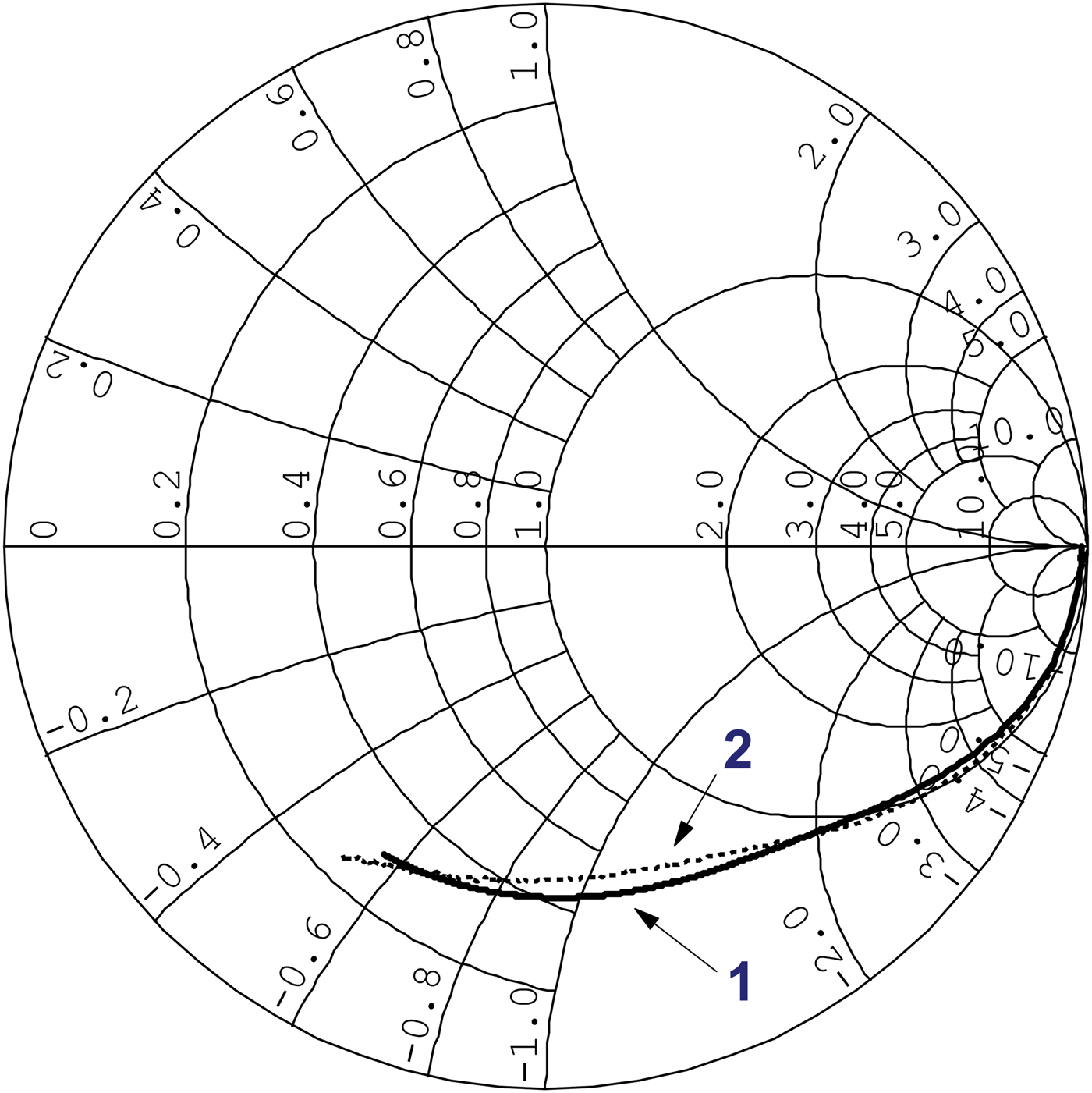
Fig. 5. (1) The experimental impedance of an RTD and (2) the impedance of the optimized EC shown in Fig. 7(a), in the frequency range 0.1–40 GHz.
The flatter shape of the curves was also observed in the RTD samples from Duisburg University (Germany) [Reference Alkeev23]. InAlAs RTD barriers were 5 nm thick, the width of the InGaAs QW was also 5 nm, and the area of the active region was 50 µm2. Figure 6 shows a part of the Smith chart. Curve 1 represents the experimental RTD impedance at a bias of 0.3 V, and curve 2 represents the impedance of the EC of Fig. 1(a) with optimal parameters (i.e., for G = G min). We can see that curve 1 is flatter than curve 2.

It turned out that the impedance curve that is flatter than a circular arc is well described by the EC proposed in [Reference Jo, Li, Chen and Wang24] and shown in Fig. 7(a). Curve 3 in Fig. 6 shows the impedance of the EC shown in Fig. 7(a) for G = G min. We can see that curve 3 fits the experimental curve 1 much better than curve 2. Quantitatively, G min for the EC shown in Fig. 7(a) is more than an order of magnitude smaller than G min for the EC shown in Fig. 1(a).

Fig. 7. (a) EC of an RTD from [24] and (b) EC of a MOS structure from [6].
The C WR W circuit in Fig. 7(a) is similar to an analogous circuit of a MOS structure shown in Fig. 7(b) [Reference Sze and Ng Kwok6], which describes the recharge of the surface states of the structure by a high-frequency electric field. Here, C i and C D are the capacitances of the insulator and the semiconductor depletion layer, respectively. The value C SR S determines the relaxation time of the surface states. By analogy with the circuit shown in Fig. 7(b), we assume that the C WR W circuit in Fig. 7(a) describes the recharge of localized electron states at the RTD heterointerfaces. For the RTDs from Duisburg University, the values of C W and R W at the minimum of the goal function were equal to 0.042 pF and 350 Ω, respectively, and the recharge time of surface states was found to be 14.7 ps.
For the RTD whose impedance is shown by curve 1 in Fig. 5, we determined the parameters of the EC shown in Fig. 7(a) by the nonlinear regression method. The impedance of this EC for G = G min is shown by curve 2 in Fig. 5. The values of C W, R W, and r S were equal to 0.12 pF, 217 Ω, and 10.9 Ω, respectively, and the recharge time of the surface states was found to be 26 ps.
Thus, we can assume that the flatter shape of the impedance curve for 10% of RTDs is associated with damaging the heterointerface structure during the growth of the active layers of RTDs and the appearance of localized electron states at the heterointerfaces. These states, similar to the surface states on the SiO2−Si interface, are recharged in an ac electric field.
To assess the influence of defects at the heterointerfaces on the high-frequency properties of RTDs, we determine the cut-off frequency f C2 for the circuit shown in Fig. 7(a). We will do this in the same way as the formula for the cut-off frequency f C0 was obtained in [Reference Gusyatiner and Gorbachev8].
Suppose that a high-frequency voltage U is applied to the leads of the EC in Fig. 7(a). Let us calculate the voltage U 1 across the resistor R D: U 1 = UZ 2/(r S + Z 2), where Z 2 is the impedance of the circuit consisting of parallel-connected R D and C D and the R WC W circuit connected in series with them. The analysis has shown that if R D, R W≫r S, then |U 1|/|U| weakly depends on C W, and its frequency dependence is the same as that of the EC shown in Fig. 1(a):  $\left\vert {U_1 } \right\vert /\left\vert U \right\vert =\sqrt {1+\lpar 2\pi \rpar ^2 f^2 \tau _0 } $; therefore, f C2 = f C0.
The fact that the R WC W circuit produces no effect on the f C2 of these RTDs can be explained as follows. The recharge time τW of the circuit R WC W is rather large due to the large value of R W; therefore, the capacitance C W cannot be recharged in a high-frequency electric field. As τW decreases when C W tends to zero, the circuit R WC W ceases to influence f C2 due to the smallness of C W. Thus, the cut-off frequency of the RTDs with flat frequency dependence of the impedance does not depend on the recharge time of localized electron states at the RTD heterointerfaces. However, one should pay attention to the following two features of these RTDs: a large value of R D (Fig. 5) and an enhanced parasitic series resistance r S of up to ~10–20 Ω, which, according to formula (1), leads to a decrease in the cut-off frequency.
Note that the method based on the analysis of the frequency dependence of the impedance is highly informative. For instance, the shape of the I–V curve of the RTDs whose impedance versus frequency is close to an arc of a circle on the Smith chart nearly coincides with the shape of the I–V curve of the RTDs whose impedance exhibits flatter frequency dependence than the arc of a circle; i.e., the shape of the I − V curves does not allow one to find out if there are localized electron states at the heterointerfaces of RTDs.
IV. CONCLUSIONS
We have investigated the frequency dependence of the impedance of RTDs based on the GaAs/AlAs heterosystem with 1.7 nm barriers and 4 nm QWs that are intended for use in millimeter-wave subharmonic mixers operating in the range from 0.1 to 40 GHz. The measured results have been compared with the frequency dependence of the impedance of various ECs of RTDs on the Smith chart. The analysis has shown that, at zero dc bias, the high-frequency properties of the majority (~90%) of RTDs are well described by an EC consisting of parallel-connected resistance and capacitance and an additional resistance connected in series with this parallel circuit. The frequency dependence of the impedance in this case is represented by an arc of a circle on the Smith chart. When a bias voltage is applied to the diodes, the curves of their impedances lie below the arc of a circle on the Smith chart. Such a “sagging” of curves was observed only in the sections of the I–V curve where the resonant tunneling of electrons occurs. This effect is well described by the EC containing a “quantum” inductance L Q. The value of L Q has allowed us to calculate the delay time of electrons in the QWs of RTDs.
We have obtained an expression for estimating the RTD cut-off frequency that takes into account the delay of electrons in the QW. Our evaluation has shown that the cut-off frequency of our RTDs is 125 GHz, which is six and a half times lower than the cut-off frequency of RTDs when the delay of electrons in the QW is neglected.
We have calculated the electron delay time in the QW as a function of the RTD barrier thickness. These calculations show that the RTD cut-off frequency is greater than 1 THz provided that the barrier thickness of the diodes does not exceed six monolayers.
To describe the high-frequency properties of the remaining ~10% of RTDs, it is necessary to use an EC that takes into account the recharge of localized electron states at the RTD heterointerfaces. These states can be attributed to the destruction of the heterojunction structure during the growth of the active layers of RTDs and degrade the performance of RTDs by increasing the parasitic series resistance.
Note that the method based on the analysis of the frequency dependence of RTD impedance is highly informative. For instance, our investigations have shown that the I–V curves of RTDs with localized electron states on the heterointerfaces nearly coincide with the I–V curves of ordinary RTDs.


