I. INTRODUCTION
Due to the down-scaling and resulting high transit frequencies, CMOS is becoming a realistic alternative to III–V technologies for microwave applications, also at higher frequencies than today's commercial applications in the lower GHz-region. Several successful design examples well up into the V-band have been published, e.g. [Reference Ferndahl, Motlagh, Masud, Angelov, Vickes and Zirath1–Reference Heydari, Bohsali, Adabi and Niknejad4]. Surprisingly, little has however been reported regarding CMOS power amplifiers at frequencies above 10 GHz. The results by Ferndahl et al. [Reference Ferndahl, Johansson and Zirath5] represent highest power, with 18.3-dBm output at 20 GHz, whereas LaRocca and Chang [Reference LaRocca and Chang6] with 12.2 dBm at 60 GHz represent highest power combined with high frequency. Investigations on device level have also been carried out by Scholvin et al. [Reference Scholvin, Greenberg and del Alamo7] and Ferndahl et al. [Reference Ferndahl, Vickes, Zirath, Angelov, Ingvarson and Litwin8, Reference Ferndahl, Nemati, Parvais, Zirath and Decoutere9].
While the short channel lengths have enabled excellent small-signal high-frequency performance, it has also led to lower breakdown voltages and thus a smaller tolerable RF voltage swing. As a result the maximum output power is reduced and the design of CMOS power amplifiers becomes challenging. Hence, there is a need to study CMOS power amplifiers above 10 GHz to understand how, e.g., higher output power can be achieved.
This paper reports a study of power amplification at 20 GHz in 130-nm CMOS technology. The presented findings are based on both large signal transistor measurements and five different power amplifier designs, exploring different transistor types, single transistor versus cascode, combining power amplifiers as well as the effect of total transistor gate width.
Furthermore, the modeling of the transistors, using RF extension to the intrinsic model, is presented as well as the modeling of the passive components in the matching network.
The paper is organized as follows. Section II explains the modeling of the transistors and passive components. In Section III the result of small and large signal measurements of several different transistor layouts and types are presented. The circuit design is covered in Section IV and results in Section V. Comparisons and conclusions are made in Sections VI and VII, respectively.
II. MODELING
The available transistor model for the used process is based on the BSIM4 model, with some extensions of library cells to handle the layout parasitics up to the polysilicon/metal 1 layers. To include the effects of the metal interconnects up to the top metal layer, series resistances and inductances were added to all three terminals (gate, drain, source), see Fig. 1(a). The bulk terminal was connected directly to the source terminal.

Fig. 1. (a) Intrinsic BSIM4 model with RF extension. (b) Layout of transistor test structure with package model of pad capacitances and access lines overlayed used in the de-embedding.
Before the extraction of the parameter values for the RF extension the measured S-parameter data was de-embedded to remove the influence of pad capacitance and access lines in the test structure, see Fig. 1(b). The pads and access lines to the device are thus not part of the RF extension. A statistical equivalent-circuit-based de-embedding procedure was used [Reference Ferndahl, Fager, Andersson, Linnér, Vickes and Zirath10] with the package model shown in Fig. 1(b).
The parameter values of the RF extension, describing the parasitics upto the top metal layer, there the transmission lines are connected, to the polysilicon/metal 1 layer, were then found through a multi-bias optimization using measured extrinsic (de-embedded) data and simulated intrinsic data.
Standard transmission lines models were used with parameters based on process information such as substrate thickness and conductivity. These models were also validated using 2.5D EM simulations and found sufficiently accurate, at these frequencies. The models for the input and output pad capacitance were taken from the de-embedding data, using an RC series network, i.e. C p1 and R p1 in Fig. 1(b).
III. EVALUATION OF 130-NM CMOS FOR 20 GHZ POWER AMPLIFIERS
To evaluate 130-nm CMOS as a technology for power amplification around 20 GHz, several devices were fabricated and measured to evaluate their performances. The measurements were carried out in two steps. First bias dependent small signal measurements were performed, using a network analyzer up to 50 GHz to find the available gain at 20 GHz and also extract the parameter values for the RF extension mentioned in Section II. The most promising devices were then measured in a large signal setup to find their maximum output power and their corresponding optimal input and output impedance levels using load and source pull with impedance tuners.
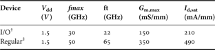
At lower frequencies it is quite common to use I/O transistors with thicker oxide and longer gate lengths as they allow a higher drain voltage supply and therefore can deliver more output power at a higher impedance level. Therefore, I/O transistors were measured and compared to regular transistors with minimum gate length having nominal oxide thickness. The gain of the I/O transistors were, however, too low at these frequencies, i.e. above 10 GHz, to be usable in a power amplifier design, and regular transistors had to be used, see Table 1.
Table 1. Comparison between different device options in a 130-NM RF-CMOS process*.

* Transistor gate width 10 µm ×100 fingers (not optimized for maximum gain).
†Thick gate oxide and larger gate length.
‡Thin gate oxide and minimum gate length.
The regular transistor, with minimum gate length, was designed with different layouts, having 1-mm total gate width and varying unit gate finger width, from 5 µm and up. This in order to find an optimum in terms of both gain, output power, and reliability. The layout of large transistor cells for power amplification at high frequencies, about a fifth of f T, is problematic from two aspects. First, the gate finger width should be kept short enough to have sufficient gain, since the high gate resistance from a wide gate finger transistor will deteriorate the high-frequency performance. The second issue is how to layout a multi-finger transistor to avoid problems with electromigration and reliability due to the large drain/source currents, this while keeping the parasitic capacitances and resistances as low as possible. For example the source return path, drawn above the drain and gate connection, was too narrow in the 5 µm × 200 finger transistor layout with almost immediate degradation during large signal measurements. A unit gate finger width of 10 µm gave satisfactory performance in terms of both gain and metal current density-related reliability. The resulting measured maximum output power, gain, and power-added efficiency (PAE) for the 100 fingers × 10 µm device are shown in Fig. 2. The maximum achieved output power density at 3-dB compression was 148 mW/mm with a maximum PAE of 20%. To the authors' knowledge this is the highest reported output power density for CMOS at these frequencies. The gain of the 1-mm device was, however, too low (5 dB) and smaller transistor sizes (200 and 500 µm total gate width) were chosen for the power amplifier designs. Two sizes were chosen to be able to obtain insight on the effect of device size in the amplifier design. The transistors were also put in a cascode configuration. As the supply voltage in the cascode cell is partitioned between the input and the output/common gate transistor, see Section VI, a higher supply voltage may be used which will increase the output power.

Fig. 2. Measured transducer gain, output power and PAE from load pull characterization of a 1-mm gate width 130 nm CMOS at 23 GHz. Source and load impedance were optimized for maximum output power (ZS = 9–0.13, ZL = 9.2–0.16).
IV. CIRCUIT DESIGN
Five different power amplifiers were designed and characterized: single transistor power amplifiers, cascode power amplifiers, both with 200 and 500 µm transistors, and a power amplifier with two 200-µm cascode power amplifiers, which were combined on-chip using Wilkinson combiners. Figure 3 gives an overview of the schematics.

Fig. 3. Schematic of (a) the single transistor power amplifiers, (b) the cascode power amplifiers, and (c) two combined cascode power amplifiers.
All power amplifiers were single stage. Additional gain can be added by using one or several driver stages in front of the power amplifiers, but will not affect the maximum output power, which was of main interest in this study. Microstrip transmission lines were used as matching elements with the signal line in the top metal layer and ground plane in the bottom metal layer. Distributed components were chosen over lumped due to ease of modeling the transmission lines and lack of accurate inductance models in the design environment. The drawback of the distributed approach is a larger chip area, although the present designs could be shrunk considerably with more aggressive meandering. All transmission lines were designed to have a 50-Ω characteristic impedance, except for the shorted stubs to the drain, which were made 20 µm wide, corresponding to an impedance level of 27 Ω. The wider drain line helps to accommodate the large drain current, so that problems with electromigration and/or Joule heating are avoided. The lengths of the lines, and stubs were appropriately chosen for best performance in terms of matching, gain, and output power.
The power amplifiers were fabricated in a 130-nm RF CMOS process with four Cu layers, two thick top Al metal layers, and MIM capacitors. The designs were made using Agilent's ADS simulator and Cadence layout environment. Chip photos of the power amplifiers can be found in Fig. 4.

Fig. 4. Chip photo of the five different power amplifiers.
V. RESULTS
The power amplifiers were measured on wafer with 1.5-V drain bias for the single transistor power amplifiers and 3.0-V drain and cascode bias for the cascode power amplifiers. The gain versus output power at 20 GHz for all five power amplifiers are presented in Fig. 5.

Fig. 5. Transducer gain versus output power for the single transistor 200-µm power amplifier (a), the 200-µm cascode power amplifier (b), the two combined 200-µm cascode power amplifiers (c), the single transistor 500-µm power amplifier (d), and the 500-µm cascode power amplifier (e). All at 20 GHz.
A comparison with simulated and measured S-parameter data of the combined 200-µm cascode amplifiers shows good agreement, see Fig. 6, although a slight frequency shift toward lower frequencies is observed. The transducer gain and PAE of both the combined 200-µm cascode power amplifier and the 200-µm cascode power amplifier show very good agreement between simulation and measurement, see Figs 7 and 8.

Fig. 6. Measured (crosses) and simulated (solid lines) S-parameters of the combined 200-µm cascode power amplifier.

Fig. 7. Measured and simulated transducer gain and PAE of the 200-µm cascode power amplifier.

Fig. 8. Measured and simulated transducer gain and PAE of the combined 200-µm cascode power amplifier.
The agreement between both small and large signal simulations and measurements shows that the used models are valid both for the transistors and passive matching networks, including the Wilkinson combiner. Furthermore, in Fig. 8 the simulated transducer gain without the RF-extension of the transistor model is shown. As can be seen from the figure the simulation without the RF extensions overestimates the gain with almost 2 dB, corroborating the need of the RF extension for accurate simulations.
A summary of these and previously published power amplifiers is made in Table 2.
Table 2. Summary of results and comparison of 10–40 GHz CMOS power amplifiers

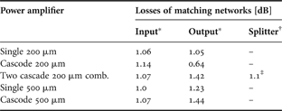
Even though a thick top metal layer is used for the transmission lines in the matching network, the Q-value is still quite limited due to a lossy dielectric, the SiO2, and resistive losses in the metal. The partitioning of the losses between the input and output matching network as well as the power splitter/combiner were simulated and is presented in Table 3. The input and output matching networks contribute together with about 2 dB to the loss. The combiner adds another 1.1 dB in loss, but as the combination of two power amplifiers will add 3 dBm it is still beneficial to use a power combining scheme to increase the output power.
Table 3. Loss partitioning in the different power amplifiers.

*Including input or output MIM capacitors and bias network.
†Combiner at output is the same.
‡Only the loss, i.e. excluding the 3 dB due to the splitting.
VI. DISCUSSION ON THE LIMITS FOR 20 GHZ POWER AMPLIFIERS
From the data in Table 2 it is seen that a cascode configuration is preferred, both from a gain and output power perspective. The output power is higher for the cascode power amplifiers as a higher supply voltage can be applied. This is possible since the drain–source voltage is partitioned between the input and the cascode transistor, as can be seen from Fig. 9, which shows the simulated drain–source voltage waveforms in the 500-µm power amplifier having a 3-V supply.

Fig. 9. Simulated drain and drain–source voltage waveforms for the 500-µm power amplifier with 3-V supply voltage, at 20 GHz.
From Fig. 10(b) it can be seen that the peak voltages exceed the maximum permitted DC supply voltage of the technology, in this case 1.5 V. There are indications, e.g. [Reference Ferndahl, Vickes, Zirath, Angelov, Ingvarson and Litwin8, Reference Ferndahl, Nemati, Parvais, Zirath and Decoutere9, Reference Sasse, Kuper and Schmitz16], that the peak-to-peak can exceed the DC reliability limits; however, more research on the topic is necessary to fully understand these effects. From short-term measurements, i.e. up to 1 h, of the power amplifiers no degradation was seen for any of the presented power amplifiers, even when overdriven with a large input signal, up to 25 dBm during shorter intervals.

Fig. 10. (a) Simulated and measured gain and output power versus supply voltage of the 500-µm cascode power amplifier. (b) Simulated peak-to-peak voltage between source and drain for the common-source and common-gate transistor of the cascode cell. Both at 20 GHz.
The effect on peak-to-peak voltage, gain, and output power versus supply voltage was also studied for the 500 µm cascode power amplifier, see Fig. 10(a). The output power drops slowly with decreased supply voltage to a level around 2 V then the roll off is more pronounced. The gain is, however, unaffected, as expected. The peak-to-peak values follow the output power with a faster roll off, versus lower supply voltage, for the drain–source voltage of the cascode transistor, see Fig. 10(b).
The output power of these and previously published power amplifiers [Reference LaRocca and Chang6, Reference Vasylyev, Weger, Bakalski and Simbuerger11–Reference Komijani, Natarajan and Hajimiri13, Reference Vasylyev, Weger and Simburger17–Reference Yao, Gordon, Yau, Yang and Voinigescu25] are marked versus frequency in Fig. 11. The saturated output power is presented but it is important to realize that the 1 dB compression point in some cases is significantly lower, some examples can be seen in Table 2.

Fig. 11. Output power versus frequency for published power amplifiers in CMOS between 10 and 70 GHz. This paper: (a)–(e).
VII. CONCLUSIONS
Using both device level measurements and a set of different designs, the limits and tradeoffs for power amplifier design in 130-nm CMOS at 20 GHz have been investigated.
Transistor size and configuration as well as the combining of two power amplifiers using Wilkinson splitter/combiners were studied. A maximum output power of 63 mW at 20 GHz for two on-wafer combined cascode power amplifiers and 148 mW/mm from load pull characterization of a single transistor were achieved. Both these values are, to the authors' knowledge, the highest reported above 10 GHz for CMOS. Furthermore, transistor modeling and the layout of transistors for power amplifiers were discussed.
From the results presented in this paper it is concluded that the maximum output power for 130 nm CMOS power amplifier at 20 GHz is between 100 and 200 mW, probably closer to 200 mW. If two of the 500 µm power amplifier presented in this paper were combined on-wafer it would be possible to achieve 100 mW in output power. Combining up to four amplifiers using five-port splitters/combiners is feasible and would result in an output power close to 200 mW.
ACKNOWLEDGEMENT
This work was supported by VINNOVA, Sweden through the European MEDEA+ project HiMission.
 Mattias Ferndahl received an M.Sc. degree in Physics Engineering from Chalmers University of Technology, Göteborg, Sweden, where he is currently employed as a Ph.D. student at the department of Microtechnology and Nanoscience, Microwave Electronics Lab. His research interest is mainly microwave and millimeter wave circuit design and transistor modeling, including characterization methods. He is a author/co-author of more than 30 refereed journal/conference papers, and holds one patent.
 Ted Johansson received an M.Sc. degree in Applied Physics and Electrical Engineering in 1985, and Dr. Tech. and Ph.D. degrees in Electronic Devices from Linköping University, Sweden, in 1993 and 1998, respectively. From 1985 to 1989, he was with the Swedish Institute of Microwave Technology, Stockholm, conducting research in the area of MOS process technology. He joined Ericsson Components AB in 1989 and was heavily involved in the development of RF power transistors for cellular base stations for almost 10 years. His interest then shifted into RFIC technologies, mainly SiGe bipolar and BiCMOS, and integrated power amplifiers for wireless handsets. After the acquisition of Ericsson Microelectronics AB by Infineon Technologies in 2002, he divided his attention between research on SOI for BiCMOS, technology strategy for future RFIC processes (BiCMOS and CMOS), and competitor technology analysis. In 2005, the focus was switched again to power amplifiers for wireless applications, mainly for cordless phones, and the integration of CMOS power amplifiers for SoC solutions. From 2008, he is with Huawei Technologies Sweden AB, specializing in PA design and R&D for wireless terminals. He has published more than 50 journal and conference papers, and holds 35 patents.
 Herbert Zirath received his M.Sc. and Ph.D. degrees from Chalmers University, Göteborg, Sweden, in 1980 and 1986, respectively. He is since 1996 a Professor in High Speed Electronics at the Department of Microtechnology and Nanoscience, MC2, at Chalmers University. He became the head of the Microwave Electronics Laboratory during 2001. At present he is leading a group of approximately 35 researchers in the area of high-frequency semiconductor devices and circuits. His main research interests include foundry-related MMIC designs for millimeter wave applications based on both III–V and silicon devices, SiC and GaN-based transistors and circuits for high power applications, device modeling including noise and large-signal models for FET and bipolar devices, and InP-HEMT devices and circuits. He is a working part-time at Ericsson AB as a microwave circuit expert. He is author/co-author of more than 300 refereed journal/conference papers, and holds four patents.